
Abstract
An ultra-thin (5 nm-thick), unpassivated zinc tin oxide (ZTO) thin-film transistor TFT, fabricated with solution process, exhibits a good field-effect mobility (13 ∼ 14 cm2/Vs), small subthreshold swing (∼0.30 V/dec.) and high on/off current ratio (∼108). The field-effect mobility can be further enhanced by increasing the ZTO thickness to 12 nm and 22 nm. Furthermore, ID-VG characteristics of the 5 nm-thick ZTO TFT remain unaffected, regardless of working in air (60% relative humidity), vacuum or dry O2 atmosphere. The dissimilar TFT characteristics are discussed in terms of oxygen deficiency content, as well as the Fermi level position (EF to EC) for ZTO of various thicknesses to explain the moisture immunity of the 5 nm-thick solution-processed ZTO TFT.

This is an open access article distributed under the terms of the Creative Commons Attribution 4.0 License (CC BY, http://creativecommons.org/licenses/by/4.0/), which permits unrestricted reuse of the work in any medium, provided the original work is properly cited.
Zinc oxide-based thin film transistors (TFTs) have been applied in a wide range of electronic circuits, such as flat-panel displays, light emitting diodes and charge trapping non-volatile memory.1–2 Among them, zinc tin oxide (ZTO) TFT that is indium- and gallium-free has gained an advantage because of the low-cost competition.3–5 In addition, the solution process has attracted much attention for TFT fabrication since it enables process simplification and high throughput even for large-area displays, thereby providing a reduction in manufacturing costs for flat-panel displays.6 Furthermore, the stability and reliability of TFTs has been intensively studied in recent years, which are one of the most important issues for their practical application.7–8 Thus, our previous study had investigated transistor characteristics and bias stability with and without light illumination for solution processed ultra-thin ZTO TFTs without passivation.9 However, for unpassivated devices, the back surface of metal oxides are sensitive to the ambiance (oxygen, water and/or dipole molecules), which may be the dominant factors affecting the threshold voltage (Vth).10–12 The comparison of back and front channel conduction in ZnO-based TFT, using ionic liquid and SiO2 dielectrics, respectively, has also been reported.13 On the other hand, the effect of active layer thickness on the electrical performance of oxide TFTs has been investigated for oxide TFTs,14–16 including solution processed ZTO.17 However, not much attention has been paid on the characteristics of TFTs with ultra-thin active oxide films (less than 10 nm). In addition, oxygen vacancy content in ZTO may be thickness dependent and will influence the ambient effect as well. In this work, we report the ZTO thickness dependence of oxygen deficiency content and its impact on electrical characteristics with different ambiances for solution processed ZTO TFTs. The relationship between oxygen deficiency content and adsorption of water molecules by comparing the TFT performance in air (relative humidity of 60%), vacuum (3 × 10⁻⁵ torr) and dry O2 (760 torr) atmosphere for varying ZTO thickness are investigated in detail.
Experimental
The bottom-gate, top contact ZTO TFTs were fabricated on p-type Si (the gate electrode) substrates. A solution process was used to fabricate the ZTO semiconductor films. Zinc nitrate hexahydrate (Zn(NO3)2·6H2O) and tin chloride dihydrate (SnCl2·2H2O) were used as precursors for preparing the molar ratio of Zn:Sn = 1:1. The ZTO solution was then mixed with ethylene glycol monomethyl ether (without adding any chelating agent), and magnetically stirred for 20 hours to ensure chemical homogeneity. In order to obtain ultra-thin ZTO films, we diluted the metallic concentration of ZTO solution to only 0.1 M and coated the film with high spin speed of 4000 rpm for 60 s. Subsequently, the ZTO precursor solution was spin-coated onto a p-type Si wafer with 110 nm thick SiO2 and subsequently heated at 500 °C on a hot-plate in air for 2 min. The process was repeated for 1, 3 and 5 times, controlling the total thickness at around 5, 12 and 22 nm, respectively. The spin-coated ZTO layer was rapidly annealed at 500 °C for 1 h under an air atmosphere. The Si substrate, ZTO and SiO2 function as the gate electrode, active layer and gate dielectric, respectively. Afterwards, the Al source and drain electrodes (300 nm thick) were evaporated by E-beam evaporation through a shadow mask to define the TFT channel width (2000 μm) and length (100 μm). The thickness was characterized using a transmission electron microscope (TEM, JEOL JEM-2100F). The impact on the chemical bonding states with different thickness of ZTO films were studied using X-ray photoelectron spectroscopy (XPS, JEOL JAMP-9500F) and correlated directly with observed changes in Fermi level position were measured by ultraviolet photoelectron spectroscopy (UPS, Thermo VG-Scientific Sigma-Probe). Finally, all of the electrical characteristics of the ZTO TFTs were measured under air with relative humidity of 60%, vacuum (3 × 10⁻⁵ torr) and dry O2 (760 torr) atmosphere in a chamber system and probe station using an Agilent 4156 C semiconductor parameter analyzer.
Results and Discussion
Figures 1a, 1b and 1c show the cross-sectional TEM images of ZTO films with multiple spin-coatings. Note that the TEM specimens of ZTO films were prepared by depositing ZTO onto a thin 5 nm SiO2 grown-on Si substrate and covered with an Al protection layer. No distinct layer-to-layer interface can be found in the ZTO films spin-coated for three times (Fig. 1b) and five times (Fig. 1c). Therefore, the microstructure of multiple spin-coated ZTO films is homogeneous in depth and the thicknesses of ZTO, as measured from the images, are about 5, 12 and 22 nm, respectively. A thin interfacial layer is present between ZTO and Al, which is AlOx as characterized by energy dispersive spectrometry (EDS) and is likely formed after the Al deposition process.
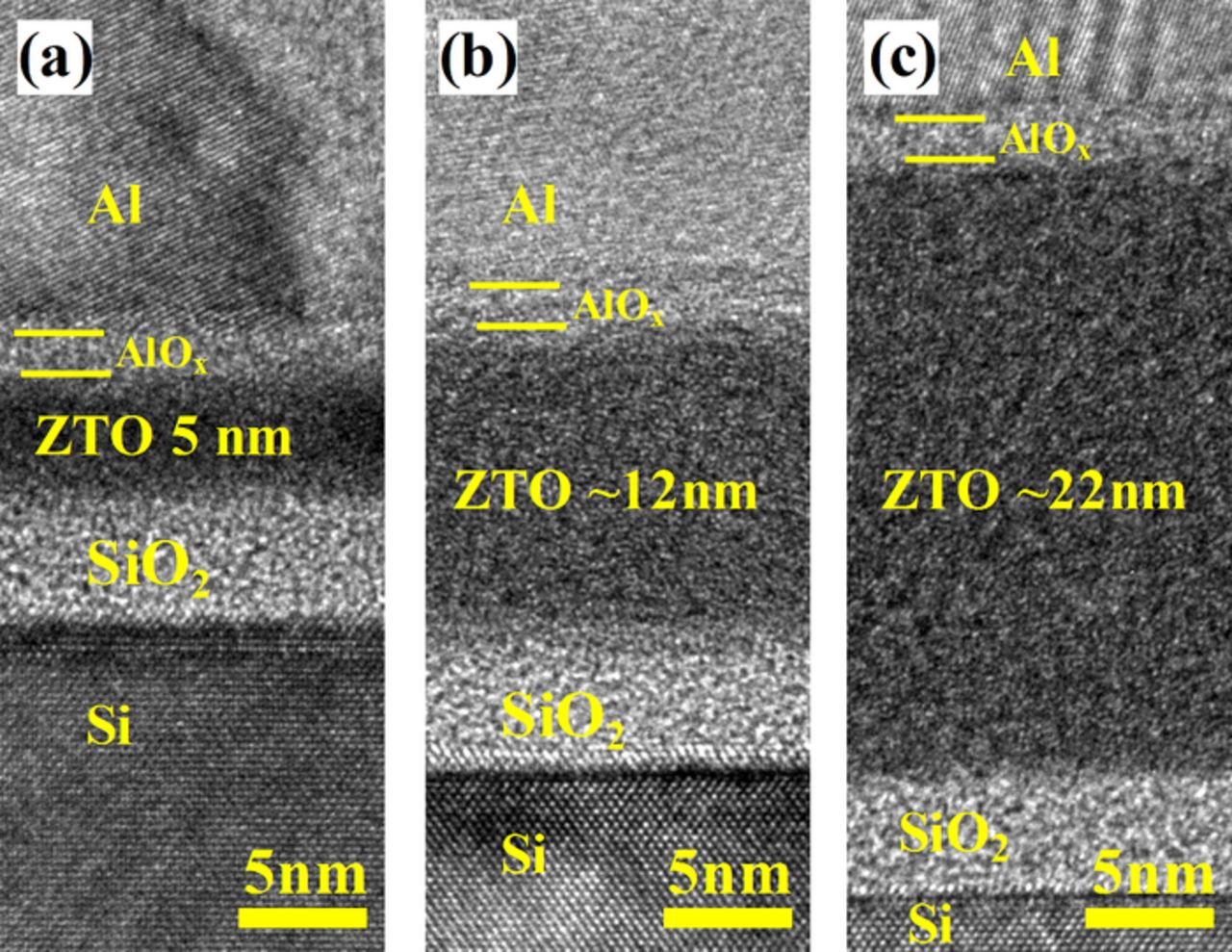
Figure 1. Cross-sectional TEM images of multiple spin-coated ZTO films with thickness of (a) 5 nm, (b) 12 nm and (c) 22 nm on SiO2 (5 nm)/p-Si substrate.
To evaluate the effect of thickness and ambiances on electrical performance of ZTO TFTs, Figures 2a, 2b and 2c show the ID-VG curves of ZTO TFTs with ZTO thicknesses of 5, 12 and 22 nm, measured under air, vacuum (3 × 10⁻⁵ torr) and dry O2 (760 torr), respectively. The inset show the leakage current (IG) of three ZTO TFTs with different atmospheres. As previously reported, adsorption of H2O molecules in the ambient (relative humidity larger than 40%) causes significant negative threshold voltage (Vth) shifts in unpassivated oxide-based TFTs.18–19 In this study, the experiment was performed in air with relative humidity of 60%. To discuss more insight into the interaction of O2 molecules and avoid H2O adsorption on ZTO films at the initial state of TFT devices, all devices were put into a vacuum chamber (3 × 10⁻⁵ torr) for 6 hour and then dry O2 gas was vented into the chamber until the chamber pressure reached 760 torr. As a result, the IG of all of ZTO TFTs shows no difference at various ambiances. However, IG value of all TFT devices is noticeable in the turn-on region (about 0.04ID∼0.05ID) because of using the non-pattern Si-gate substrate.20 The slope of the linear fitting (ID)1/2-VG curve is used to estimate the saturation field-effect mobility (μFE), while the intercept of the extrapolated line with the X-axis defines the threshold voltage (Vth). The subthreshold swing (S.S.) values are extracted from the slope of the log(ID)-VG curve. Off current (ID-off) and on current (ID-on) are defined as the minimum and maximum drain current, respectively, in each ID-VG curve. The electrical parameters of all TFTs are summarized in Table I. First of all, the solution processed ZTO exhibits good μFE, which is about 13∼14 cm2/Vs for 5 nm-thick ZTO and μFE reaches 26∼29 cm2/Vs for 22 nm-thick ZTO. However, expanding ZTO thickness may also be detrimental to Vth, S.S. value, and on/off current ratio, as apparently seen in Fig. 2 and Table I. Additionally, the transistor characteristics of 5 nm-thick ZTO TFT are insensitive to the ambiances but the Vth, S.S. value and ID-off of 12 nm- and 22 nm-thick ZTO TFTs change significant when measured in air and vacuum. Meanwhile, there is no apparent change of the transfer characteristic curves measured either under vacuum or in dry O2 ambiance. All three devices are not passivated on the back surface. It is intriguing to know why the ambiance (air vs. vacuum or dry O2) does not have any impact on the ID-VG characteristics of the 5 nm-thick ZTO TFT.
Table I. Comparison of the electrical characteristics measured in air ambiance vacuum, and dry O2 including μFE, Vth, S.S., ID-on, ID-off and ID-on/ID-off ratio for solution-processed ZTO TFTs with ZTO thickness of 5, 12 and 22 nm.
| μFE (cm2/Vs) | Vth (V) | S.S. (V/dec.) | ID-on (A) | ID-off (A) | Ion/Ioff ratio | |
|---|---|---|---|---|---|---|
| Air ambiance | ||||||
| ZTO (5 nm) | 13.8 | 6.77 | 0.32 | 4.80 × 10⁻³ | 1.79 × 10⁻¹¹ | 2.68 × 10⁸ |
| ZTO (12 nm) | 21.7 | 0.92 | 0.97 | 1.00 × 10⁻² | 5.08 × 10⁻⁸ | 1.97 × 10⁵ |
| ZTO (22 nm) | 26.1 | −8.05 | 2.22 | 1.00 × 10⁻² | 4.01 × 10⁻⁷ | 2.49 × 10⁴ |
| Vacuum | ||||||
| ZTO (5 nm) | 13.1 | 8.00 | 0.28 | 4.23 × 10⁻³ | 1.28 × 10⁻¹¹ | 3.31 × 10⁸ |
| ZTO (12 nm) | 22.0 | 2.26 | 0.73 | 9.84 × 10⁻³ | 1.18 × 10⁻⁸ | 8.37 × 10⁵ |
| ZTO (22 nm) | 29.3 | −2.94 | 1.06 | 1.00 × 10⁻² | 2.03 × 10⁻⁸ | 4.93 × 10⁵ |
| Dry O2 | ||||||
| ZTO (5 nm) | 13.0 | 8.40 | 0.27 | 4.08 × 10⁻³ | 1.01 × 10⁻¹¹ | 4.02 × 10⁸ |
| ZTO (12 nm) | 21.9 | 2.21 | 0.72 | 9.77 × 10⁻³ | 1.08 × 10⁻⁸ | 9.01 × 10⁵ |
| ZTO (22 nm) | 29.1 | −3.00 | 1.07 | 1.00 × 10⁻² | 1.87 × 10⁻⁸ | 5.36 × 10⁵ |
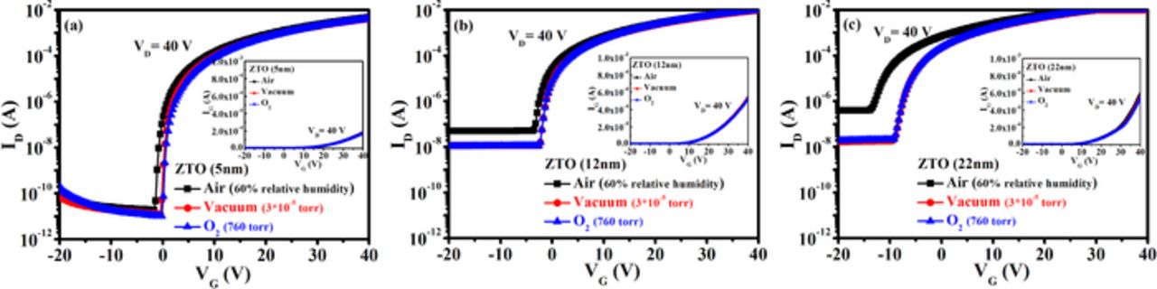
Figure 2. ID-VG transfer curves of ZTO TFTs with ZTO thickness of (a) 5, (b) 12 and (c) 22 nm measured under different atmospheres (air ambiance, vacuum and dry O2). The inset show the leakage current (IG) of three ZTO TFTs under different atmospheres.
Because the performances of oxide-based TFTs are strongly influenced by the degree of oxygen deficiency in the oxide active layers, we first characterize the oxygen deficiency in ZTO films by XPS. Figures 3a, 3b and 3c show O 1s XPS spectra of the 5, 12 and 22 nm-thick ZTO films. The spectra were obtained after a gentle sputtering cleaning (for 1 s only) to avoid the surface contamination. The core level electron binding energies have been calibrated for the charging effect with respect to the unintended C 1s peak at 285 eV. The O 1s peak is deconvoluted into three components: lattice oxygen in ZTO (530.4 eV, OI), oxygen nearby oxygen-deficient ZTO (532.1 eV, OII), and the oxygen bonds in the hydroxide (533.3 eV, OIII).3,21 The oxygen deficiency ratio is then defined as the peak area ratio of OII/(OI+OII+OIII). As a result, compared with the thicker ZTO films of 12 and 22 nm, the 5 nm-thick ZTO film had the largest oxygen deficiency due to easy out-diffusion of oxygen molecules (O2) from the ultra-thin solution processed film to the atmosphere when oxygen vacancies are created after high temperature annealing according to  .22–24
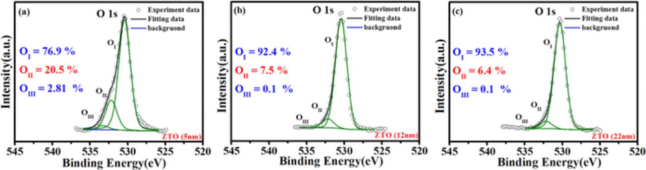
Figure 3. Deconvolution of the O 1s XPS spectrum of multiple spin-coated ZTO films with thickness of (a) 5, (b) 12 and (c) 22 nm.
Furthermore, the electronic structure of ZTO is examined by using UPS and the UPS spectra of three ZTO films are shown in Fig. 4. The photon energy is 21.2 eV. The Fermi energy (EF) was found by using the energy value at which the secondary cutoff region (Ecut-off) begins and adding to this the photon energy of 21.2 eV (i.e., EF = 21.2 - Ecut-off). On the other hand, the climb-up edge in UPS spectra of semiconductors corresponds to the energy difference between Fermi level and valence band edge (EV) (i.e., Eclimb-up = EV - EF). In addition, the optical bandgap energy (Eg) of ZTO film can be obtained from the absorption edge of the UV-Vis spectrum by using Tauc-plot analysis, and the resulting Eg is 3.7 eV, which is similar to the reported data for ZTO films.9,25–26 With the known Eg, the energy difference of Fermi-level to conduction band edge (i.e. EC - EF) for each individual ZTO film of 5, 12 and 22 nm is 0.82, 0.94 to 1.02 eV, respectively.
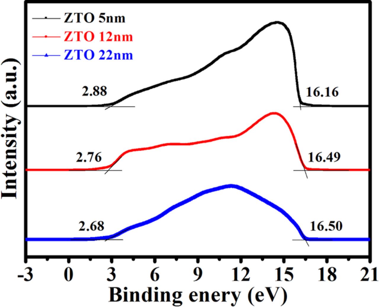
Figure 4. Ultraviolet photoemission spectroscopy (UPS) measurement of ZTO films thickness of 5, 12 and 22 nm.
Comparing XPS and UPS results, it is clear that oxygen vacancies in ZTO shall act as electron donors. As a consequence, the richest oxygen deficiency in the 5 nm-thick ZTO (Figs. 3a) leads to its highest volumetric carrier concentration (i.e. the smallest energy difference between EF and EC according to UPS analysis among three ZTO films. Similar to other impurity dopants, more oxygen vacancies produce higher carrier concentration but also induce more ionized impurity scattering. Therefore, μFE for 5 nm-thick ZTO TFT is the lowest among all. Furthermore, the Vth will be determined not only by semiconductor carrier density but also by the trapped charge density.27 Conducting electrons in the TFT channel will encounter trap states within active layer, at active layer/dielectric interface and deep energy level states of the dielectric. Therefore, to understand the carrier trapping during conduction for our ZTO TFTs, the time-dependent drain current (ID) and Vth as a function of stress time during the continuous bias stress of VG = 40 V, VD = 30 V for 2000 sec was measured. Figure 5a shows an ID vs. stress time graph for TFTs with various ZTO thicknesses. We calculated the drain current change percentage (ΔID (%)), which is defined as (IDbefore stress - IDafter stress)/ IDbefore stress × 100%. As a result, the ΔID value of the ZTO TFTs with thicknesses of 5, 12 and 22 nm were 26%, 5.9% and 0%, respectively. Similarly, as seen in Figure 5b, the Vth shift under bias stress (ΔVth = Vthafter stress - Vthbefore stress) is only 0.15 V for the 22 nm-thick ZTO TFT while it is about 2.66 V for the 5 nm-thick ZTO TFT. The 5 nm-thick ZTO TFT has the largest current decay and Vth shift as compared with others, which suggests that the charge carriers (i.e. electrons) are suffering from current crowding and carrier scattering from impurities/interface/surface at such a ultra-thin thickness. Therefore, the 5 nm-thick ZTO TFT exhibits the most positive Vth and lowest ID-off current although this ultra-thin ZTO film contains more oxygen vacancies. ID-off rises substantially for 12 nm- and 22 nm-thick ZTO TFTs, suggesting that the more carriers gathered up from the whole active layer thickness and most of carriers do not suffer from impurities/interface/surface scattering.
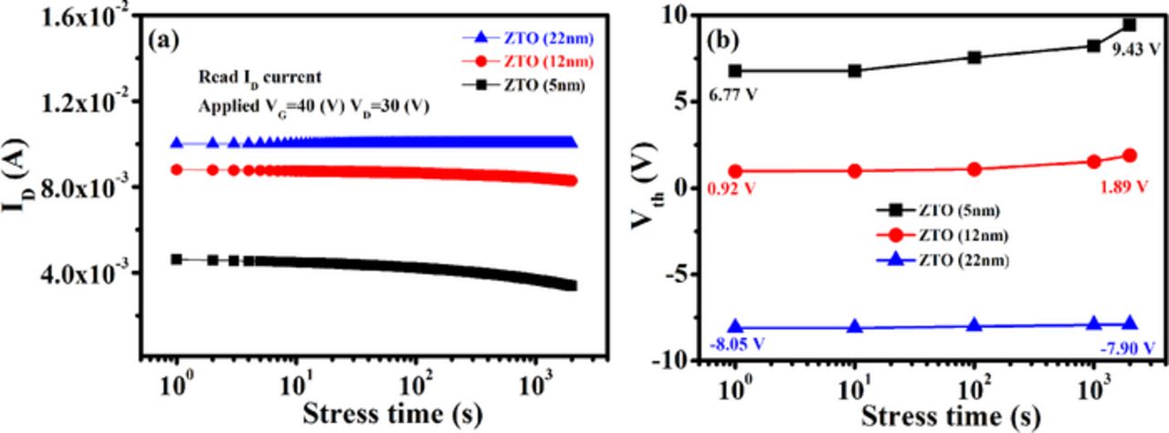
Figure 5. The evolution of (a) drain current (ID) and (b) threshold voltage (Vth) with stress time for a period of 2000 sec, in which VG = 40 V, VD = 30 V was continuously applied on the devices (5, 12 and 22 nm-thick ZTO TFTs).
Regarding to the ambiance stability, comparing to the data obtained under vacuum and dry O2, Vth of 12 nm- and 22 nm-thick ZTO TFTs measured in air shifts to negative direction and the ID-off increases (see Fig. 2 and Table I). In addition, we also measured positive/negative bias stress (PBS/NBS) in different ambiances for 5 nm-thick ZTO TFTs (see supplementary material, Fig. S1). This observation clearly indicates that adsorption of oxygen will not affect the ZTO TFT performance; nevertheless, as reported in the literature, water molecules in air (60% relative humidity) adsorbed on ZTO surface act as electron donors and consequently increase electron carriers in ZTO channel layers.19,28–29 On the other hand, the Vth and ID-off of 5 nm-thick ZTO TFT do not change apparently despite in air, dry O2 or vacuum. All three devices are not passivated on the back surface. Water adsorption on ZTO in air should also supply electrons to the 5 nm-thick ZTO layer; however, the ionized oxygen vacancies distributing through the 5 nm-thick ZTO may scatter away and/or recombine with electrons donated by water molecules. The combination of high oxygen vacancy concentration and ultra-thin thickness therefore make this 5 nm-thick ZTO TFT insensitive to ambiance (air vs. vacuum or dry O2), as well as maintain a substantially low ID-off to guarantee good performances for the 5 nm-thick ZTO TFT.
Conclusions
In this study, a moisture-imperious, passivation-free, solution-processed ZTO TFT is presented with an ultra-thin ZTO (5 nm-thick) active layer. This device performs a good mobility of 13∼14 cm2/Vs, as well as a small subthreshold swing (∼0.30 V/dec.) and high on/off current ratio (∼108), regardless of working in vacuum, dry O2 or moisture-contained air (60% relative humidity) ambiance. The superb ambient stability degrades if the ZTO thickness increases. According to XPS and UPS analyses on 5 nm- 12 nm- and 22 nm-ZTO films, oxygen vacancies are more abundant in the 5 nm-ZTO and acting as electron donors, leading to a high carrier concentration for the 5 nm-ZTO film, as compared to the other two. The high oxygen vacancy concentration prevents further electron donation from the moisture; as a result, the 5 nm-ZTO TFT preserves a good electrical stability in different ambiances. ID-off rises substantially for 12 nm- and 22 nm-thick ZTO TFTs, indicating that most of carriers do not suffer from impurities/interface/surface scattering. Therefore, by optimizing the active layer thickness with a proper oxygen vacancy concentration therein, we have demonstrated the potential of developing passivation-free, ambient-stable oxide TFTs by solution process.
Acknowledgments
The authors gratefully acknowledge the financial support from the Ministry of Science and Technology of Taiwan (grant No. MOST 104-2119-M-006-012-, MOST 102-2221-E-006-071-MY3 and MOST 103-2221-E-006-086-MY3).