
Abstract
Maskless H2SO4 wet-etching on sapphire substrates creates three-dimensional pyramidal pattern on sapphire surface. Alunogen self-forming mask grows in H2SO4 etching generating a dynamic self-masking action, which fabricates 3-dimensional pyramidal pattern on the etched sapphire wafers. The slope and size of the pyramids are controlled by rate ratio (k) between alunogen growth rate and c-plane etching rate. Constant k results in flat facet side-planes of sapphire pyramids and varying k in etching produce curved side-planes of the sapphire pyramid.

This is an open access article distributed under the terms of the Creative Commons Attribution 4.0 License (CC BY, http://creativecommons.org/licenses/by/4.0/), which permits unrestricted reuse of the work in any medium, provided the original work is properly cited.
Recently, PSS (patterned sapphire substrate) technology has been developed to promote the efficiency of high-brightness GaN-based LEDs.1 The patterned structure on the PSS wafers results in the lateral growth of GaN epitaxial layers, which reduces the threading dislocation density and improves the internal quantum efficiency. Also, the patterned structure on the PSS wafers enhances the light extraction efficiency by destroying the total internal reflection effect at the sapphire/GaN interface.2–7 Thus, the PSS technology enables the continuous improvement on both internal quantum efficiency (epitaxial quality) and light extraction efficiency of high-brightness GaN-based LEDs.8–10
Up to now, many approaches have been used to create the patterns on the sapphire wafers.5,11,12 Among them, the costly and tedious dry-etching process combined with the lithography technique is the most common method to produce PSS wafers.7 A reported simple wet-etching process has been demonstrated to produce PSS wafers without using any lithography and dry-etching processes.13–14 The PSS wafer fabricated by the simple wet-etching process is called nature patterned sapphire substrate (n-PSS). Four-side pyramids are the main pattern feature on the flat c-plane sapphire wafers. The pyramidal pattern created on the sapphire wafers is unique in two ways: firstly, the pyramids randomly formed on the sapphire substrate, i.e., with no relation respect to the crystallography of the sapphire wafer. The second unique point is that the slope of the four side-planes of pyramids is not flat. Instead, they are curved planes. So, the four side-planes of the pyramids on the n-PSS wafer are not any specific crystal planes of the sapphire wafer. The previous work by Liu and Chen has shown that the pyramid formed on the n-PSS is sapphire phase.15 Also, they proved that the sapphire pyramids on the n-PSS wafer improved the quality and efficiency of the GaN epi-layers on the n-PSS wafer. Yet, the previous research did not discuss the formation mechanism of the sapphire pyramids on the n-PSS wafers. With the detail formation mechanism of the sapphire pyramids on the etched sapphire wafer, the size and the shape of the pyramids on the n-PSS wafer can be manipulated to improve the efficiency of the GaN epi-layers.16 Therefore, the formation mechanism of pyramids on the n-PSS wafers is a critical issue to be studied.
Fig. 1(a) shows the SEM top-view image on the etched sapphire surface after the H2SO4-etching process at 240°C for 10 minutes. Cubic-like crystals can be observed on the etched sapphire surface. The cubic-like crystals have been identified to be alunogen (Al2(SO4)3·17H2O), which is the etching-reaction product formed during the etching process.15,17 The alunogen can be removed from the etched sapphire wafers by immersing the sapphire wafers in HCl solution at room temperature for 10 minutes. After removing the alunogen crystals by the dilute HCl acid solution, as shown in Fig. 1(b), sapphire pyramids are exposed on the etched sapphire wafers. Interestingly, we can see that the c-plane sapphire surface (the surface area other than the pyramids) of the etched sapphire wafer is very flat after the etching process. It means that the H2SO4 acid solution can etch the c-plane sapphire surface vertically and uniformly without creating any facet crystalline planes. Fig. 1(c) plots the average size of the sapphire pyramids versus the etching time. The average size of the sapphire pyramids increases with time. We used AFM to measure the roughness on the side-planes of the pyramid. The roughness (Ra) on the pyramids is less than 2 nm. To confirm the pyramids formed on the etched sapphire wafers, we prepared TEM sample at the location of “sapphire” pyramid. The TEM diffraction pattern at the location of “sapphire” pyramid, shown in Fig. 2, indicates that the sapphire pyramids are sapphire phase.
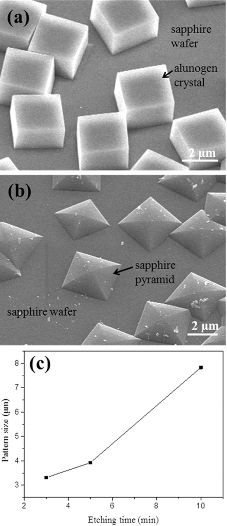
Figure 1. (a) alunogen crystals on the sapphire wafer. (b) sapphire pyramidal patterns on the etched sapphire wafers. (c) the average size of the sapphire pyramids versus the etching time.
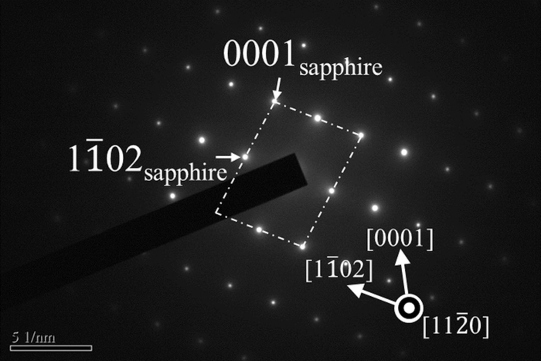
Figure 2. TEM diffraction pattern at the location of “sapphire” pyramid.
Typically, single-crystal materials are highly anisotropic in their properties. For example, with chemical wet etching, the crystal planes of a single-crystal material can be etched at very different rates. So, as a single-crystal material is etched with wet chemicals, the crystal planes with the slowest etching rate would dominate the appearance of the etched single-crystal material. In this work, the single-crystal sapphire wafer surely should show its anisotropic behavior under the chemical wet-etching process. Therefore, we would expect that the morphology of the sapphire pyramids on the etched sapphire wafer should be constructed by the specific crystal planes of the sapphire with the slowest etching rate. It is equivalent to saying that, the four side-planes and the location of the sapphire pyramids should have a specific relation with the crystallography of the sapphire wafer. Yet, as seen in the image in Fig. 1(b), we note that the sapphire pyramids randomly locate on the sapphire surface. Also, the side-planes of the sapphire pyramids are not flat facet surfaces. Instead, the side-planes of the sapphire pyramids are curved surface. It means that the position of the sapphire pyramids and the side-planes of the sapphire pyramids has no relation with the crystallography of the sapphire wafer. Thus, based on the above observations, we can conclude that the sapphire pyramids on n-PSS wafers are not created by the anisotropic etching with H2SO4 acid.
Here, we tend to believe that the formation of the sapphire pyramids on n-PSS wafers should relate to the growth process of the alunogen reaction-product during the H2SO4 etching process. Fig. 3(a) shows a close-up tiled SEM image on the alunogen reaction-product crystals on the etched sapphire surface. As seen in the bottom portion of Fig. 3(a), some alunogen reaction-product crystals were fallen off the etched sapphire surface. The exposed sapphire pyramids seemingly were covered by the alunogen reaction-product crystals during the etching process. Interestingly, as seen in Fig. 3(b), a flip-over alunogen reaction-product crystal is accidentally found next to a sapphire pyramid on the etched sapphire surface. Clearly, we can see that the inner shape of the flip-over alunogen reaction-product crystal exactly matches the outer shape of the adjacent sapphire pyramid. In addition, the bottom area of the sapphire pyramid well corresponds to the bottom area of the alunogen reaction-product crystal. We believe that the sapphire pyramid was originally covered by the flip-over alunogen reaction-product crystal. So, the morphology of the sapphire pyramids is likely shaped by the growth formation of the alunogen reaction-product crystal.
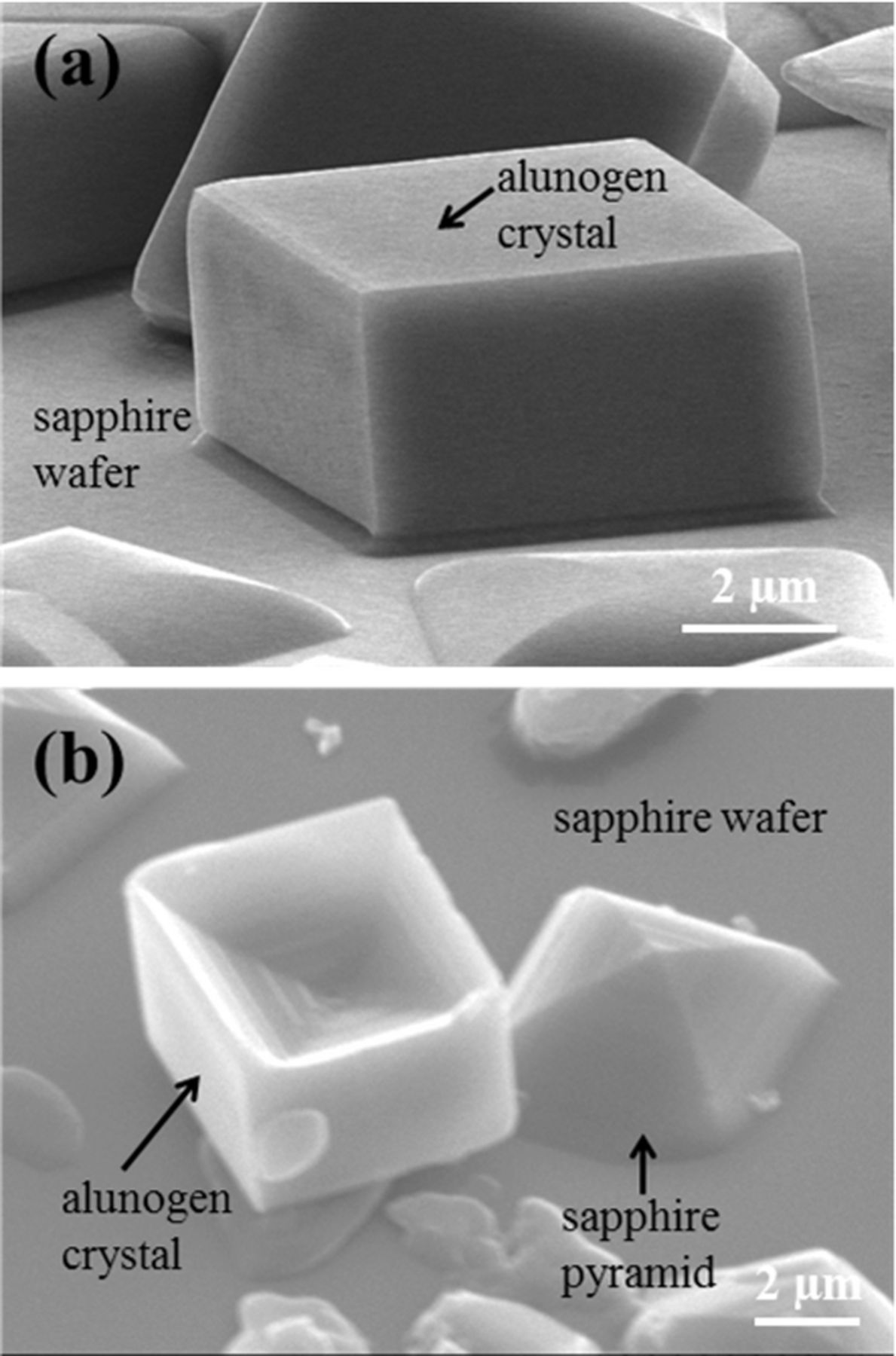
Figure 3. (a) close-up tilted view of the alunogen crystals. (b) a flip-over alunogen crystal next to a sapphire pyramidal pattern.
In the following, we will propose a formation mechanism of the sapphire pyramids on the etched sapphire wafer with H2SO4 wet-etching. Fig. 4 illustrates the formation evolution of a sapphire pyramid on the sapphire surface. Firstly, at the very beginning of the etching process, a thin surface layer on the sapphire wafer were etching by H2SO4. The etching reaction is shown in the Equation 1.18

Al3+ ions dissolved into the H2SO4 solution. Once the concentration of the dissolved Al3+ ions in the H2SO4 etching solution is saturated, the Al3+ ions would react with SO42− ions and form the alunogen (Al2(SO4)3·17H2O) nuclei on the sapphire surface, as shown in Fig. 4(a). The formation equation of the alunogen reaction-product crystal is expressed in the Equation 2.17

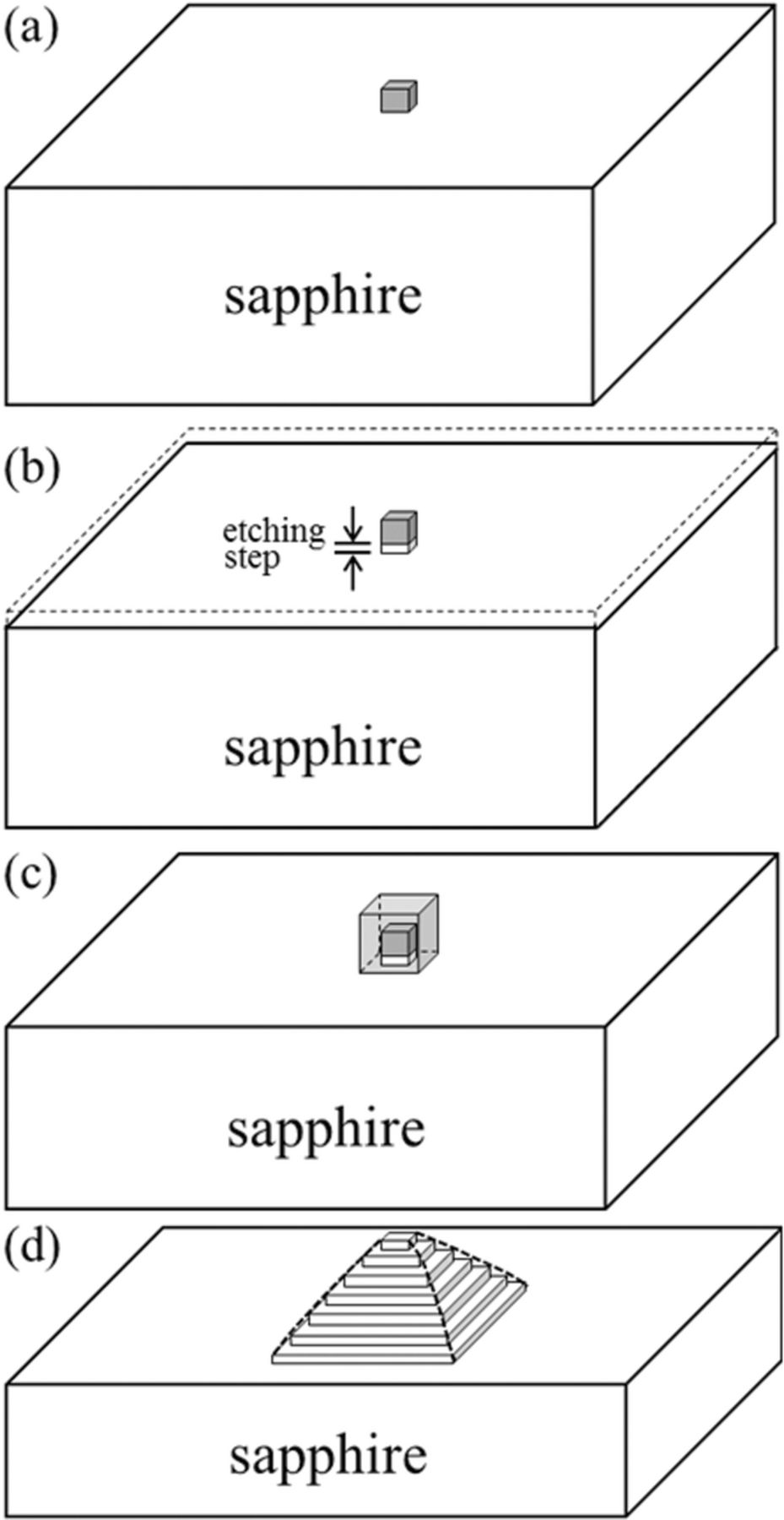
Figure 4. formation evolution of a sapphire pyramid on the sapphire surface.
The sapphire surface covered by the alunogen nuclei would be protected from being etching by H2SO4. Other sapphire surface area exposed to the H2SO4 etching solution would be etching down vertically with an etching rate (Rc) in the c-direction. As the exposed sapphire surface is etching down, a small etching-step would be created, as seen in Fig. 4(b). As the sapphire wafer is etching in the c-direction, more Al3+ ions would be releasing into the H2SO4 etching solution and leads to the growth of the alunogen nuclei. The growth rate of the alunogen nuclei is denoted as Rp. Then, the previous etching-step created by the vertical etching would be covered by the growing alunogen nuclei, as seen in Fig. 4(c). With the repetition of the etching processes of Fig. 4(b) and Fig. 4(c), i.e., the c-direction etching and the alunogen growth, the sapphire pyramids would be created on the etched sapphire surface, as shown in Fig. 4(d). The alunogen nuclei could nucleate on the sapphire surface with any orientation, i.e., no relation with the crystallography of the sapphire wafer. That explains why the sapphire pyramids formed randomly on the etching sapphire surface.
As seen in Fig. 3(b), the side-planes of sapphire pyramids appear smoothly in SEM image. It means that the etching-step caused by the vertical etching (Rc) is very small during the etching process. Yet, in some special etching condition (etching in lower temperature like 220°C), as shown in Fig. 5, the stepped surface can be clearly observed on the side-planes of sapphire pyramids. We believe that the stepped surface is caused due to the discontinuity of the c-plane etching or the alunogen growth in the etching processes. We note that a saturation concentration of Al3+ ions in the etching solution should be met for the growth of the alunogen nuclei. Therefore, if an incubation time needs to be taken to reach the saturation concentration of Al3+ ion in the etching solution, the growth of alunogen nuclei could be discontinuous. The discontinuous growth of Alunogen nuclei results in the stepped surface on the side-planes of sapphire pyramids.
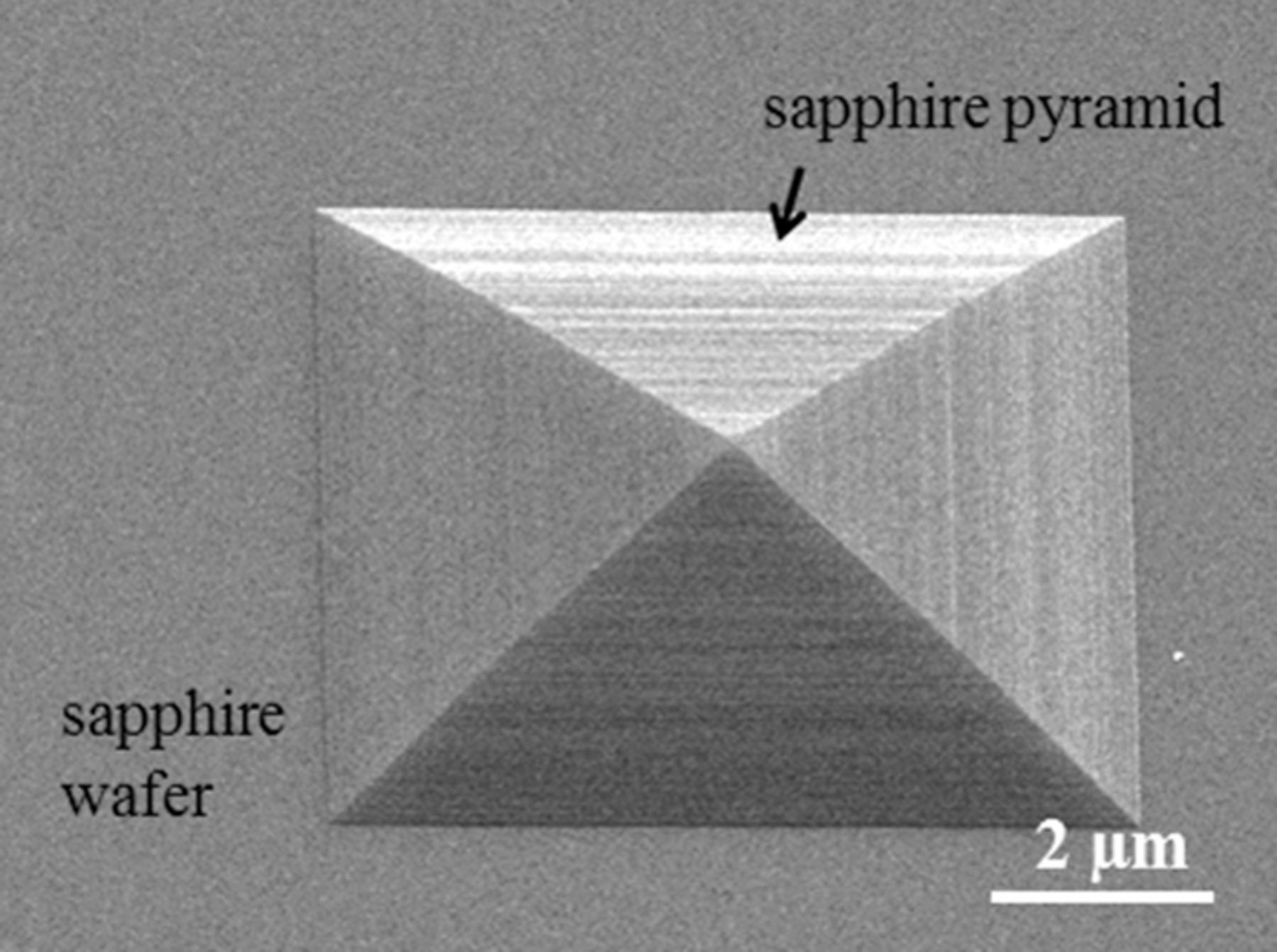
Figure 5. a sapphire pyramid with stepped surface on the side-planes.
Moreover, based on the formation mechanism discussed above, the slope of the side-planes of the sapphire pyramids should depend on the rate ratio (k = Rp/Rc) between the alunogen growth rate (Rp) and the c-direction etching rate (Rc). If the alunogen growth rate and the c-direction etching rate are kept as constant over the etching period, the slope of the side-planes of sapphire pyramids would be constant and result in flat side-planes. The flat side-planes of a sapphire pyramid can be seen in Fig. 5. So, the magnitude of k defines the slope of the flat side-planes of the sapphire pyramids. The larger k value (with a faster alunogen growth rate) would result in the flater side-planes. On the contrary, a smaller k (with a faster c-direction etching rate) would cause the steeper side-planes of sapphire pyramids. If k value varies with the etching time, the slope of the side-planes of sapphire pyramids would change over the etching time. Consequently, curved side-planes would be resulted. This happens for most etching conditions at 240°C. The curved side-planes of the sapphire pyramid can be seen in Fig. 1(b). The slope of the side-planes in the upper portion of sapphire pyramids is smaller than the slope of the side-planes of the bottom portion of the sapphire pyramids. It implies that the alunogen growth rate is larger in the initial etching and slows down in the late stage of etching.
In conclusion, maskless wet-etching on sapphire substrates using H2SO4 etching causes pyramidal pattern on sapphire surface. The pyramidal pattern is attributed to the formation of the alunogen compound crystal functioning as self-forming mask on the sapphire surface during etching. The alunogen self-forming mask grows with the etching time that generates a dynamic self-masking action. The act of the time-varying and self-masking alunogen crystal creates the 3-dimension etching morphology, which is pyramidal pattern on the etched sapphire wafers.
The formation mechanism of the sapphire pyramids on the etched sapphire wafer with H2SO4 wet-etching is proposed in this work. The slope and size of the pyramids are controlled by rate ratio (k) between the alunogen reaction-product growth rate and the c-plane etching rate. If k is constant, the slope of the four side-walls of sapphire pyramids would be a constant. If k varies with the etching time, the side-planes of the sapphire pyramid curved.
Acknowledgment
This work was supported by the Ministry of Science and Technology Grant 101 2221-E-008-036-MY3, and Energy Technology Program, Ministry of Science and Technology Grant 104-ET-E-008-002-ET.