
Abstract
We developed V-doped In2O3 (IVO) films to use as a buffer- and anode-integrated electrode for acidic poly (3,4-ethylene dioxylene thiophene):poly (styrene sulfonic acid) (PEDOT:PSS) buffer layer free-organic solar cells (OSCs). By co-sputtering of V2O5 and In2O3 targets and rapid thermal annealing, we obtained IVO films with a sheet resistance of 41.7 Ω/square, and an optical transmittance of 80.4%, and a work function of 5.0 eV. The P3HT:PCBM-based OSCs fabricated on an IVO anode successfully functioned without an acidic PEDOT:PSS buffer layer and showed a PCE of 2.91%, which was much higher than that (1.068%) of a PEDOT:PSS free OSC with an ITO anode. The elimination of the acidic buffer layer in OSCs enabled us to produce the reliable OSCs with decreased coating steps.
Cost-effective and simply fabricated organic solar cells (OSCs) are considered as renewable and eco-friend energy sources.1,2 For high-performance of OSCs, chemically stable transparent anodes are very important because transparent anodes directly contact an acidic poly (3,4-ethylene dioxylene thiophene):poly (styrene sulfonic acid) (PEDOT:PSS) buffer layer in conventional OSC structures.3 Although sputtered Sn-doped In2O3 (ITO) films have been widely employed as transparent anodes in OSCs due to their low resistivity and high transparency, mismatched band alignment between the ITO anode and the polymer active layer requires an additional acidic PEDOT:PSS buffer layer to increase the hole extraction efficiency.4 However, the acidic PEDOT:PSS buffer layer critically affects the stability and life-time of OSCs because the acidic PEDOT:PSS buffer layer leads to etching of the ITO anode and diffusion of indium into the organic layer.5,6 As an alternative to the acidic PEDOT:PSS buffer layer, V2O5 films have been reported as a effective buffer layer between ITO and the polymer active layer. Shrotriya et al. reported that the power conversion efficiency (PCE ∼ 3.10%) of OSCs with 3 nm-thick V2O5/ITO electrode is similar to that (3.18%) of OSCs with PEDOT:PSS/ITO electrodes.7 Hancox et al. also reported that evaporated V2O5 layer effectively acts as a hole transport layer due to its high work function of 6.8 eV.8 However, additional coating of a V2O5 buffer layer on the ITO anode increases the OSC fabrication steps and generates additional interfaces including V2O5/polymer active layer and V2O5/ITO anode. Although several concepts for PEDOT:PSS-free OSCs including inverted OSCs have been suggested,9,10 the buffer- and transparent anode-integrated electrode is another effective method to eliminate the use of acidic PEDOT:PSS buffer layer, as we suggested in our previous works.11,12 In this letter, we developed acidic PEDOT:PSS buffer-free OSCs using V-doped In2O3 (IVO) films. By co-sputtering of V2O5 and In2O3 targets and effective rapid thermal annealing for V dopant activation and crystallization of IVO films, we fabricate crystalline IVO electrodes, which simultaneously act as buffer and anode layers. By comparing the performance of acidic PEDOT:PSS-free OSCs with IVO and reference ITO anodes, we demonstrated the potential of the IVO film as a buffer- and anode-integrated electrode for PEDOT:PSS-free OSCs.
By co-sputtering of V2O5 and In2O3 targets, 200 nm-thick IVO films were deposited on a 15 × 15 mm2 glass substrate at room temperature. The IVO films were grown at a constant DC power of 100 W applied to the In2O3 target, a RF power of 10 W applied to the V2O5 target, an Ar flow rate of 10 sccm, a working pressure of 3 mTorr and a deposition rate of 0.3 nm/sec. The co-sputtered IVO films were then rapidly thermal annealed at 500 and 600°C under 10−3 Torr for 10 min using a rapid thermal annealing (RTA) system. The electrical and optical properties of the IVO films were analyzed by means of Hall effect measurements and an UV/visible spectrometer as a function of annealing temperature. The microstructure of the annealed IVO films was examined by synchrotron X-ray scattering and high resolution transmission electron microscopy (HRTEM: JEM-2100F). The possibility of using an IVO film as an anode for conventional P3HT:PCBM-based OSCs and a buffer- and anode-integrated electrode for PEDOT:PSS-free OSCs was investigated by comparing the performance of OSCs with IVO and reference ITO electrodes. To fabricate conventional OSCs on the IVO and reference ITO electrodes, PEDOT:PSS (Clevios PH 510, H. C. Starck) was spin-coated onto the electrode substrates and subsequently annealed at 120°C for 10 min. A blend solution of 50 mg P3HT (Rieke Metals) and 50 mg PCBM (Nano-C) in 2 mL of o-dichlorobenzene (o-DCB) was spin-coated on the IVO and ITO electrodes in a nitrogen environment. A solvent annealing treatment was then performed for 120 min while keeping the photoactive films inside a covered glass jar. Each sample was subsequently annealed at 110°C for 10 min. In case of PEDOT:PSS-free OSCs, the P3HT:PCBM active layer was directly coated on the IVO and ITO electrodes, respectively without coating of the PEDOT:PSS layer. Finally, a Ca/Al (20/100 nm) cathode with an area of 4.66 mm2 was deposited on the photoactive layer via thermal evaporation. The cathode layer was patterned by a thin shadow mask. The photocurrent density-voltage (J-V) curves of the OSCs fabricated on the IVO and ITO electrodes were measured with a Keithley 1200 measurement unit under 100 mW/cm2 illumination and AM 1.5 G conditions. A reference Si solar cell certified by the International System of Units (SI) (SRC 1000 TC KG5 N, VLSI Standards, Inc) was employed to ensure accurate measurements.
Figures 1a and 1b show the Hall measurement results of the as-deposited and 500 and 600°C-annealed IVO films. Sheet resistance and resistivity of the IVO films decreased with increasing RTA temperature. The as-deposited IVO film exhibited a fairly high sheet resistance of 231.1 Ω/square and a resistivity of 4.62 × 10⁻³ Ω-cm due to insufficient activation of V dopants in the In2O3 matrix. However, the annealed IVO films showed significantly decreased resistivity. At a 600°C of RTA temperature, the IVO films exhibited the lowest sheet resistance of 41.7 Ω/square and a resistivity of 8.36 × 10⁻⁴ Ω -cm. The reduced resistivity of the annealed IVO film with increasing RTA temperature was attributed to an increase in carrier concentration, as shown in Figure 1b. Due to effective substitution of V5+ dopant with In3+ sites and generation of excess electrons in the In2O3 matrix during the RTA process, the annealed IVO film showed high carrier concentration. Figure 1c shows the optical transmittance of the IVO films as a function of RTA temperature. All IVO films showed similar optical transmittance in the visible wavelength region regardless of RTA temperature. The 600°C-annealed IVO film showed a higher optical transmittance of 80.4% at a 550 nm wavelength and an average transmittance of 88.9% between 400 nm and 800 nm. The inset picture in Figure 1c shows similar optical transparency of as-deposited and annealed IVO films. Figure 1d shows the figure of merit (FOM = Rsh/T10) values obtained from the sheet resistance (Rsh) and optical transmittance (T) of the IVO films as a function of the RTA temperature.13 Due to similar optical transmittance of as-deposited and annealed IVO films, the FOM value is mainly dependent on the Rsh value of the IVO films. Therefore, the 600°C-annealed IVO films showed the highest FOM value of 2.76 × 10⁻³ Ohm−1, which is comparable to crystalline-ITO films.13
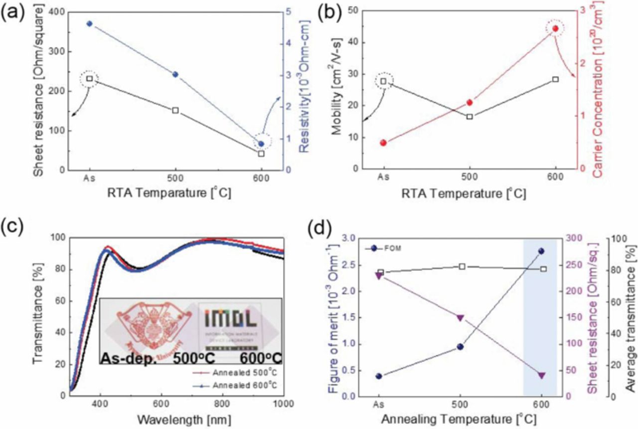
Figure 1. (a) Resistivity and sheet resistance of the IVO films as a function of the RTA temperature. (b) Mobility and carrier concentration of IVO films with increasing RTA temperature. (c) Optical transmittance of the IVO films as a function of RTA temperature Inset pictures show the picture of the as-deposited and annealed IVO films. (d) Figure of merit values of the IVO films calculated from the sheet resistance (Rsh) and transmittance at 550 nm (T).
Figure 2a showed synchrotron XRS plots of the IVO films as a function of RTA temperature. The as-deposited IVO films exhibited broad amorphous and crystalline overlapping peaks because the co-sputtering process occurs at room temperature. With increasing RTA temperature, the intensity of the (222) peak increased due to crystallization of the IVO film with a bixbyite structure.14 The XRS results for the 600°C-annealed IVO films showed several strong peaks including (211), (222), (400), (440) and (622) at 2θ = 22.02°, 30.88°, 35.74°, 51.56° and 60.96° respectively. Due to substitution of V5+ ions with a radius of 0.79Å for In3+ ions with a radius of 0.80Å, the (222) peak shifted to a higher angle due to shrinkage of the bixbyite lattice.14 Figure 2b showed the surface FE-SEM images of as-deposited and 600°C-annealed IVO films. Compared to as-deposited IVO films, the 600°C-annealed IVO films had larger grain sizes due to crystallization of IVO. The cross-sectional TEM image in Figure 2c clearly shows that the 600°C-annealed IVO film had a vertical columnar structure in the [00-2] direction normal to the interface, as expected from XRS results. The 600°C-annealed IVO film showed a rectangular shaped columnar structure with a size of 50-67 nm. Enlarged HRTEM images in Figure 2d obtained from the middle region of the IVO film demonstrate that the 600°C-annealed IVO film had a good crystallinity with a bixbyite structure similar to conventional ITO films. In addition, strong spots in the Fourier transformation (FFT) patterns in the inset confirm the good crystallinity of the 600°C annealed-IVO film.
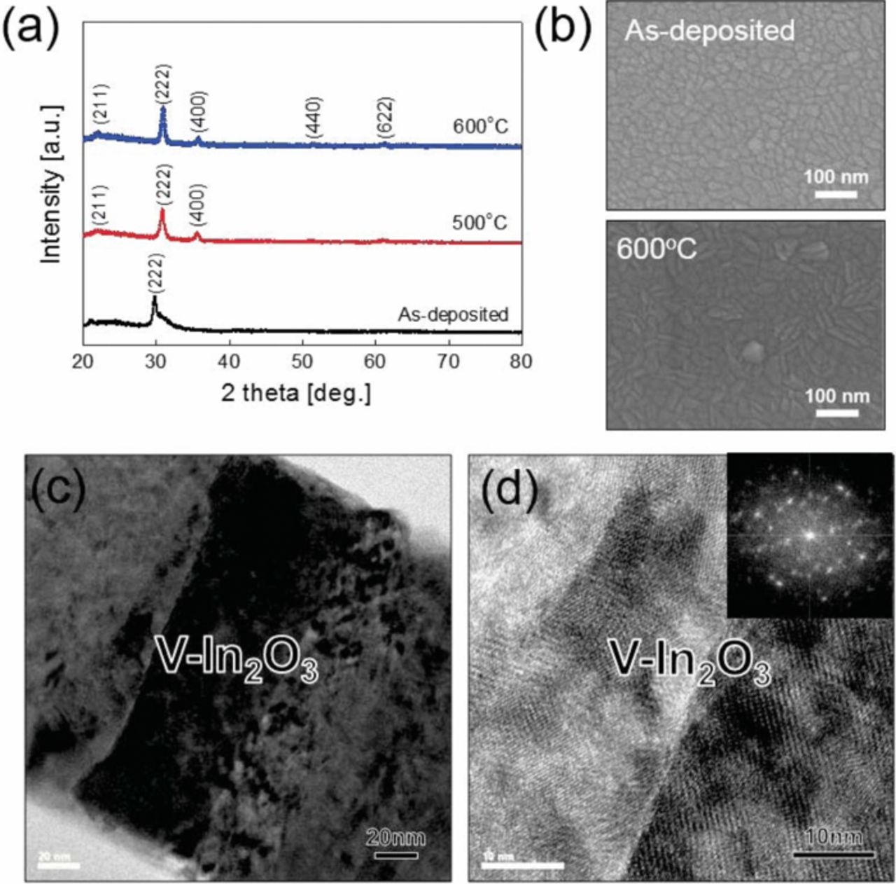
Figure 2. (a) Synchrotron X-ray scattering plots and (b) surface FESEM images for the as-deposited and 600°C-annealed IVO films. (c) Cross-sectional TEM image of the IVO film with very smooth surface morphology. (d) Enlarged TEM image of annealed IVO films with an inset of the FFT pattern.
Figure 3a shows the photocurrent density-voltage (J-V) curves for PEDOT:PSS-based OSCs fabricated on the IVO and reference ITO anodes. The inset picture shows the OSCs cell fabricated with an IVO anode. The PEDOT:PSS-based OSCs fabricated on the reference ITO anode exhibited the following cell performance in Figure 3a : a FF of 64.56%, a Jsc of 9.723 mA/cm2, a Voc of 0.603 V, and a PCE of 3.783%. The OSC with an annealed IVO anode showed a similar PCE due to high optical transmittance and low sheet resistance. The energy level band diagram of OSCs with IVO and ITO anodes are illustrated in Figure 3b. The work functions of annealed IVO (5.0–5.1 eV) and ITO (4.6 eV) were investigated using a Kelvin probe measurement. Due to the existence of a conductive PEDOT:PSS buffer layer, which acts as an ohmic contact layer, the OSCs on annealed IVO and reference ITO showed similar performances, as summarized in Table I. Figure 3c shows the J-V curves for PEDOT:PSS-free OSCs fabricated on reference ITO and IVO films. Detailed performance parameters are also summarized in Table I. The PEDOT:PSS-free OSCs with a reference ITO anode showed very poor cell-performance, a FF of 25.42%, a Jsc of 8.763 mA/cm2, a Voc of 0.479 V, and a PCE of 1.068%, because effective hole extraction from the organic active layer could not occur without a PEDOT:PSS buffer layer.15 As shown in the energy level diagram (Figure 3d), the high energy level mismatch between the ITO and the highest occupied molecular orbital (HOMO) of the P3HT led to poor hole extraction for the ITO anode. However, the OSCs fabricated on the annealed IVO films exhibited better cell-performance: an average PCE of 2.72%, an average Voc of 0.52 V, an average FF of 56.09%, and an average Jsc of 9.66 mA/cm2. Such performance is comparable to that obtained for IVO-based OSCs with a PEDOT:PSS layer. The successful operation of PEDOT:PSS free-OSCs on the annealed IVO films was attributed to the well matched work function of IVO with the P3HT:PCBM active layer, as shown in Figure 3d. Due to the high work function of V2O5 mixed in the In2O3 films, the hole generated in the P3HT:PCBM layer was effectively extracted from the active layer to the IVO anode. As reported by Hancox et al., the introduction of solution-processed vanadium oxide with a high work function (5.6 eV) effectively extracts the hole carrier from the active layer without need for a PEDOT:PSS buffer layer.8
Table I. Comparison of the performances of heterojunction organic solar cells fabricated on reference ITO and IVO electrodes with and without a PEDOT:PSS.
| VOC [V] | JSC [mA/cm2] | FF [%] | PCE [%] | |
|---|---|---|---|---|
| ITO-PEDOT | 0.603 ± 0.001 | 9.723 ± 0.023 | 64.56 ± 0.05 | 3.783 ± 0.010 |
| 500°C IVO-PEDOT | 0.576 ± 0.004 | 9.664 ± 0.039 | 62.53 ± 0.02 | 3.482 ± 0.051 |
| 600°C IVO-PEDOT | 0.557 ± 0.001 | 9.498 ± 0.067 | 65.52 ± 0.09 | 3.469 ± 0.097 |
| ITO-PEDOT free | 0.479 ± 0.027 | 8.763 ± 0.020 | 25.42 ± 0.18 | 1.068 ± 0.030 |
| 500°C IVO PEDOT free | 0.537 ± 0.007 | 9.831 ± 0.090 | 47.96 ± 0.19 | 2.534 ± 0.008 |
| 600°C IVO-PEDOT | 0.509 ± 0.012 | 9.495 ± 0.060 | 60.22 ± 0.19 | 2.910 ± 0.027 |
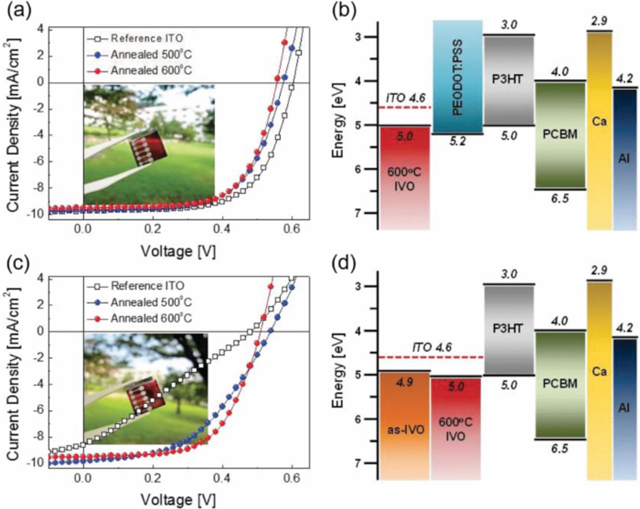
Figure 3. (a) Photocurrent density-voltage (J-V) curves and (b) energy level diagram for PEDOT:PSS-based OSCs with IVO and reference ITO electrodes. (c) J-V curves and (d) energy level diagram for PEDOT:PSS-free OSCs with IVO and reference ITO anode.
Figure 4a shows a cross-sectional TEM images of the PEDOT:PSS-based OSC and PEDOT:PSS free-OSCs fabricated on the 600°C-annealed IVO film. The cross-sectional TEM image clearly shows a well-defined crystalline IVO anode, a PEDOT:PSS buffer layer, a P3HT:PCBM active layer, and a Ca:Al cathode layer. It was clearly shown that the surface of the IVO anode was fairly rough due to interfacial reaction with the acidic PEDOT:PSS layer. As discussed by Jong et al., PEDOT:PSS on the ITO anode led to diffusion of indium into the PEDOT:PSS layer, which resulted in chemical degradation of the ITO anode.6 Figure 4b shows enlarged the HRTEM images obtained from the interface between the IVO anode and acidic PEDOT:PSS buffer layer. The rough surface and formation of an interfacial layer (mixed region) indicate the interfacial reaction between IVO and acidic PEDOT:PSS. However, a cross-sectional TEM image obtained from PEDOT:PSS-free OSC in Figure 4c exhibits a well-defined clean interface between the IVO and P3HT:PCBM layer due to the absence of an interfacial reaction. Figure 4d shows the enlarged image of the interface between the IVO film and P3HT:PCBM active layer. Due to the absence of an acidic PEDOT:PSS layer, the surface of the IVO anode was in good contact with the P3HT:PCBM layer without an interfacial reaction. Due to the high work function of IVO and the clean interface, the hole carriers generated in P3HT:PCBM were effectively extracted through the IVO layer without a PEDOT:PSS buffer layer.
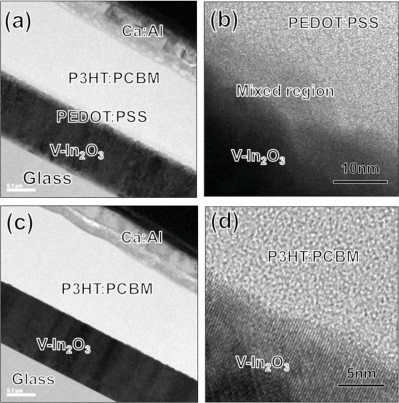
Figure 4. (a) Cross-sectional TEM image of the PEDOT:PSS based-OSC and (b) interface region between IVO and PEDOT:PSS buffer layer. (c) Cross-sectional TEM image of PEDOT:PSS-free OSC with IVO anode. (d) HRTEM images of the interface between P3HT:PCBM and the IVO electrode.
In conclusion, we report buffer- and anode-integrated IVO films prepared by co-sputtering for PEDOT:PSS-free OSCs. The optimized IVO film showed a sheet resistance of 41.7 Ohm/square, a transmittance of 80.39%, and a work function of 5.0 eV, comparable to a conventional ITO anode. Due to the existence of V2O5 in the In2O3 matrix, the IVO electrode showed a higher work function (5.0–5.1 eV) than the conventional ITO film (4.6 eV). Using the buffer- and anode-integrated IVO film, we fabricated a PEDOT:PSS free-OSC with a PCE of 2.910%, which is higher than that of a PEDOT:PSS free-OSC fabricated on a commercial ITO anode (1.068%). This result indicates that transparent IVO electrodes can simultaneously act as a buffer and an anode layer and can be considered as promising transparent electrodes for cost-efficient and reliable OSCs due to elimination of acidic PEDOT:PSS buffer layer.
Acknowledgments
This work was supported by New and Renewable Energy Program of the Korea Institute of Energy Technology Evaluation and Planning (KETEP) funded by the Korea government Ministry of Trade, industry & Energy (20113010010030).