
Abstract
We demonstrate thin body GeOI Pseudo-MOSFETs fabricated by a novel GeOI fabrication process based on epitaxial Ge films grown on III-V compound semiconductor wafers and wafer bonding. Ge surfaces before bonding are treated by plasma post oxidation to form GeOx, which can provide better interfacial quality between Ge and buried oxides. Normal operations of n- and p-MOSFETs are confirmed for GeOI with average thickness of 60 to 20 nm. The peak effective hole and electron mobility of 122 and 235 cm2/Vs, respectively, have been obtained for 20-nm-thick-GeOI n- and p-MOSFETs. The GeOI thickness dependence of mobility is also examined.

This is an open access article distributed under the terms of the Creative Commons Attribution 4.0 License (CC BY, http://creativecommons.org/licenses/by/4.0/), which permits unrestricted reuse of the work in any medium, provided the original work is properly cited.
Silicon (Si) large-scale integrated (LSI) circuit technologies have been widely developed over 40 years. However, they are now facing to the scaling limit of metal oxide semiconductor field effect transistors (MOSFETs).1,2 To breakthrough this critical issue, new structures and materials alternative to conventional bulk-Si MOSFETs have recently been proposed to be applied to the channel layers in complementary metal oxide semiconductor (CMOS) fabricated on the Si platform. One promising approach is the integration of germanium (Ge) as a MOSFET channel material.3–6 Recently, Ge p-MOSFETs and n-MOSFETs with high peak mobility and thin equivalent oxide thickness (EOT) have been demonstrated by employing high quality GeOx/Ge interfaces in the gate stack.7–11 Also, ultrathin body (UTB) Ge-on-insulator (GeOI) structures are strongly needed to enhance the immunity against short channel effects, which is mandatory for scaled MOSFETs.12 However, the effective mobility of MOSFETs on GeOI wafers fabricated by Smart Cut has been reported to be lower than expected for the Ge thickness less than 20 nm,13,14 which might be caused by crystal defects near the Ge/buried oxide (SiO2) interfaces generated during the GeOI fabrication process, and/or some residual damages originating from hydrogen implantation.15,16 Therefore, high quality GeOI substrate formation is a key to realize good performance in UTB GeOI devices.
In this paper, a novel way to fabricate GeOI substrates, based on the transfer of Ge layers epitaxially grown on III-Vs, has been demonstrated. The transfer technique of similar Ge layers on III-Vs has been reported by using epitaxial lift-off (ELO).17 On the other hand, the present method allows us to realize wafer-level GeOI formation with uniform interface control with buried oxide (BOX) insulator layers. The back interface quality of GeOI structures is quite important particularly for carrier transport properties in ultrathin GeOI layer.18 In this study, GeOx/Ge interfacial layers were applied to the Ge/buried oxide Al2O3 interfaces in order to improve the back interface properties. By using the GeOI structures fabricated by the present method, we fabricated MOSFETs with the GeOI thickness down to 20 nm and studied the electrical characteristics. Furthermore, the effective electron and hole mobility of the GeOI MOSFETs was systematically examined with reducing the GeOI thickness.
An n-type Ge layer for GeOI channel fabrication was epitaxially grown on 4-inch Gallium Arsenide (GaAs) substrates with 5 nm Aluminum Arsenide (AlAs), because the lattice constant of Ge is almost the same as those of GaAs and AlAs.19 An Indium Gallium Phosphide (InGaP) layer with the lattice constant similar to that of Ge was introduced between Ge and the GaAs substrate as an etching stop layer during transferring the Ge layer to a Si substrate. Figure 1a shows the result of a secondary ion mass spectroscopy (SIMS) analysis of a 700 nm-thick (100)-oriented Ge layer donor wafer. It is observed that As and Ga atoms are incorporated into the Ge epitaxial layer. Since the concentration of As is higher than that of Ga, the Ge layer can be regarded as n-type with the average donor concentration of around 2 × 1017 cm−3.
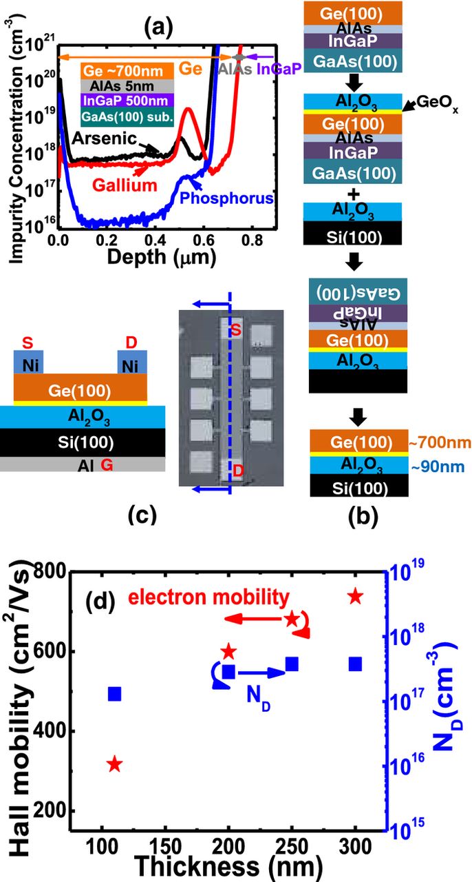
Figure 1. (a) Schematic cross-section and SIMS profile of epitaxial Ge on GaAs substrate. The concentration of the other dopants is under the detection limit. (b) Process flow of GeOI wafer fabrication. (c) Schematic and microscopic image from the top view of a back gate MOSFET device on GeOI substrate. The size of MOSFET is W/L = 100 μm / 500 μm. (d) Hall mobility and carrier concentration in Vg = 0 of the GeOI back gate device, Ge layer thicknesses range from 110 nm to 300 nm.
The process flow of the GeOI substrates fabrication is shown in Figure 1b. After surface pre-cleaning, Al2O3 was deposited on the donor wafer by atomic layer deposition (ALD) in two steps, as follows. 1-nm-thick Al2O3 was deposited first to cover the surface and then electron cyclotron resonance (ECR) plasma post oxidation10 was applied to form GeOx/Ge interfaces for achieving the good back interfacial properties after bonding. After that, 90-nm-thick Al2O3 was deposited after plasma post oxidation as the second steps. In order to make the manual boding in air easier, chemical mechanical polishing (CMP) was conducted after Al2O3 deposition. Then the donor wafer was bonded with a Si handle wafer with deposited 10 nm-thick Al2O3, followed by annealing at 350°C for 1 hour with 1500 N pressure. This temperature is low enough to keep BOX intact and prevent generation of any damages to the GeOI layer. After thinning the GaAs substrate down to less than 100 μm by polishing, GaAs was selectively etched against the InGaP etch stop layer by a H3PO4 /H2O2/H2O solution for about 30 min. The etching stop InGaP and AlAs layers were selectively etched against the Ge layer by HCl and HF solutions, respectively. The thickness of the Al2O3 BOX layer, measured by spectroscopic ellipsometry, was around 90 nm.
By using the newly fabricated GeOI substrates, back gate MOSFETs with metal source/drain (S/D) were fabricated with different Ge thicknesses. The thickness of the GeOI layer was around 700 nm after removal of the III-V semiconductor layers, and then the Ge layers were thinned by reactive ion etching (RIE) with CF4 down to less than 100 nm. Further thinning was done by wet etching in a H2SO4/H2O2/H2O diluted solution. By careful control of the etching time, the average thickness of Ge could be reduced down to 20 nm with root mean square (RMS) of surface roughness of ∼0.72 nm, measured over an area of 10 × 10 μm2 by atomic force microscopy (AFM). After mesa structures patterned by wet etching, Nickel (Ni) and Al were thermally evaporated to form electrodes and back gate contact, respectively. Here, the thicknesses of GeOI were varied by different etching time and estimated by surface step measurements after isolation mesa etching, and finally calibrated by using the thickness of the thinnest sample measured by cross-sectional TEM. The schematic structure and the microscopic image from top-view of the fabricated devices with Hall bars are shown in Figure 1c. The devices allow us to conduct Hall measurements and 4-point resistance measurements for subtracting the S/D contact resistance. The channel width/length (W/L) was 100 μm/500 μm.
In order to evaluate the quality and doping concentration of the bonded Ge layers, the Hall measurement was applied to the GeOI structures with the thick Ge layers. Figure 1d shows the Hall measurement results of GeOI with the Ge thickness ranging from 110 nm to 300 nm at Vg = 0 V. The electron concentration derived from the Hall measurement is around 2 × 1017 cm−3, which matches the results of the SIMS profiles of the as-grown epitaxial Ge wafer, shown in Figure 1a. The Hall mobility is higher than 300 cm2/Vs in GeOI with the average thickness of 110 nm. Although the Hall mobility is relatively low in comparison with that of n-type bulk Ge with the same impurity concentration, which is over 2000 cm2/Vs,20 the GeOI layer quality is acceptable for MOSFET application.
We evaluated the electrical properties of the fabricated thin body GeOI MOSFETs with the average GeOI layer thickness down to 20 nm. Figure 2a and 2b show the transfer characteristics (Id-Vg) and output characteristics (Id-Vd), respectively, of 20 nm-thick GeOI p-MOSFETs with the channel width/length of 100 μm/500 μm. The normal p-MOSFETs operation of thin body GeOI is confirmed. The Vth shift among different Vds might originate in the junctionless structure. Since the source and drain are un-doped and no p-n junctions are included in the devices, the drain bias could be shielded by any reversed p-n junction, but could directly change the surface potential near the source region to some extent.
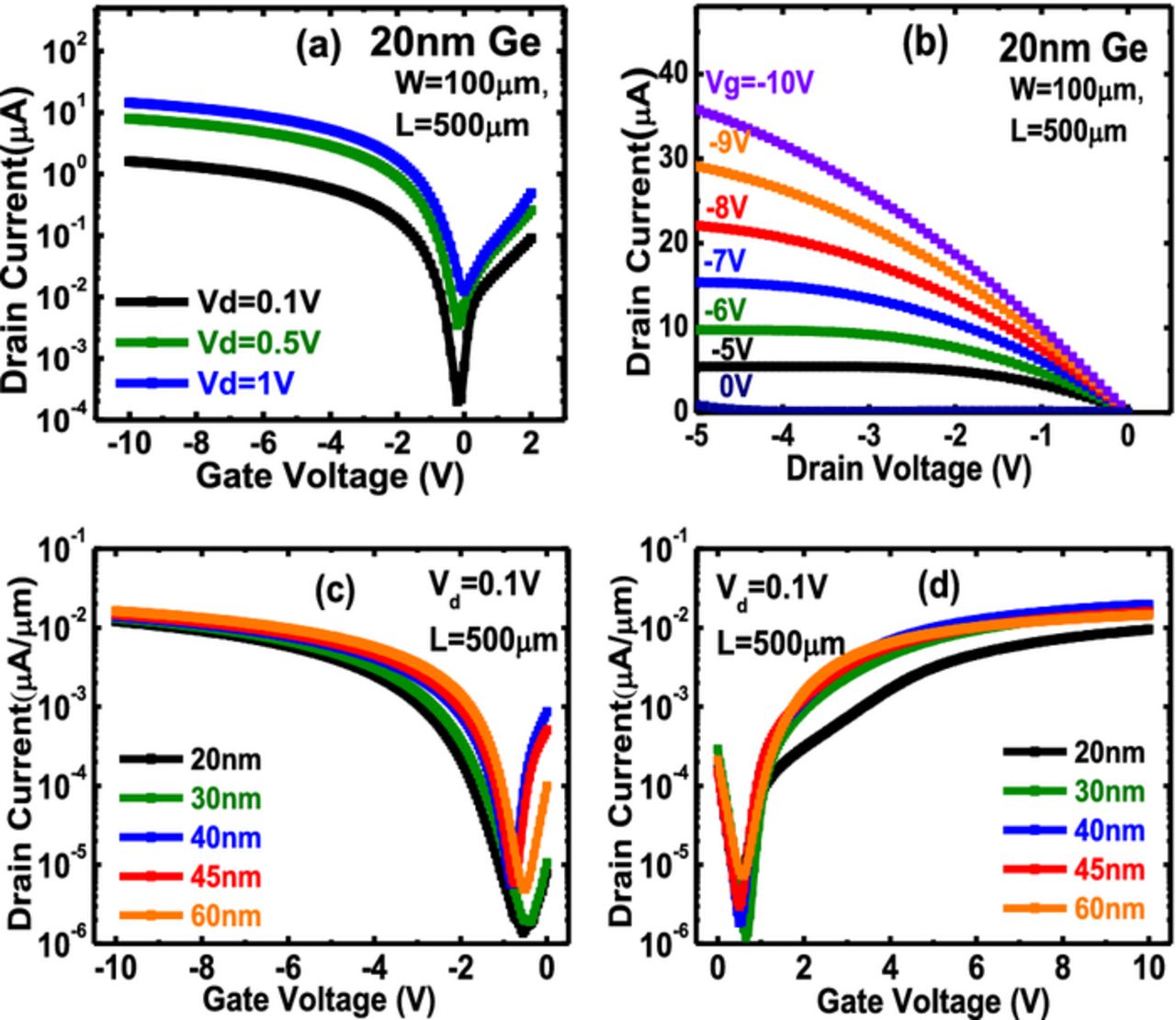
Figure 2. Id-Vg (a) and Id-Vd (b) curves of 20 nm pMOSFETs in inversion state. (c)Id-Vg curves of p- and (d)n-MOSFETs in inversion and accumulation state, respectively, with different Ge thicknesses range from 20 nm to 60 nm.
Furthermore, the Ge film thickness dependence of the electrical characteristics and the effective mobility of p- and n-MOSFETs were examined. The Id-Vg curves of p- and n-MOSFETs with the different GeOI thickness ranging from 20 nm to 60 nm are shown in Figure 2c and 2d, respectively. When the GeOI thickness increases from 40 nm to 60 nm, ION decreases, as shown in Figure 2d, because of the increase in the S/D parasitic resistance in n-MOSFETs. The similar transfer characteristics are observed among the MOSFETs with the different GeOI thicknesses.
The effective mobility was evaluated from the Id-Vg characteristics by the following equation because of the elimination of the parasitic resistance,

Here, the BOX capacitance Cox is derived from C-V curves (data not shown). Lm and Vm represent the channel length and the voltage, respectively, applied between the Hall bar terminals for excluding the influence of the S/D parasitic resistance by applying the 4-point measurement. The GeOI thickness dependence of the effective hole and electron mobility of inversion and accumulation mode GeOI MOSFETs is shown in Figure 3a and 3b, respectively. The peak hole mobility for the 20-nm-thick-GeOI MOSFETs is 122 cm2/Vs with substrate impurity concentration of around 2 × 1017 cm−3. This mobility value is 20% higher than that of a GeOI p-MOSFET based on Smart Cut GeOI wafers with 1ower than 2 × 1014 cm−3 doping concentration and the same Ge layer thickness,14 which is also shown in Figure 3a. The higher hole mobility in low field of the present 20-nm-thick-GeOI MOSFETs than that of the Smart Cut GeOI MOSFETs could be explained by a decrease of Coulomb scattering due to MOS interface charges at the Ge/BOX interfaces, which could be induced by the better interfacial properties of the Ge/GeOx interface introduced by plasma post oxidation than those of the Ge/SiO2 interface in the commercial GeOI. In addition, the mobility of the present device is higher than the universal Si p-MOSFET mobility at room temperature in ND = 2.7 × 1017 cm−3.21
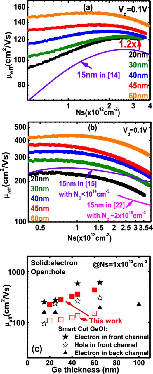
Also, the peak electron mobility is 235 cm2/Vs, comparable to that of the Smart Cut GeOI n-MOSFETs with a much lower doping concentration,13 as shown in Figure 3b. The thickness dependence of the hole and electron mobility in the same Ns of 1 × 1012 cm−2 of the present GeOI devices and the reported devices on Smart Cut GeOI are shown in Figure 3c. The degradation of the mobility of the present devices with a reduction of the GeOI thickness is not too severe, compared with that of the reported GeOI MOSFETs.12 This weaker mobility degradation with thinning GeOI thickness for the present devices might be attributable to the better MOS interface quality with BOX by using the GeOx/Ge interface, which is evident in the high mobility in bulk Ge MOSFETs with the same interface.9,10 The comparison between the mobility of present devices and the back channel mobility of the Smart Cut devices (Ge/SiO2 interface)14 is also shown in Figure 3c. The higher mobility of the present devices suggests that the Ge/BOX interface properties have been improved by the Ge/GeOx interfaces formed by the present method. Because the amount of the surface roughness was similar in the GeOI thickness range of 20∼60 nm, the mobility component limited by surface roughness could not vary in this GeOI thickness range. This fact would imply that the mobility degradation with thinning GeOI could not be attributed to surface roughness scattering. Judging from the mobility values, the peak mobility could be dominated by Coulumb scattering due to MOS interface charges and/or charges in the gate insulators. This is because the n-type substrate impurities in the present devices can be estimated to be ∼1017 cm−3 order.
In summary, we have demonstrated a novel method to fabricate GeOI substrates based on epitaxial Ge films grown on III-V compounds wafers. The plasma post oxidation process was introduced to improve the Ge/BOX back interface. By using the fabricated GeOI structures, p- and n-MOSFETs with the GeOI thickness down to 20 nm was fabricated and the electrical characteristics were evaluated. The normal p- and n-MOSFETs operations on the thin body GeOI structures have been confirmed in the inversion mode and the accumulation mode, respectively. The peak effective hole and electron mobility of 122 and 235 cm2/Vs, respectively, have been obtained. Furthermore, the GeOI film thickness dependence of the electrical characteristics and effective mobility has been systematically investigated. The mobility of the present devices higher than that of the Smart Cut devices with Ge/SiO2 interfaces is attributable to the better back interfacial properties by the GeOx/Ge interfacial layers. As a result, the GeOI substrates based on epitaxial Ge layers grown on III-V compounds wafers, combined with the BOX interfaces including GeOx interfacial layers, is promising techniques to realize high performance ultrathin body GeOI MOSFETs.
Acknowledgment
This work was partly supported by New Energy and Industrial Technology Development Organization (NEDO) in “Photonics Electronics Convergence Technology for Power-Reducing Jisso System” and Grant-in-Aid for Specially promoted Research from MEXT.