Abstract
Wafer geometry and residual stress go through significant changes at different points in the semiconductor manufacturing process flow. Precise wafer geometry measurement is very important to assess process induced wafer geometry change (PIWGC) and minimize pattern overlay in lithography steps of advanced node devices and 3-D (3-dimensional) packaged devices. However, the precise wafer geometry measurement is very difficult due to gravitational wafer sag and interaction between the anisotropy of mechanical properties of Si and wafer supporting configurations. Effects of anisotropy and supporting configuration on 300 mm Si (001) wafer profile measurements were investigated for pattern overlay estimation and process optimization.
Export citation and abstract BibTeX RIS

This is an open access article distributed under the terms of the Creative Commons Attribution 4.0 License (CC BY, http://creativecommons.org/licenses/by/4.0/), which permits unrestricted reuse of the work in any medium, provided the original work is properly cited.
Wafer geometry and residual stress go through significant changes at different points in the semiconductor manufacturing process flow.1–3 Wafer geometry, such as shape, flatness, bow, warpage, site flatness, nanotopography and roughness play a role in the execution of semiconductor manufacturing processes. As the device dimensions are shrinking and 3-D (3 dimensional) packaging is introduced, the precise wafer geometry measurement becomes very important.4,5 The monitoring and control of process induced wafer geometry change (PIWGC) is critical to achieving high device yield in advanced semiconductor manufacturing processes such as lithography, chemical mechanical polishing (CMP) and wafer bonding processes.3–12
Conventional wafer supporting methods (3- or 4-point supports) are less suitable for flatness characterization of large diameter wafers due to effects of gravity.4 Adverse effects of 3-point support methods and anisotropy on shape measurement accuracy was reported in detail.13,14 Gravitational wafer sag, for large diameter wafers with different thicknesses on different supporting structures as a function of wafer thickness, including 25 mm forks with various intervals and a front opening shipping box (FOSB) are significant issues.15 The weight of a 300 mm Si wafer, with a thickness of 775 μm, is 128 g and gravitational wafer sag is in excess of 100 μm at the center of wafer depending on how the wafer is supported. The self-weight deflection through finite element analysis (FEA) modeling of a 700 μm thick Si wafer supported by 3-point, 4-point and ring support is reported to be 206 μm, 160 μm and 130 μm, respectively.4 Epitaxial wafers with highly concentrated dopants such as boron (B) for p++ or phosphorous (P) for n++, can cause wafer warpage due to the alteration of the lattice constant by highly concentrated dopants.16 Gravity induced wafer deformation (or self weight induced deflection) of wafers will significantly differ in shape and magnitude depending on the supporting method during wafer surface profile measurements. Precise wafer surface profile measurement strategies and techniques need to be developed.
In this paper, effects of anisotropy and supporting configuration on 300 mm Si(001) wafer profile measurements was investigated for pattern overlay estimation and process optimization applications.
Figure 1 shows schematic illustrations of out-of-plane and in-plane distortion at different process steps and the effect of distortion on lithography steps.7 FEA simulation of chucking wafers with process induced wafer geometry change (PIWGC) showed clear correlation between the area of high curvature and residual wafer-chuck gap. The results demonstrated that the control of high-order PIWGC features is crucial to reduce pattern overlays.
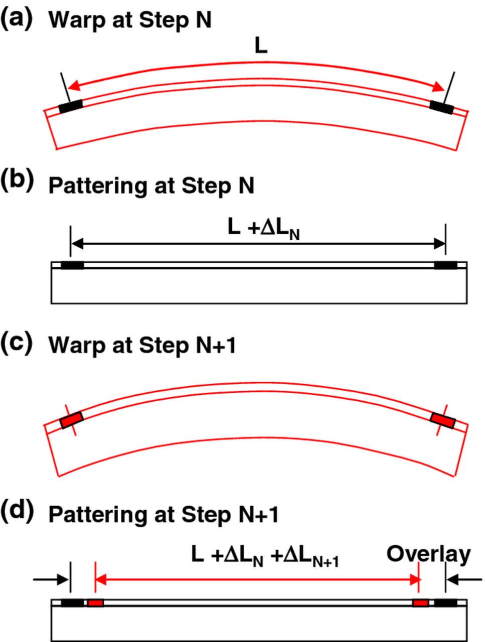
Figure 1. Schematic of out-of-plane and in-plane distortion at different process steps and their effect of distortion on lithography steps.7
Figure 2 illustrates the similar concept for bonded wafers. Device wafer bonding was done after pattern alignment at several places on the wafer.5,17,18 For wafer level 3-D approaches, more complex problems, (such as differences in profiles, device structures, device densities, residual stress, effective coefficients of thermal expansion (CTEs) of the two wafers) are associated. When foreign substrates are introduced, the problem gets even more complex.4 In 2-D lithography of mask-to-wafer alignment studies, misalignments are classified into three categories: translation (shift), rotation and run-out (expansion) misalignments.4 Translation and rotation errors are consistently minimized by continuous development and improvement of bond alignment tools. However, the run-out misalignment remains as one of the most challenging issues in wafer-level 3-D integration. Because the bonding and thinning processes cannot maintain the flatness of fully processed wafers in every layer-stacking process, fully processed wafers usually have different levels of compressive or tensile stress on the device layer.4 Temperature cycling during bonding or debonding processes changes stress, inducing wafer bow (warpage) and nonlinear distortion, which are the main cause of misalignments in bonded wafers. While a thick Si substrate maintains flatness despite stress effects, back side thinned wafers experience strong internal shear stress.4
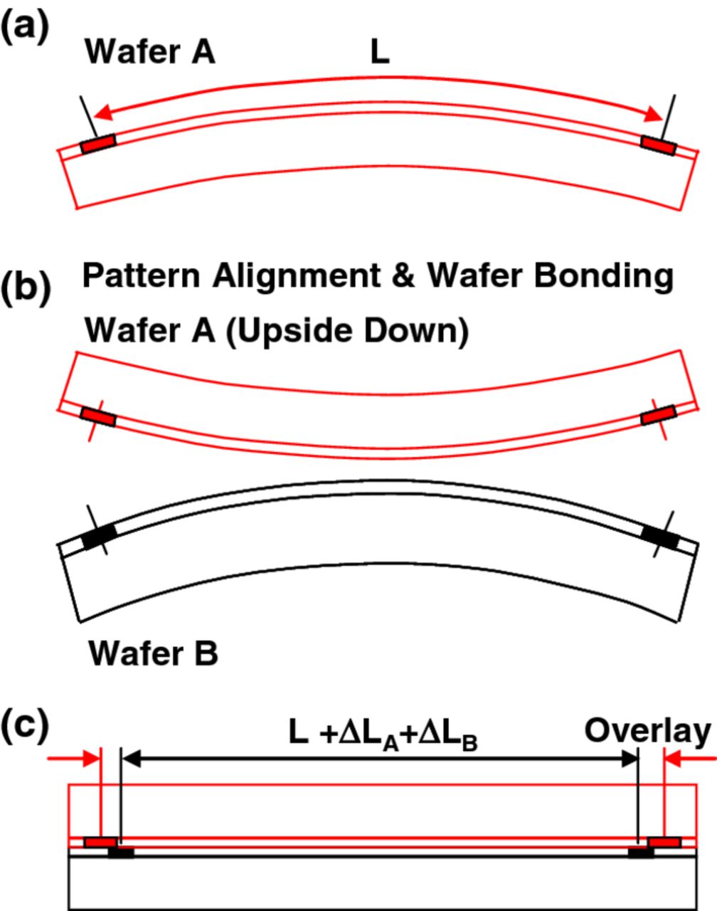
Figure 2. Schematic of out-of-plane and in-plane distortion at different process steps (before and after bonding).
New wafer-to-wafer alignment and bonding techniques are continuously being developed for high precision and accuracy.5,17,18 If no PIWGC exists, the pattern overlay problem would be a lot easier to understand and to address. PIWGC often distorts a 300 mm Si wafer to a convex or concave shape component. The warpage can sometimes exceed 100 μm. Warpage of 112 μm is equivalent to a radius of curvature of 100 m for a 300 mm wafer. It makes the 300 mm wafer diameter 112 μm smaller in diameter. The gravitational wafer sag and PIWGC are of the same order of magnitude. The gravitational wafer sag (warpage) and PIWGC can be considered as noise and signal. Since the signal-to-noise (S/N) is 1 or less, the gravitational wafer sag is no longer negligible.
For precise profile measurements, without significant gravitational wafer sag, a new wafer supporting method must be developed. Effects of anisotropy of a Si (001) wafer with respect to supporting methods on the gravitational wafer sag pattern and magnitude must be investigated. Figure 3 shows the angular dependence of Young's modulus and Poisson's ratio in Si (001) plane.19,20 Since the Si (001) plane has 4-fold symmetry, only one quadrant was illustrated. The notch of the Si (001) wafer indicates the [110] direction (45° direction in Fig. 3). Three other equivalent 〈110〉 directions appear in 90° intervals from the [110] direction. The four equivalent 〈100〉 directions are in the middle of two pairing 〈110〉 directions. Every 45° from the wafer notch, are equivalent 〈100〉 and 〈110〉 directions alternately. As seen in Fig. 3, Young's modulus and Poisson's ratio strongly depend on crystal orientation. Location and number of wafer supports will play a significant role in gravitational wafer sag and wafer surface measurement profile of Si (001) wafers, with or without PIWGC.
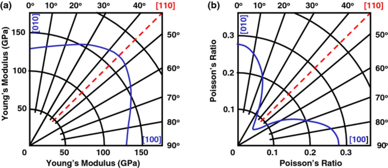
Figure 3. Angular dependence of Young's modulus and Poisson's Ratio in Si (001) plane.19
Surface profile of an ordinary Si (001) wafer was measured using a wafer surface profiler (WaferMasters OSP-3001,2) under various supporting methods (direct placement on a flat stage, two forks with a 236 mm interval, 3-pins 120° apart on wafer edge, 4-pins 90° apart on wafer edge, and ring-support). The wafer was also rotated from 0° to 360° in 15° intervals to see the effect of the wafer supporting method and crystal orientation with respect to supporting points.
The OSP-300 system irradiates a wafer with a laser beam at a fixed incident angle and captures optical (reflected, diffracted and scattered) images projected to the screen from the wafer (either blanket or patterned) to characterize the wafer surface profile and pattern distortions. The OSP-300 system can operate both radial scan and x-y scan modes.
The system detects the reflected and diffracted probing laser beam from the wafer surface using a two-dimensional (2-D) image sensor. The system can provide 2-D monitoring of global and local wafer shape (distortion and/or stress) of blanket and device wafers. The system generates wafer maps of vector plots, grid plots, intensity, height contours, distortion and 3-D surface profiles and shape-slope-residual (deviation from perfect parabola). PIWGC can be estimated and traced by comparing wafer surface profiles before and after a process step, or a series of process steps, for both blanket and patterned production wafers.
Figure 4 shows the effect of the wafer supporting method on wafer surface profile, deviation from ideal parabola, and grid plots, representing local distortion. Supporting method dependence was investigated in the following wafer support configurations: (a) on a flat stage, (b) on parallel rods with 236 mm interval perpendicular to 〈110〉 direction, (c) on the parallel rods perpendicular to 〈100〉 direction, (d) on 3-pins (one pin located at [110] direction), (e) on 3-pins (one pin located at [100] direction), (f) on 4-pins on 〈110〉 directions, (g) on 4-pins on 〈100〉 directions, and (h) on ring support.
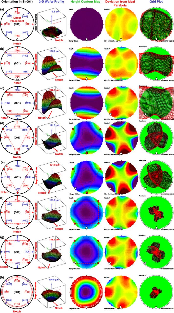
Figure 4. Effect of wafer supporting method on wafer surface profile, deviation from ideal parabola and grid plot representing local distortion. Supporting method dependence: (a) on flat stage, (b) on parallel rods perpendicular to 〈110〉 direction, (c) on parallel rods perpendicular to 〈100〉 direction, (d) on 3-pins (one pin located at [110] direction), (e) on 3-pins (one pin located at [100] direction), (f) on 4-pins on 〈110〉 directions, (g) on 4-pins on 〈100〉 directions, and (h) on ring-support.
Crystal orientation, wafer notch and supporting methods are illustrated in the far left column of the figure. The second and third columns from the left show 3-D wafer profiles in fixed vertical scales (0–250 μm) and 2-D height contour maps in absolute scales (0–250 μm), respectively. The warpage values were calculated and shown with the 3-D wafer maps. The fourth column shows the wafer map for deviation from ideal parabola (shape-slope-residual). The last column shows the grid plots. The perfectly flat wafer with no distortion should result in a square grid over the entire wafer. Wafers with perfect convex and concave profile should result in magnified grid pattern and shrunk grid pattern, respectively.
When a wafer was placed on a flat stage (Fig. 4a), the warpage was measured to be 9.2 μm due to the presence of local distortion. The local distortion, inherent to the wafer, can be seen from the figure. The same wafer was measured using different supporting method and notch orientation with respect to the support structures. When the wafer was placed on to two parallel rods with 236 mm interval, the warpage becomes very different depending on the wafer support directions. Wafer support in 〈110〉 directions (Fig. 4b) resulted in smaller gravitational sag of 177.8 μm compared to the gravitational sag of 242.1 μm for the wafer supported in 〈100〉 directions (Fig. 4c). This is direct observation of anisotropy of physical properties of Si. Under the same gravitational force, the 〈100〉 direction sags 36% more than the 〈110〉 directions. This is consistent with the difference in Young's modulus between the 〈100〉 and 〈110〉 directions.19,20
The most commonly used 3-point support showed smaller gravitational sag of 121.5 μm and 124.8 μm (Figs. 4d and 4e) compared to the sag for the two parallel rods (Figs. 4b and 4c). In one support configuration (Fig. 4d), one support pin was aligned with the wafer notch, the [110] direction. For the other configuration (Fig. 4e), the wafer was 45° rotated in clockwise directions to align one support pin with the [010] direction. Since a Si (001) wafer has 4-fold symmetry in-plane; there is no perfect match between 3-pins and crystalline geometry. Thus, the notch orientation dependence of gravitational sag should be smaller than for the two supporting rods case. All graphs show 3-fold symmetry representing pressure points at the 3-pins.
Figures 4f and 4g show gravitational wafer sag under 4-point support aligned with the four equivalent 〈100〉 directions and the equivalent 〈110〉 directions, respectively. With the increase of the number of support pins, the average gravitational stress on individual pins will significantly decrease. In fact, the 4-pin support in 〈100〉 direction and 〈110〉 direction resulted in 101.9 μm and 108.9 μm, respectively. Since the 4-pins align well with equivalent crystal orientations of 〈110〉 and 〈100〉 for a 45° rotation of the wafer, the higher support orientation dependence is expected, compared to 3-pin support cases. The angle dependent gravitational sag variation between 3-poins and 4-point supports was 3% and 7%. The 4-pin support showed higher support orientation dependence, as expected.
Figure 4h shows gravitational wafer sag on the ring-support. Relatively small wafer sag of 106.6 mm was measured. While the self-weight deflection through FEA modeling of a Si wafer supported by a ring showed very uniform and ideal parabolic wafer sag,4 three points were mainly contacted in our experiment. The contact points were determined by distortions inherent with the wafer. They were not equally spaced. Different points will be contacted on different wafers depending on the flatness of the individual wafers.
In 0–360° wafer rotation experiments in 15° steps, for 3-pin and 4-pin support configurations, 3-fold and 4-fold symmetry of gravitational sag patterns were measured. The average gravitational sag was higher for 3-pin supports than in 4-pin support, but angular dependence of 3-pin support was less than that of 4-pin support, similar to the results seen in Fig. 4d ∼ 4g. The gravitational wafer sag on the ring support (Fig. 4h) was relatively small, but the contact points cannot be controlled for repeatable measurement results. More than 5,000 measurements were performed using >100 wafers, with or without films, over the years. The repeatability of wafer profile measurements was experimentally confirmed.
Gravitational wafer sags in various supporting configurations and support orientations, with respect to crystal orientations, were investigated using the same wafer (300 mm diameter, prime Si (001)) in detail using the OSP-300 system. Effects of gravitational sag on wafer profile measurements should neither be ignored nor underestimated. In the case of rod, pin or ring support configurations, the number of pressure (contact or support) points and their location/orientation with respect to crystal orientation on Si (001) wafers can induce significant error in wafer profile measurement due to the significant gradational wafer sag compared to the PIWGC. Wafer placement on a flat surface would give better surface profile characterization results compared to conventional wafer supporting methods. During the lithography and wafer bonding process steps, wafers with PIWGC are placed on flat chucks to minimize the local distortion on the active wafer surface. Wafer profile measurements on a flat stage without vacuum or electrostatic clamping force, would make more sense than measuring wafer surface profiles under artificial wafer surface distortion from system design (balance between gravitational force and wafer support method/configuration). Anisotropy of physical properties of the Si (001) wafer plays a significant role in gravitational sag when the number of pins is small and all pins are aligned with primary crystal orientations of 〈110〉 and/or 〈100〉. For pattern overlay estimation and process optimization, placement of the 300 mm Si (001) wafer on a flat stage is strongly recommended to increase the S/N ratio by minimizing gravitational sag and to avoid introducing additional shear stress into the wafer due to gravity.