
Abstract
The electrodeposition of W was studied in detail using CsF–CsCl–WO3. Prior to electrodeposition, the WO3 solubility was confirmed to be 1.0 mol% at 773 K and increase with temperature. To investigate the effect of temperature on the crystal structure, electrodeposition was conducted at 6–25 mA cm−2 between 773 and 923 K with a unified charge density of 90 C cm−2. X-ray diffraction analysis confirmed that the crystal structures of the electrodeposited W films were β-W at 773 and 823 K, a mixed phase (α-W and β-W) at 873 K, and α-W at 923 K. The shape of the crystal grains varied with temperature: grains of β-W obtained at 773 and 823 K were spherical, while those of α-W obtained at 923 K were angular. Scanning electron microscopy observations showed that W films with smoother surfaces were obtained at lower current densities at all temperatures. In particular, a dense and smooth W film (surface roughness: 0.66 μm, thickness: 10 μm) was obtained at 6 mA cm−2 and 773 K. When the charge density was increased to 210 C cm−2 at 6 mA cm−2 and 773 K, a W film with a smooth surface and thickness of 30 μm was obtained.
Export citation and abstract BibTeX RIS

This is an open access article distributed under the terms of the Creative Commons Attribution Non-Commercial No Derivatives 4.0 License (CC BY-NC-ND, http://creativecommons.org/licenses/by-nc-nd/4.0/), which permits non-commercial reuse, distribution, and reproduction in any medium, provided the original work is not changed in any way and is properly cited. For permission for commercial reuse, please email: permissions@ioppublishing.org.
Tungsten (W) is a metal with superior properties, such as high heat resistance, high strength, and low thermal expansion, and is used in carbide tools, heat sinks, and nuclear fusion reactors. 1 However, owing to its hardness and brittleness, it is difficult to process tungsten into complex shapes and thin films. Therefore, a method for plating W on materials with good processability would significantly expand the range of applications.
Previous studies have shown that W films can be electrodeposited only from high-temperature molten salts. Oxides, 2–8 chlorides, 9–12 fluorides, 13,14 and chloride–fluoride mixtures 12,15–21 have been mainly used as molten salt electrolytes, and dense W films tend to be electrodeposited from oxide and fluoride melts. However, oxide melts have a relatively high operating temperature (over 1123 K), and fluoride melts containing insoluble salts in water make it difficult to remove them from the deposit.
Based on this background, we selected KF–KCl and CsF–CsCl for the electrodeposition of W films because they can be used at relatively low temperatures and consist of only water-soluble salts. 20,21 We previously reported the electrodeposition of α-W films in molten KF–KCl–WO3 at 923 K, and mixed-phase films of α-W and β-W in molten CsF–CsCl–WO3 at 873 K. 20 We also reported that β-W films with mirror-like surfaces were electrodeposited from molten CsF–CsCl–WO3 at 773 K. 21 These results suggest that temperature plays an important role in the crystal structure and grain growth, and thus in the surface smoothness, of electrodeposited W films. Therefore, in this study, we investigated the effect of temperature on the crystal structure and smoothness of W films electrodeposited from molten CsF–CsCl–WO3 at 773–923 K.
Experimental
Reagent grade CsF (>99.0%; Furuuchi Chemical Corp., Tokyo, Japan) and CsCl (>99.0%; FUJIFILM Wako Pure Chemical Corp., Osaka, Japan) were dried under vacuum at 453 K for more than 24 h and at 773 K for 24 h. The salts were mixed in a eutectic composition (CsF:CsCl with a molar ratio of 50:50, 150 g), and the mixture was loaded in a graphite crucible (o.d.: 55 mm and i.d.: 49 mm). The crucible was placed at the bottom of a stainless-steel vessel. Next, granular WO3 (1.0–8.0 mol%) (99.9%; Kojundo Chemical Laboratory Co., Ltd., Tokyo, Japan) was directly added to the melt as the W(VI) ion source.
The solubility of WO3 at 773–923 K was measured using the following method. An excess of WO3 was added to CsF–CsCl. Then, a small portion of the salts was sampled by the suction method using a borosilicate glass tube (o.d.: 6 mm, and i.d.: 4 mm) and dissolved in a HF–HNO3 aqueous solution (HF: 1 wt%, prepared from HF AA-100 grade, 38 wt%, Tama Chemical Co., Kawasaki, Japan; and HNO3: 10 wt%, prepared from HNO3, AA-100 grade, 68 wt%, Tama Chemical Co., Kawasaki, Japan). The solution was analyzed using inductively coupled plasma atomic emission spectroscopy (ICP-AES; SPECTROBLUE; Hitachi, Ltd., Tokyo, Japan).
For Raman spectroscopy, a small portion of the salts was loaded into a Pt pan (o.d. 5 mm × height 2.5 mm; Rigaku Corp., Akishima, Japan) before being transferred to an airtight high-temperature stage (10042, Japan High Tech Co., Ltd., Fukuoka, Japan). The high-temperature stage with the salt sample was then heated to 923 K under an Ar atmosphere. Raman spectra were measured with a micro-Raman spectrometer (Nanofinder 30, Tokyo Instruments Inc., Tokyo, Japan) using a laser source with an excitation wavelength of 532 nm.
Galvanostatic electrolysis was conducted in a dry Ar atmosphere using a three-electrode method with an electrochemical measurement system (HZ-7000, Hokuto Denko Corp., Tokyo, Japan). The working electrodes were Cu plates (99.9%, thicknesses: 0.03 and 0.05 mm, Nilaco Corp. Tokyo, Japan). A glass-like carbon rod (diameter: 3.0 mm; Tokai Carbon Co., Ltd., Tokyo, Japan) was used as the counter electrode. A Pt wire (99.98%, diameter: 1.0 mm, Nilaco Corp., Tokyo, Japan) was employed as the quasi-reference electrode. The melt temperature was measured using a type K thermocouple. To study the effect of temperature, the bath temperature was varied from 773 to 923 K. The effect of cathodic current density was also investigated by varying it in the range of 6.0 to 25.0 mA cm−2. The charge density was set at 90 C cm−2. In this study, all cathodic currents and charge densities were described as positive values. The electrolyzed samples on the Cu foils were soaked in distilled water for 10 min at 333 K to remove the salt that adhered to the deposits.
Phase identification of the samples was conducted using X-ray diffraction (XRD; Ultima IV, Cu-Kα, 40 kV, 40 mA; Rigaku Corp., Akishima, Japan). Scanning electron microscopy (SEM, Phenom Pro Generation 5, Thermo Fisher Scientific Inc., Waltham, MA) was used to analyze the sample surfaces and cross-sections, and measure the surface roughness (Sa). Before the SEM cross-sectional observations, the samples were embedded in acrylic resin, polished with emery paper and buffing compounds, and then coated with Au using an ion-sputtering apparatus (E-1010, Hitachi, Ltd., Tokyo, Japan) to impart conductivity. The crystallinity was evaluated using electron backscatter diffraction (EBSD, Supra 35VP- OIM6.2, ZEISS, Oberkochen, Germany).
Results and Discussion
Dissolution behavior of WO3
Prior to the electrodeposition of W, the dissolution behavior of WO3, including the solubility and structure of the W(VI) ions, was investigated. Table I shows the solubility of WO3 in CsF–CsCl at various temperatures, as determined by ICP-AES. The solubility at 773 K was found to be 1.0 mol%, and increased with temperature. Based on these results, a WO3 concentration of 1.0 mol% was used for the electrodeposition of W films to investigate the effects of temperature and current density.
Table I. Solubility of WO3 in molten CsF–CsCl at 773–923 K determined by ICP-AES after addition of excess WO3.
| Temperature/K | Added amount of WO3/mol% | Solubility of WO3/mol% |
|---|---|---|
| 773 | 2.0 | 1.0 |
| 823 | 2.0 | 1.4 |
| 873 | 8.0 | 3.1 |
| 923 | 8.0 | 4.9 |
In order to investigate the structure of the W(VI) ions in molten CsF–CsCl–WO3, Raman spectroscopy was conducted for molten CsF–CsCl–WO3 (2.0 mol%) at 923 K. The obtained Raman spectrum is shown in Fig. 1 together with the spectrum of molten KF–KCl–WO3 (2.0 mol%) at 923 K reported earlier. 20 Peaks were observed at 325, 315, and 920 cm−1, which are almost identical to those of KF–KCl–WO3. In our previous report, 20 the structure of the W(VI) ions in KF–KCl–WO3 at 923 K was determined to be fac-[WO3F3]3−, which has an octahedral structure with the W atom at the center, and the O and F atoms all located on opposite poles. 22 Therefore, the structure of the W(VI) ions in CsF–CsCl–WO3 was also confirmed to be fac-[WO3F3]3−.

Figure 1. Raman spectra of molten CsF–CsCl–WO3 (2.0 mol%) and molten KF–KCl–WO3 (2.0 mol%) [20] at 923 K.
Download figure:
Standard image High-resolution imageAnalysis of electrodeposited W films
Appearance and current efficiency
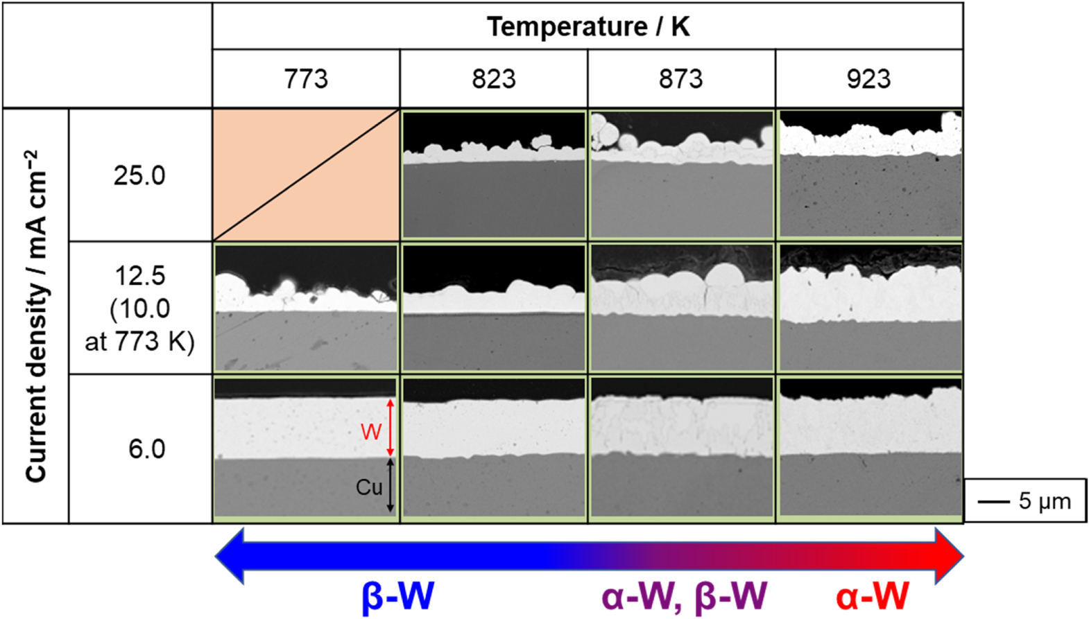
The appearance of the samples obtained by galvanostatic electrolysis at 6.0–25.0 mA cm−2 and 773–923 K in molten CsF–CsCl–WO3 (1.0 mol%) is shown in Fig. 2. At 773 K and 25.0 mA cm−2, no electrodeposit was obtained, most likely because the potential during electrodeposition was approximately 0 V vs Cs+/Cs, resulting in co-deposition with Cs metal fog. Gray- or silver-colored deposits were obtained under other conditions. At 773 K and 6.0 mA cm−2, a mirror-like surface was observed, suggesting high smoothness of the electrodeposited films. To calculate the current efficiency of electrodeposition, the mass change (mgain) was calculated by measuring the mass of the copper substrate before electrodeposition (mbef) and total mass after electrodeposition (maft). The current efficiency (η) was calculated assuming a six-electron reaction from W(VI) to W(0), using the following formula:

where F is the Faraday constant, S is the electrode area (1.015 cm2), q is the charge density (90 C cm−2), and MW is the molar weight of tungsten. The calculation results are presented in Table II. The current efficiency was as high as approximately 90% at 6.0 mA cm−2 and tended to decrease with increasing current density at all temperatures. One possible reason for this trend is that the concentration gradient of W(VI) ions near the electrode increased as the current density increased, and electrodeposition progressed preferentially in the convex area closer to the bulk bath, resulting in dendritic and granular deposition. Such deposits are easily detached during electrodeposition and/or washing, resulting in a lower current efficiency at higher current densities.
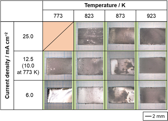
Figure 2. Optical images of the samples obtained by galvanostatic electrolysis of Cu plate electrodes at various current densities and temperatures in molten CsF–CsCl–WO3 (1.0 mol%). Charge density: 90 C cm−2.
Download figure:
Standard image High-resolution imageTable II. Current efficiency and surface roughness (Sa) in the electrodeposition of W on Cu plate electrodes at various current densities and temperatures in molten CsF–CsCl–WO3 (1.0 mol%).
| Temperature T/K | Current density i/mA cm−2 | Current efficiency a), b) η/% | Average roughness Sa/μm |
|---|---|---|---|
| 773 | 6.0 | 91.3 | 0.66 |
| 10.0 | 62.8 | 2.60 | |
| 25.0 | 2.1 | ― | |
| 823 | 6.0 | 76.2 | 1.85 |
| 12.5 | 68.3 | 2.28 | |
| 25.0 | 37.2 | 3.57 | |
| 873 | 6.0 | 85.1 | 2.27 |
| 12.5 | 82.0 | 2.72 | |
| 25.0 | 67.2 | 3.91 | |
| 923 | 6.0 | 90.3 | 2.30 |
| 12.5 | 89.3 | 1.73 | |
| 25.0 | 58.3 | 1.96 |
a): Calculated according to the 6-electron reaction for W deposition b):  M
w
= 183.84, S = 1.015 cm2, m
gain
= m
aft
− m
bef
.
M
w
= 183.84, S = 1.015 cm2, m
gain
= m
aft
− m
bef
.
XRD analysis
XRD patterns of the electrodeposits are shown in Fig. 3. The patterns of all the samples were attributed to metal W. However, the W phase varied with temperature; only β-W was detected below 823 K, both α-W and β-W at 873 K, and only α-W at 923 K. These results indicate that the crystal structure of the W electrodeposited from molten CsF–CsCl–WO3 depended on temperature. Moreover, as previously reported, 21 the W films electrodeposited at 773 K and 6.0 mA cm−2 were strongly oriented along the {111} plane.
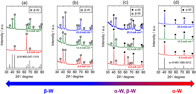
Figure 3. XRD patterns of the samples obtained by galvanostatic electrolysis of Cu plate electrodes at various current densities in molten CsF–CsCl–WO3 (1.0 mol%) at (a) 773 K, (b) 823 K, (c) 873 K and (d) 923 K. Charge density: 90 C cm−2.
Download figure:
Standard image High-resolution imageSEM observations
The surface morphology of the electrodeposited W was observed using SEM, and the results are shown in Fig. 4. The shape of the crystal grains varied with temperature; grains of β-W at 773 and 823 K were spherical, while those of α-W at 923 K were angular. At all temperatures, the W films appeared smoother at lower current densities. Furthermore, powder-like deposits were observed at higher current densities. To quantitatively investigate the smoothness of the deposits, the Sa was measured, and the results are summarized in Table II. The surface roughness measurements were carried out in a range: 401 × 401 μm (area) and 80 μm (cut-off length). At all temperatures, a smoother surface was observed at lower current densities. In our previous report, 21 the morphology change was explained by Fischer's classification of electrodeposition 23,24 as follows. Low current densities induce two-dimensional nucleation that forms a field-oriented texture (FT)-type deposit with a smooth surface. At relatively high current densities, three-dimensional nucleation, which forms the unoriented dispersion (UD) type, occurs, thereby forming a coherent deposit. A further increase in the current density enhanced the three-dimensional nucleation, resulting in the UD powder-type deposit. At a constant current density of 6.0 mA cm−2, a higher level of smoothness was obtained at lower temperatures. In particular, mirror-like W was obtained at 773 K and 6.0 mA cm−2. The Sa was 0.66 μm, indicating that the W was extremely smooth.
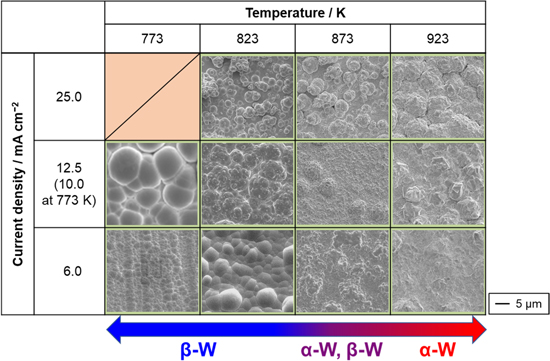
Figure 4. Surface SEM images of the samples obtained by galvanostatic electrolysis of Cu plate electrodes at various current densities and temperatures in molten CsF–CsCl–WO3 (1.0 mol%). Charge density: 90 C cm−2.
Download figure:
Standard image High-resolution imageThe cross-sectional SEM images of the samples are shown in Fig. 5. Consistent with the surface analysis results, lower current densities resulted in smoother surfaces. At 6.0 mA cm−2, the electrodeposited W films were dense and smooth. The film thickness was in the range of 8 to 10 μm.

Figure 5. Cross-sectional SEM images of the samples obtained by galvanostatic electrolysis of Cu plate electrodes at various current densities and temperatures in molten CsF–CsCl–WO3 (1.0 mol%). Charge density: 90 C cm−2.
Download figure:
Standard image High-resolution imageEffect of temperature on crystal structure
In the above results, β-W was obtained below 823 K, and a mixed phase of α-W and β-W was obtained at 873 K. Here, α-W is a stable phase with an A2 structure, while β-W is metastable with an A15 structure. 25 There have been several reports on the β-W formation mechanism. 10,25–28 In molten salt electrolysis, Hartmann et al. reported that β-W was obtained by galvanostatic electrolysis in a Na4P2O7–NaPO3–NaCl–WO3 melt at 873 K. 25 Takenishi and Katagiri investigated the effect of ZnO additives on W electrodeposition in a ZnCl2–NaCl–(K2WO4, WO3, WCl6, etc.) melt at 723 K. 10 They reported that β-W was deposited via the addition of ZnO. Shen and Mai obtained β-W by mixing oxygen in a sputtering chamber using physical vapor deposition (PVD). 26 The resulting β-W films were approximately 150 nm thick and contained 6–15 atom% O. Furthermore, Chattaraj et al. 27 and Sluiter 28 used ab initio molecular dynamics to simulate the β-W structure, and reported that β-W with a A15-type structure was thermodynamically more stable than α-W in a body-centered cubic lattice with the inclusion of O, N, and F.
From the above reports, it appears that oxygen plays an important role in the formation and stabilization of β-W. The amount of oxygen in W electrodeposited from CsCl–CsF–WO3 is probably higher at lower temperatures, resulting in β-W electrodeposition at lower temperatures. The reason for the inclusion of O in the electrodeposited W films may be that [WO3F3]3− is reduced while retaining its W–O bonds. The oxygen concentration in electrodeposited W should be further investigated in the future. Shen and Mai reported that β-W becomes unstable at high temperatures and changes to α-W under vacuum above 900 K. 26 This is consistent with the fact that no β-W was formed, and only α-W was obtained at 923 K, in this study.
Fabrication of thick W films
Since the smoothest W films with a thickness of 10 μm were obtained at 773 K, we attempted to electrodeposit thicker W films by increasing the charge density. Figure 6a shows the appearance of the electrodeposited W films obtained at 6.0 mA cm−2 and 210 C cm−2. The W films had a metallic luster and a mirror-like surface. The current efficiency was calculated to be 91.5%. The surface and cross-sectional SEM images are shown in Figs. 6b and 6c, respectively. The surface SEM images show that the films were smooth and composed of extremely small crystals. The thickness of the films was approximately 30 μm. No significant decrease in smoothness was observed with increasing thickness. The cracks near the substrate were most likely caused by tensile stress due to the difference in the thermal expansion coefficients between the Cu substrate and W film. These results indicate that W films can be electrodeposited at 773 K with both high smoothness and thickness. In previous studies, only thin films of nanoscale thickness have been reported for single-phase β-W formation by PVD. 26,29–34 Therefore, the fact that single-phase β-W with a film thickness of approximately 30 μm was obtained in this study is a significant advancement. Because β-W has a giant spin Hall effect, it has attracted considerable attention in the field of spintronics. 34,35 This electrodeposition method can be used to fabricate single-phase β-W with various thicknesses, ranging from thin to thick, which will have a significant impact on the spintronics field, including the elucidation of bulk physical properties.
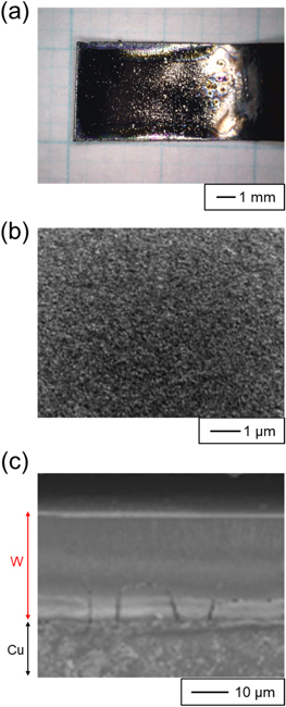
Figure 6. (a) Optical image, and (b) surface and (c) cross-sectional SEM images of the sample obtained by galvanostatic electrolysis of Cu plate electrodes in molten CsF–CsCl–WO3 (1.0 mol%) at 773 K. Current density: 6.0 mA cm−2. Charge density: 210 C cm−2.
Download figure:
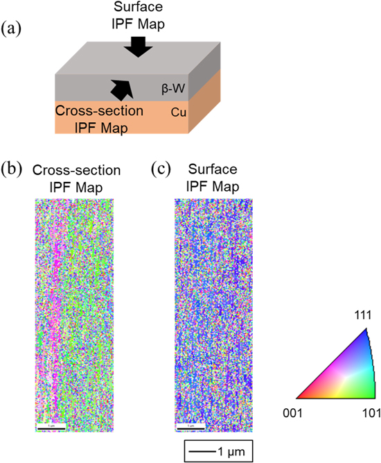
Standard image High-resolution imageEBSD analysis was conducted for detailed determination of the crystal orientation and grain size of the β-W thick film. The sample was prepared at 4.0 mA cm−2 and 210 C cm−2 at 773 K. The cross-section and surface were analyzed, as shown in Fig. 7a. Figure 7b shows an inverse pole figure (IPF) orientation map of the cross-section. There is no columnar crystal structure, and the grain size is very small (less than 100 nm). This result shows that grain growth during electrodeposition was significantly suppressed at 773 K. Figure 7c shows an IPF map of the surface. The crystal was strongly oriented along the {111} plane and almost uniformly distributed throughout the entire surface. This result is consistent with those of the XRD analyses of the W films obtained at lower current densities at 773 K.
Figure 7. EBSD maps for the sample obtained by galvanostatic electrolysis of Cu plate electrodes in molten CsF–CsCl–WO3 (1.0 mol%) at 773 K. Current density: 4.0 mA cm−2. Charge density: 210 C cm−2.
Download figure:
Standard image High-resolution image
Conclusions
The effect of temperature on the crystal structure of W films electrodeposited from molten CsF–CsCl–WO3 was investigated. ICP-AES analysis determined that the solubility of WO3 was 1.0 mol% at 773 K, and increased with increasing temperature. Raman spectroscopy revealed that the W complex-ion species in CsF–CsCl–WO3 was [WO3F3]3−, which was the same as that in KF–KCl–WO3. Electrodeposition was conducted at 6.0–25.0 mA cm−2 and 773–923 K. The structure of the electrodeposited W depended on the temperature (β-W at 773 and 823 K, mixed phase at 873 K, and α-W at 923 K). The surface of the W films became smoother at lower current densities and temperatures. Furthermore, at 773 K, the surface remained smooth even when the W film was thickened by increasing the charge density. EBSD analysis confirmed that the crystal size was small (less than 100 nm), indicating that grain growth was suppressed at 773 K. These results demonstrate that W films electrodeposited at 773 K exhibit both high smoothness and film thickness values.
Acknowledgments
Part of this study was conducted in collaboration with Sumitomo Electric Industries Ltd.