
Abstract
Cu electrodeposition in both underpotential and overpotential regimes on nanostructured MoS2 and WS2 prepared by plasma-enhanced atomic layer deposition has been studied in detail. A combination of electrochemical methods, advanced characterization by X-ray absorption spectroscopy (XAS) as well as theoretical modelling were employed to reveal Cu adsorption modes on transition metal dichalcogenides (TMDs) from initial stages until bulk deposition. Since Cu UPD on TMDs has been used recently to evaluate the number of electrochemically active sites (NAS) for H2 evolution reaction, we evaluate and discuss here the implications of the Cu electrodeposition phenomena on nanostructured MoS2 and WS2 gauging the general applicability of the Cu UPD method for number of HER active sites determination in TMDs. Although an apparently better correlation of HER current density with Cu UPD charge than with double layer capacitance is found, the Cu UPD method cannot be used quantitatively because of the absence of a clear H UPD phenomenon on the studied nanostructured TMDs. This is in contrast to platinum group metal catalysts where H UPD and Cu UPD sites are strongly correlated.
Export citation and abstract BibTeX RIS

This is an open access article distributed under the terms of the Creative Commons Attribution 4.0 License (CC BY, http://creativecommons.org/licenses/by/4.0/), which permits unrestricted reuse of the work in any medium, provided the original work is properly cited.
Underpotential deposition (UPD) refers to electrochemical deposition of metal atoms at potentials more positive than those required for bulk deposition.1 Typically, UPD is driven by the work function differences between two metals that a less noble metal is deposited on a more noble metal substrate at potentials above the reversible potential ( ). The adsorption and deposition of metal atoms in full or incomplete monolayers alter the structural, optical and electronic properties of the substrate profoundly. Thus, the UPD method has been broadly used for tuning activity and selectivity of catalysts, identifying of crystallographic facets, protecting catalysts from corrosion, determining trace metals, nanoparticle shape control, as well as surface area measurement determination.2–7 It is particularly convenient in determining the number of active sites (NAS) for noble metal electrodes or noble metal particles loaded on inert supports.8,9 For instance, Green et al. reported that both surface area and surface composition of Pt-Ru electrocatalyst could be determined by Cu UPD.8 Although precious metals such as Pt or Ru exhibit high activities for the hydrogen evolution reaction (HER), the scarcity and high cost of these elements have motivated the search for Earth-abundant metal-based catalysts with comparably high activities and stabilities. Recent advances in materials science and nanotechnology have demonstrated the significant potential of transition metal dichalcogenides (TMDs) such as MoS2 and WS2 as promising alternatives to Pt in catalyzing the HER.10 A variety of novel methodologies, e.g. nano-structuring and defect engineering, have been reported to fabricate TMD-based HER catalysts.11–13 However, comparison of experimental data from different laboratories or preparation methods is problematic without a proper normalization of the actual electrochemically active surface area (ECSA) or the number of active sites (NAS) of the different catalyst samples.1 Specific ex situ and in situ methods have been reported for different electrode materials, each with their own limitations.1 Correlations between the surface area determined by gas physisorption methods, such as the BET (Brunauer–Emmett–Teller) method, and the ECSA are typically poor.14 Hydrogen, oxygen, and CO adsorption are well known in situ electrochemical methods for determining NAS. Yet, these methods are limited in scope to only a few noble metals that show high affinity to these probe molecules. The electrochemical double layer capacitance (DLC), which is obtained from measurements in a potential region, where electric double layer charging is the only electrochemical process, offers a versatile alternative for estimating ECSA of compound electrocatalysts, such as sulfides, carbides and phosphides.12,15–17 However, a major challenge for this method is that it depends on the availability of a reliable value for the specific capacity per unit area.18–20 Furthermore, this method does not provide any information about NAS which is needed to determine the intrinsic activity of the catalyst under investigation.
Recently, UPD of Cu on metal chalcogenides (e.g. CdS, WS2, Pd3P2S8) has been reported and employed to access the number of electrochemically active sites.21–24 However, further studies are required to investigate the UPD adlayer formation and to correlate it with the actual nature and number of catalytically active sites. Therefore, we investigate here in detail the electrodeposition phenomena of Cu on nanostructured MoS2 and WS2 to get insight into the Cu adsorption modes and the transition between UDP and overpotential deposition (OPD) regimes by employing electrochemical and spectroscopic methods as well as theoretical modeling. Then, we evaluate the correlation between HER activity and Cu UPD to check how far the Cu UPD method is quantitative on TMDs towards NAS determination. Since, in contrast to Pt-group metals, no clear hydrogen UPD feature is present on the studied TMDs, we find it ambiguous to correlate the hydrogen adsorption sites with Cu UPD sites. Despite the apparent linear relationship between HER activity and Cu UPD charge, we indicate that Cu UPD cannot be generally employed as a quantitative method for determination of NAS on TMDs.
Experimental
Preparation of nanostructured TMDs
MoS2 and WS2 films were prepared by plasma-enhanced atomic layer deposition (PEALD) in an Oxford Instrument FlexALTM ALD reactor on either electrochemical quartz crystal microbalance (EQCM) gold electrodes or glassy carbon electrodes (Carbon-Vitreous-3000C-Foil-VC000550, Goodfellow Cambridge Ltd. UK).24,25 The PE-ALD process was based on a combination of a metal organic precursor bis(tert-butylimido) bis(dimethylamido) molybdenum ([(NtBu)2(NMe2)2Mo]) or [(NtBu)2(NMe2)2W] and H2S + Ar or H2S + H2 + Ar plasma as a co-reactant.24,25 WS2 and MoS2 films with different morphologies and number of ALD cycles, i.e. different thicknesses, are tested in this work.
Electrochemical characterization
Electrochemical characterization was performed in a three-electrode configuration cell with MoS2 or WS2 deposited glassy carbon plates (22 × 22 × 2 mm3) as the working electrode, Pt foil as the counter electrode (Pt contamination under the same conditions was excluded by XPS measurements in our previous research26) and a saturated calomel electrode (SCE, calibrated with a value of +0.269 V vs reversible hydrogen electrode (RHE)) as the reference electrode. Hydrogen evolution measurements were carried out in an Ar-saturated 0.1 M H2SO4 solution and Cu UPD was performed in an Ar-saturated 2 mM CuSO4 in 0.1 M H2SO4.
X-ray absorption spectroscopy (XAS)
XAS was performed at the 061D-1 (HXMA) beamline of the Canadian Light Source (CLS). Samples were mounted in an N2 protected holder and measured at a grazing incidence angle of 0.2° in fluorescence detection mode by using a 32 element Canberra array detector. X-ray Near Edge Spectroscopy (XANES) and Extended X-ray Absorption Fine Structure (EXAFS) spectroscopy were collected at the Cu K-edge (8.98 keV) and recorded by co-addition of 5 scans. The code used for XANES modeling was FDMNES.27 The structural model for metallic Cu was obtained from Crystallography Open Database (COD ID: 1512504).28 Structural models of Cu bonding on MoS2 were obtained from DFT calculations, which are discussed in detail in Part V of the SI.
Density functional theory (DFT) calculations
DFT calculations were carried out using the Vienna Ab-initio Simulation Package (VASP), a periodic plane wave DFT code which includes the interactions between the core and valence electrons via the Projector Augmented Wave (PAW) method.29–31 The generalized gradient approximation (GGA) with the Perdew–Burke–Ernzerhof (PBE) functional was used for the calculation of the electronic exchange-correlation potential.32 Wave functions were expanded in a plane wave basis with a high energy cutoff of 600 eV and the convergence criterion was set to 10−6 eV between two ionic steps for the self-consistency process. The long-range Van der Waals interactions were incorporated in the DFT calculations through the DFT-D3 scheme by Grimme, which adds a semi-empirical dispersion potential to the conventional Kohn–Sham DFT energy.33
Results and Discussions
Cu UPD on TMDs
Figure 1 displays the potential dynamic profiles of different MoS2 films during Cu UPD and overpotential deposition (OPD). For comparison, cyclic voltammetry (CV) curves of both the bare glassy carbon (GC) substrate and MoS2 film are given in Fig. 1a. From these data, we can conclude that the cathodic reduction of Cu2+ on MoS2 starts at more positive potentials than bulk Cu deposition on bare GC. The Nernst potential of  in this system (2 mM CuSO4) is +0.26 V vs RHE while the UPD on MoS2 shifts around +100 mV. A series of cyclic voltammograms with varying potential scan ranges were recorded (Fig. 1b). The data in Fig. 1 show the transition from Cu UPD to OPD with decreasing deposition potential. The complex loop between 0 and 0.2 V vs RHE as shown in Fig. 1b might be due to intercalation of Cu, which is reported in previous work.34,35 The same phenomenon is also observed for WS2 (Fig. 1d). Thus, Cu can be deposited on MoS2 and WS2 at potentials more positive than the Nernstian potential, or in other words Cu UPD occurs on MoS2 and WS2.
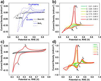
Figure 1. (a) Cyclic voltammetry (CV) curves of bare glassy carbon substrate (black curves) and MoS2 on glassy carbon (blue curves) in 2 mM CuSO4 in 0.1 M H2SO4 with different potential range 0.0–0.86 V vs RHE, scan rate: 50 mV s−1; (b) CV curves of nanostructured MoS2 in 2 mM CuSO4 in 0.1 M H2SO4 with gradually increased potential scan range; (c) CV curves of MoS2 on glassy carbon in 0.1 M H2SO4 (black curve) and 2 mM CuSO4 in 0.1 M H2SO4 (red curve), scan rate: 50 mV s−1; (d) CV curves of WS2 film in 2 mM CuSO4 in 0.1 M H2SO4 with potential range 0.0–0.86 V vs RHE. Scan rate: 50 mV s−1.
Download figure:
Standard image High-resolution imageElectrochemical quartz crystal microbalance (EQCM) measurements
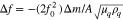
To study the UPD phenomenon of Cu atoms on MoS2 surfaces in more detail, we employed electrochemical quartz crystal microbalance (EQCM) measurements to quantitatively analyze the mass change during the Cu UPD process.36 Figure 2 presents cyclic voltammograms (CV) and the simultaneously recorded frequency change (Δf) on PE-ALD prepared MoS2-Au-EQCM electrodes in 2 mM CuSO4 in 0.1 M H2SO4. Upon negative scanning from +0.85 V, the QCM frequency first remains constant and then decreases quickly as the first Cu UPD peak appears at ∼+0.40 V. On the reverse scan, the frequency gradually increases accordingly when the Cu stripping peak approaches ∼+0.50 V. Although there might be drifts in EQCM, the Cu UPD and stripping peaks increase gradually within the first four CV scans and remain similar for the 5th and 6th scan, which is also reflected in the frequency change in EQCM measurements. In addition, the starting frequency (∼0.8 V vs RHE) value becomes larger with increasing scan numbers and remains constant after the 4th scan. This phenomenon can be ascribed to the strong binding between Cu atoms and MoS2 leading to an incomplete desorption of adsorbed Cu in the initial cycles. However, the absolute frequency change in each cycle (Fig. 2b) remains constant, which suggests that the same amount of Cu has adsorbed. The frequency change (Δf) in EQCM is proportional to the change in mass (Δm) per unit area (A) on the working electrode, given by the Sauerbrey equation:
where  is the resonance frequency (Hz), A is the piezo-electrically active crystal area,
  is the shear modulus of quartz (
 ) and
) and  is the density of quartz (
 ).36–39 Based on this equation, the sensitivity of the EQCM is calibrated to be
  Therefore, the adsorbed Cu atoms on the MoS2 electrode amount to
  or
or  in the range of +0.31 to +0.85 V vs RHE. Figure 2c, d displays the current density and corresponding frequency change at Cu UPD potential (0.44 V vs RHE) for 100 s. Given the 2-electron process for Cu UPD, the charge calculated via EQCM is 78 ∼ μC cm−2, which is higher than that obtained by integrating the current density over time (45 ∼ μC cm−2). The Cu UPD charge discrepancy between EQCM and recorded current density can be ascribed to the poor conductivity and hydrophobic effects of semiconducting MoS2 that result in significant deviations of Δf, which greatly lower the sensitivity of EQCM measurements.40 In conjunction with electrochemical measurements, XAS measurements were also performed to enable the assignment of structural configurations for Cu deposition on TMDs.
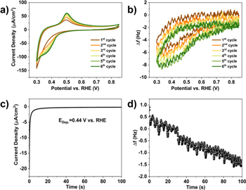
Figure 2. Cyclic voltammetry (CV) (a) and simultaneously recorded frequency change (b) on MoS2 deposited on a polycrystalline Au-EQCM electrode (400 ALD cycles, OoPo structure, Table SIII) in 2 mM CuSO4 in 0.1 M H2SO4. Scan rate: 50 mV s−1. (c) Current density curve (c) of Cu UPD at 0.44 V vs RHE for 100 s and the corresponding frequency change (d).
Download figure:
Standard image High-resolution imageXAS analysis
Grazing incidence X-ray absorption spectroscopy (XAS) at the Cu K-edge, including X-ray absorption near-edge structure (XANES) and extended X-ray absorption fine structure (EXAFS), allows for the investigation of the local structural environment and the site occupancy of adsorbed Cu on TMDs.41,42 As shown in Fig. 3, the similarity in the line shape between the sample of Cu deposition at 0.21 V vs RHE and Cu foil for the XANES edge jump within region "A" suggests that likely there is a Cu species with Cu-Cu direct bonding present in the measured sample. In addition, the clearly resolved edge shift by ∼2 eV (region "B" indicated by the arrow, Fig. 3a) indicates that there exists a second, different Cu species without Cu-Cu direct bonding, which may correspond to Cu atoms directly adsorbed on MoS2. The theoretically modeled Cu adsorbate system reveals a particle-size induced progressive change in the XANES features (Fig. 3b) for metallic Cu. The smallest particle used for the modeling is a cluster R3.0 Å (cluster size 3.0 Å), containing 12 Cu atoms. Figure 3c compares the sample spectrum and the XANES theoretical modeling based on a R3.0 Å cluster. The similarity in XANES between the two extends from the edge jump up to the white line (A1). In addition, the metallic Cu specific shoulder feature "C" is revealed for the measured sample and the theoretical model at around the same energy position, further suggesting a Cu-Cu direct bonding. Nevertheless, the edge shift in Fig. 3a is also well pronounced comparing with R3.0 Å, confirming the presence of Cu adsorption on MoS2. Thus, although the Cu deposition potential (0.21 V vs RHE) is slightly negative than UPD condition, XANES based observation suggests two coexisting Cu species in the sample, i.e., metallic Cu–Cu direct bonding, and Cu atoms adsorbed on MoS2.

Figure 3. (a) XANES spectra for Cu_MoS2@0.21 V (black curve) and Cu foil (red curve), label "A" indicates the spectral region in the rectangular box and label "B" indicates the spectra shift; (b) theoretical model of XANES system revealed particle size induced progressive changing in XANES features for metallic Cu, and the smallest particle used for the modeling possessed a cluster size of 3.0 Å (R3) containing 12 Cu; (c) XANES spectra of Cu_MoS2@0.21 V and R3, region "A1" represents the spectra in the rectangular region and label "C" indicates the shoulder feature.
Download figure:
Standard image High-resolution imageUsing density functional theory (DFT) calculations, we evaluated possible Cu bonding scenarios on MoS2, namely single Cu monodentate (M1, Fig. 4a), single Cu bidentate (M2, Fig. 4b) and paired Cu monodentate (M3, Fig. 4c) configurations. Fig. 4c presents the comparison of experimental and FEFF (automated program for ab initio multiple scattering calculations of XAS) modeled EXAFS magnitudes of Fourier Transforms (FT), which indicates the existence of M2 and M3 species upon Cu deposition at +0.21 V on MoS2, with bond distances of 2.36 Å for Cu-S (M2) and 2.56 Å for Cu–Cu (M3) (Table SIV is available online at stacks.iop.org/JES/167/116517/mmedia).27 As the Cu–K edge XAS was recorded for a sample with Cu deposition at a relatively negative potential (<+0.26 V vs RHE), it is reasonable to assume the existence of Cu-Cu direct bonding, indicating the presence of Cu-Cu, which is consistent with XANES analysis shown in Fig. 3. Although the sample was characterized under more negative potentials than Cu UPD, the strong contribution of the Cu bidentate (M2) configuration in the R-space of the Fourier Transformed EXAFS (Figs. 4d, 4e) indicates the bonding mode of Cu UPD on MoS2, which is also indicated by the edge shift in XANES (Fig. 3). It should be noted that the current EXAFS fitting models are based on Cu adsorption on MoS2 basal planes. Even though edge sites of TMDs have been identified to be the HER active sites, FEFF modelled XANES of adsorbed Cu on MoS2 edges (Fig. S16) did not fit well with the experimental data.43 However, DFT derived optimized structures of Cu on S–Mo–S edges (Fig. S15) indicates that Cu-bridge-S, which is structurally similar to bidentate binuclear M2 (Fig. 4b), has the largest (negative) average binding energy (Eab), which points to the adsorption of Cu atoms on edge or defect sites.44 Owing to the ultrathin, sub-monolayer nature of the Cu UPD layers on the MoS2 and WS2 samples, the S/N ratio of the data recorded for Cu UPD sample (Cu_MoS2@0.44 V) did not allow us to unambiguously prove the absence of Cu–Cu direct bonding (Fig. S11). Despite that, we think it is meaningful to show that even under lower deposition potential, we still observe the dominant peak of Cu on S edges (Fig. 4). Based on these data, further operando XAS measurements would be needed to investigate Cu UPD on TMDs in more detail.26
Figure 4. Structural models of Cu bonding on MoS2 with configurations of Cu monodentate (a), bidentate binuclear (b) and paired Cu monodentate (c); (d) comparison of experimental (black curve) and FEFF modeled EXAFS magnitude of Fourier Transforms (FT); (e) fitted results corresponding to the Cu K-edge EXAFS magnitude of FT spectra. Data are plotted as open circles and fits as red line.
Download figure:
Standard image High-resolution imageCritical evaluation of Cu UPD to determine NAS of TMDs
Recently, the Cu UPD method has been used to measure the number of HER active sites on WS2, MoS2 and Pd3P2S8.22–24 However, whether Cu adsorbs on the same sites, where hydrogen evolution happens, remains an unresolved question. Particularly as shown in Fig. 1, there is no clear H UPD region in MoS2 and WS2 making it impossible to derive QH. Nevertheless, the Cu UPD charge (QCu) and hydrogen adsorption charge ("QH") were compared and adopted in TMDs-based electrocatalysts.22–24 Here, we use the background capacitive charge (QBC) as a background correction to determine the charge which goes to the Cu UPD process (QCu). To correlate the relative QCu with QBC, a plot of QCu/QBC as a function of deposition potential is presented in Fig. 5a.8 QCu is obtained by integrating the Cu stripping charge from the Cu deposition potential (EDep.) to +0.67 V vs RHE (corrected for MoS2 background QBC in 0.1 M H2SO4), whereas QBC is calculated with the same method in the absence of CuSO4. The QCu/QBC ratio reaches a value of ∼2 in a narrow potential window of +0.44–0.46 V vs RHE for MoS2 (Fig. 5a, Table SI) and WS2 (Fig. 5b, Table SII). However, we should point out that QCu/QBC ratio of ∼2 does not necessarily suggest the same surface density between copper and hydrogen atoms under such conditions.22,23 First of all, the absence of a clear H UPD signature in MoS2 and WS2 leads to a unknown quantitative relation between Cu UPD and H UPD sites making a quantitative evaluation of H adsorption sites via the Cu UPD method impossible. Secondly, other factors such as (i) different accessibility of solvated Cu2+ to nanostructured TMD sites compared to H+, (ii) Cu cluster formation due to the improper selection of the Edep. window and scan rate, (iii) variations in crystallinity of TMD leading to presence of different HER active sites, and (iv) difference in nature of HER and Cu UPD sites such as basal plane adsorption of Cu on TMDs, can also influence the validity of Cu UPD method and are difficult to control. All these above aspects imply that the direct transfer of the Cu UPD method from noble metal systems with a clear H UPD phenomenon to TMDs appears to be not appropriate.

Figure 5. (a) Ratio of Cu stripping charge to background charge as a function of adsorption potential on nanostructured MoS2 in 2 mM CuSO4 in 0.1 M H2SO4. Inset shows the Cu stripping process where MoS2 is first polarized at +0.67 V vs RHE for 120 s, then after Cu deposition at certain potential EDep. for 100 s, the Cu is stripped by scanning back to +0.67 V at a scan rate of 2 mV s−1. (b) ratio of Cu stripping charge to background hydrogen adsorption charge as a function of adsorption potentials on WS2 film. (c)–(f) Plots of current density values of a selection of MoS2 (c), (d) an WS2 (e), (f) samples at −0.40 V and −0.60 V vs RHE vs double layer capacitance (Cdl) (black) and Cu stripping charge (QCu) (red).
Download figure:
Standard image High-resolution image
In order to further evaluate the applicability of the Cu UPD method in relatively comparing different samples based on the number of active sites for the electrocatalytic HER, we measured QCu, the double layer capacitance (Cdl) and the HER current density at −0.4 and −0.6 V vs RHE for a selection of MoS2 (Figs. 5c, 5d) and WS2 (Figs. 5e, 5f) samples; see Table SIII for sample IDs and preparation details. The linear sweep voltammetry (LSV) curves of different WS2 and MoS2 films are presented in Fig. S2, S6 and the current density values at certain overpotentials presented in Fig. 5 reflect their HER performance. QCu is calculated by integrating the CV curve of the samples in 2 mM CuSO4 in 0.1 M H2SO4 from +0.46 to +0.67 V vs RHE corrected for the background charge. The double layer capacitance (Cdl) was extracted by plotting Δj = ja − jc (ja and jc represent anodic and cathodic current densities, respectively) at a given potential against CV scan rates using the following equation:  (Fig. S3). Current densities at both −0.40 and −0.60 V show that WS2-5 presents the highest current density value. However, Cdl measurements show a significantly higher value for WS2-1 compared to the other WS2 films which clearly does not correlate with their HER activities. Therefore, evaluating the ECSA with Cdl in this case would lead to a random correlation with HER activity.19,45 In contrast, QCu values shown in Fig. 5e, f display the same trend as HER activity at both −0.40 and −0.60 V vs RHE, which suggests that Cu UPD apparently better correlates with HER activity and therefore would be a more reliable method for the determination of ECSA than Cdl. The correlation of Cu UPD (QCu) with HER activity of MoS2 films is shown in Figs. 5c, 5d. With Cu UPD we can assess the number of Cu UPD adsorption sites which apparently relates linearly to the HER activity of the tested samples allowing a relative comparison of NAS (Tables I, II). A quantitative relation between NCu UPD sites and NAS (HER) cannot be easily established due to the absence of the H UPD phenomenon on the tested nanostructured TMD samples. Further experiments, e.g. in situ scanning tunneling microscopy (STM) on single crystal MoS2 and WS2 model samples, would be needed to create a more solid link between NCu UPD sites and NAS (HER). Importantly, parameters such as deposition potential window and porosity of the catalysts should be considered when using Cu UPD as a method for ECSA estimation. With that, the relation between NCu UPD sites and NAS (HER) can be presented as NAS (HER) = a * NCu UPD + b with a being a constant between 0 and 1and b being a constant considering the Cu deposition on basal planes of TMDs and/or Cu cluster formation.
Table I. Summary of calculated adsorbed Cu based on the integration of Cu stripping in the range of 0.46–0.67 V vs RHE shown in Fig. S5.
| Sample name | NAS (amount of adsorbed Cu) cm−2 |
|---|---|
| WS2-1 | 2.8 × 10¹⁵ |
| WS2-2 | 1.1 × 10¹⁵ |
| WS2-3 | 2.5 × 10¹⁵ |
| WS2-4 | 7.7 × 10¹⁴ |
| WS2-5 | 5.9 × 10¹⁵ |
| WS2-6 | 1.8 × 10¹⁵ |
Table II. Summary of calculated adsorbed Cu based on the integration of Cu stripping in the range of 0.46–0.67 V vs RHE shown in Fig. S9.
| Sample name | NAS (amount of adsorbed Cu) cm−2 |
|---|---|
| MoS2-1 | 1.2 × 10¹⁴ |
| MoS2-2 | 2.2 × 10¹⁴ |
| MoS2-3 | 2.4 × 10¹⁴ |
| MoS2-4 | 4.4 × 10¹⁵ |
Conclusions
Underpotential deposition of copper on MoS2 and WS2 is investigated. EQCM has been used to show the adsorption of Cu atoms on TMDs under underpotential deposition conditions. The bonding structure of adsorbed Cu on MoS2 has been characterized by ex situ grazing incidence XAS in comparison with DFT models, showing a bidentate binuclear bonding on MoS2 basal planes. Compared to double layer capacitance measurements, Cu UPD demonstrates a better apparent correlation with HER activity and therefore would allow a more reliable evaluation of the number of HER active sites in TMDs. However, the formation of Cu clusters cannot be avoided with regard to a more negative (compared to Nernst Cu deposition potential) deposition potential range. Furthermore, due to the absence of H UPD, the correlation between Cu deposition sites—where basal plane adsorption cannot be excluded—and HER active sites (edge sites) needs to be further validated via in situ electrochemical STEM or XAS. Due to the complexity of the TMDs and the specific nature of their HER active sites (i.e. edge sites), a direct comparison with the Cu UPD phenomenon on noble metals such as Pt is not possible. A quantitative ECSA determination in TMDs requires edge site selective probes, such as used in NO titration FTIR spectroscopy as applied in our previous work.46
Acknowledgments
This work is part of the program "CO2-neutral fuels" (project 13-CO26) of the Foundation for Fundamental Research on Matter (FOM), which was financially supported by the Netherlands Organization for Scientific Research (NWO). This research program was co-financed by Shell Global Solutions International B.V. N.Y. Dzade acknowledges the UK Engineering and Physical Sciences Research Council (EPSRC) for funding (grant No. EP/S001395/1). This work also made use of the facilities of ARCHER (http://archer.ac.uk), the UK's national supercomputing service via the membership of the UK's HEC Materials Chemistry Consortium, which is funded by EPSRC (EP/L000202). S. Balasubramanyam, A. Sharma and A. Bol acknowledge financial support from the European Research Council (grant Agreement No.648787-ALDof2DTMDs).