

Abstract
Straight nanowires fabricated from single-layer porous anodic alumina (PAA) templates are known to be mechanically weak. To provide additional support, nanowires can be fabricated on multilayered PAA templates. In this work, Cu and Ni nanowires were fabricated using single-, double-, and three-layer PAA templates by pulse electrochemical deposition (PECD). The templates were made by anodizing Al-1 wt% Si and Al-0.5 wt% Cu thin films under different conditions. The morphologies of the PAA templates and fabricated nanowires were examined with scanning electron microscopy. The length of the nanowires was 3 μm, while the diameters ranged from 50 to 70 nm. The nanowires fabricated from a double-layered template (Al-0.5 wt% Cu/Al-1 wt% Si) were mechanically stronger with larger surface areas than those fabricated from an anodized Al-1 wt% Si template. The nanowires formed within the anodized Al-1 wt% Si layer had tree-like branches, while vertical nanowires with horizontal anchors were formed in the anodized Al-0.5 wt% Cu layer. The results also indicated that the volume expansion of the PAA template was controlled by depositing a Al-0.5 wt% Cu layer below the Al-1 wt% Si film. The Ni nanowires can be used as a platform for hydrogen production and in other technological applications.
Export citation and abstract BibTeX RIS
Porous anodic alumina (PAA) is a commonly used template for fabricating various nanostructures with a large surface area for use as components in sensors, filters, solar cells, and other devices.1 For decades, the anodic oxidation of Al-based surfaces in acidic (low pH) electrolytes has been used to produce oxide layers featuring high-density cylindrical nanopores or PAA. Compared to other molds such as polycarbonate membranes, PAA templates have smaller pore diameters, resulting in a higher pore density and the possibility of subsequently producing miniaturized devices.2 In practice, anodization is used to enhance the durability and appearance of Al-based modern consumer electronic products.
During anodization, the pore dimensions and PAA layer thickness can be controlled by modulating the anodization voltage, rate and time, and electrolyte concentration.3–6 Anodizing highly pure Al substrates under optimum voltage, electrolyte, and temperature conditions has been shown to produce PAA with regular and straight pores.7,8 However, branched pores are obtained when using a below-optimum anodizing voltage or Al-containing Si particles or impurities.9,10 Using an oscillating anodizing voltage or current on pure Al followed by chemical etching or anodizing Al-containing second phases produces PAA with interconnected pores (3D).11–14 In addition, many other PAA templates of multiple sizes, shapes, and morphologies can be obtained using different methods.15–18 The formation of 3D PAA from an impure Al substrate has been extensively studied, and the formation mechanism is well established.13,14 Recently, Zankowski and Vereecken fabricated interconnected Ni nanowires based on 3D PAA templates from Cu-doped Al substrates.19,20
The electrochemical deposition of materials inside the PAA mold requires a conducting layer at the bottom of the pores because the porous alumina bottom is an insulating layer that requires the presence of conductive seeds. This conducting layer can consist of the remaining Al layer below the anodized part or other conducting materials such as TiN. The conducting layer film is deposited prior to the post-anodization process. Hence, selective etching of the barrier layer is necessary prior to the growth of the nanowires inside the pores.
Metallic nanowires such as those formed from Ni and Cu have attracted considerable attention because of their interesting electronic and physical properties that allow for various technological applications such as energy storage and water condensation. Although there are a few published studies on the fabrication of these materials using a PAA template,16–32 the fabrication of multilayered nanowires from Cu and Ni elements has not been reported. However, the fabrication and characterization of Ni nanowires using a single anodized layer of Al-0.5 wt% Cu or Al-1 wt% Si as a template have been demonstrated.14,19–32
Although the process for forming PAA templates by anodizing Al-based materials using a single and homogenous concentration has been established, there is little information on fabrication of PAA based on the anodization of multi-layered Al with varying elemental compositions and morphologies.30 In this study, we modified the PAA template to combine two or three layers that have different morphologies, such as a combination of branched and interconnected pores, in separate layers on a single template. In addition, the prepared PAA templates were used for electroplating Cu or Ni to form a standard nanowire array combined with a 3D nanowire/lattice. The electrochemical responses during the anodization and electrochemical deposition processes were assessed and compared with previously published data. This combination of multiple layers of PAA with different morphologies can be used for various technological applications.
Experimental
The experimental approach consisted of fabricating the PAA template and metal (Ni, Cu) nanowires.
Fabrication of PAA templates
Three PAA template configurations were considered for this study. The first configuration was a single 2.6-μm-thick Al-0.5 wt% Cu layer (Fig. 1a), and the second configuration had 2 layers of 500 nm Al-0.5 wt% Cu deposited on 2 μm Al-1 wt% Si (Fig. 1b). The third configuration consisted of 500 nm Al-0.5 wt% Cu deposited on 2 μm Al-1 wt% Si, which was also deposited on 500 nm Al-0.5 wt% Cu (Fig. 1c). For each configuration, the thin layers were deposited using the sputtering technique on a 200 mm H-terminated (100) p-type silicon wafers (ρ ∼ 20 Ω cm) covered with 100-nm-thick TiN, as reported previously.3,6,7,12–14,33 The TiN layer was sputtered using the ionization metallization plasma technique. The thin films were anodized either in 1 M sulfuric acid (H2SO4) at a constant voltage of 20 V or 0.3 M oxalic acid (C2H2O4) at a constant voltage of 60 V. The anodization and electrochemical characterization of the samples were performed at a controlled room temperature of 22 °C. The anodization was conducted using a two-electrode setup where a Al thin film served as the working electrode (WE) and a Ti sheet served as the counter electrode (CE). The voltage was supplied by model PGSTAT100 potentiostat. The anodized surfaces of Al thin films had a circular area of 5 cm2. The PAA samples were rinsed with deionized water and dried in N2 gas immediately after anodization. The barrier layer was removed and the pores widened after chemical etching in 0.75 M phosphoric acid (H3PO4) at 22 °C and then in 49% hydrofluoric acid (HF) vapor (Pad Fume of Gemetec) at 35 °C.

Figure 1. Schematics of a (a) single-layer (Al-0.5 wt% Cu), (b) double-layer (Al-0.5 wt% Cu/Al-1 wt% Si) and (c) three-layer (Al-0.5 wt% Cu/Al-1 wt% Si/Al-0.5 wt% Cu) doped Al thin-films.
Download figure:
Standard image High-resolution imageFabrication of nickel and copper nanowires
In the present study, the PAA template was fabricated using a two-electrode setup, while nanowires were synthesized in a three-electrode system (working, counter, and reference electrodes). In all cases, Ag/AgCl/3 M NaCl (0.22 V vs SHE) was used as a reference electrode (RE), inert Pt gauze was used as a CE, and the WE was the anodized PAA templates. The CE was separated from the electrolyte with glass frit (GF) to avoid buildup of contaminants. The exposed surface of the WE had a circular area of 1.54 cm2. A sulfamate bath (0.01 M NiSO4.6 H2O, 0.05 M K2SO4, 0.1 M H3BO3) was used for the Ni deposition, while 0.3 M of CuSO4.5H2O with 40 g H₃BO₃ was used for the Cu nanowire deposition. To obtain free-standing nanowires or a nanolattice, the 3D PAA templates were etched in 3 M NaOH solution at 22 °C. The morphologies of anodized samples were examined using scanning electron microscopy (SEM, model, Philips XL30), while the pore parameters were calculated with ImageJ.34
Results and Discussion
Figure 2a shows the current density (i)-time (t) curves for the anodization of the Al-0.5 wt% Cu/Al-1 wt% Si/Al-0.5 wt% Cu films in 1 M H2SO4 at 20 V and 22 °C. The i-t transient curves depict the four different stages involved in the anodization process. The initial stage involved the formation of dense oxide followed by pore nucleation and organization. Then, the pore size reached a plateau at steady state before the Al substrate was finally consumed. Similar descriptions of the anodization mechanisms for Al samples have been previously reported.3,7,10,12–14,33,35 The time taken for Al to transform to PAA in 1 M H2SO4 was 31.8 min and 33.8 min for the Al-0.5 wt% Cu/Al-1 wt% Si (template 1) and Al-0.5 wt% Cu/Al-1 wt% Si/Al-0.5 wt% Cu (template 2) samples, respectively; based on these times, the anodization rates were 4.73 μm h−1 and 5.35 μm h−1, respectively. For samples anodized in H2SO4, the plateau current density was greater for anodized template 2 than for template 1. Accordingly, the anodization rate and duration were greater for template 2 than for template 1. This result was attributed to template 2 (∼3.0 μm) being thicker than template 1 (2.5 μm). Although the two top layers of Al-0.5 wt% Cu (500 nm) and Al-1 wt% Si (2 μm) were the same for the templates (Figs. 1b–1c), the plateau current densities for the early and middle stages of anodization differed. This difference may be attributed to the presence of the third layer of 500-nm-thick Al-0.5 wt% Cu deposited at the bottom of template 2. This layer is expected to influence the electrical properties and electrochemical behavior of the template during the anodization process.3 In addition, the higher current density (∼150%) in the plateau region for anodized template 2 compared to that for template 1 might have been caused by the higher concentration of Cu resulting from the presence of the bottom layer. This observation agrees with our previous work in which the anodizing of a single layer of Al-0.5 wt% Cu in 1 M H2SO4 at 20 V led to a higher plateau current than with the anodizing of a Al-1 wt% Si layer.33
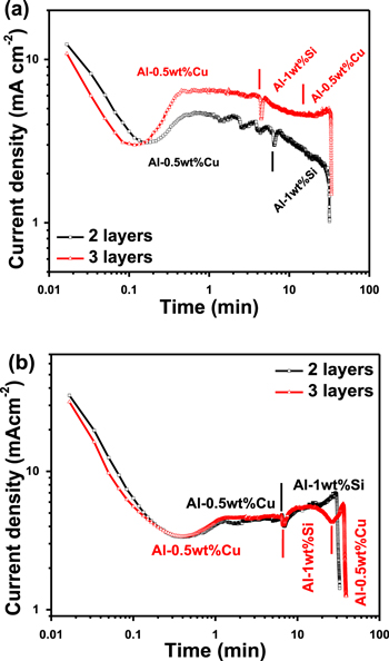
Figure 2. Current-time (i–t) transient curves during potentiostatic anodization of Al-0.5 wt% Cu/Al-1 wt% Si and Al-0.5 wt% Cu/Al-1 wt% Si/ Al-0.5 wt% Cu thin films using (a) 1 M H2SO4 at 20 V and (b) 0.3 M C2H2O4 at 60 V.
Download figure:
Standard image High-resolution imageFor samples anodized in 0.3 M C2H2O4, the transient curve differed from those for the anodization of a homogenous concentration of Al or single-layered Al films (Fig. 2b). Generally, the curve of current density vs anodization time for a single-layered Al thin films has four stages: a drastic decrease, gradual increase, plateau, and final decrease to zero or a minimum. Different behaviors were expected for templates 1 and 2. For example, the i-t curves had two and three distinct stages for the anodization of templates 1 and 2, respectively, compared to 4 stages for single-layered films. For template 1, the first stage was related to the anodization of the top Al-0.5 wt% Cu layer, while the second stage was attributed to the bottom Al-1 wt% Si layer. The current density drastically decreased, then gradually increased, reached a plateau, and then decreased to a minimum value. Surprisingly, the anodizing current density of bottom layer (Al-0.5 wt% Cu) of sample 2 in 0.3 M H2C2O4 showed only a plateau stage followed by a decrease to a minimum value. The absence of the first two stages indicated that the pore nucleation in the bottom layer was retarded by the presence of Si particles present in the middle layer (Al-1 wt% Si), leading to pore branching and subsequently delayed vertical pore growth toward the bottom layer. The plateau current was ∼1 mA cm−2 higher in the case of Al-1 wt% Si because of the Joule heating effect.7,10,33,35 The oscillations observed in the steady-state region were attributed to the formation of horizontal connections.13,14,33 The current density increased when the anodization transitioned to the third layer (Al-0.5 wt% Cu) and then dropped significantly after the exposed Al was consumed. In addition, the disappearance of the expected oscillations in the steady-state region in the i-t curve during the anodization of the third layer (bottom Al-0.5 wt% Cu layer) could be due to the fact that the pores did not reach the third layer because of the pore branching in the second layer. The anodization durations for Al in 0.3 M H2C2O4 were 32.7 min and 39.1 min for templates 1 and 2, respectively. Moreover, the anodization duration and rate as well as current density were greater for the anodization performed in 1 M H2SO4.
Figure 3 shows SEM images of the PAA template formed by the anodization of Al-0.5 wt% Cu/Al-1 wt% Si thin films in 1 M H2SO4 at 20 V. The interface between the two layers can be observed, and vertical pores can be seen in both layers (Fig. 3a). The thickness of the Al-0.5 wt% Cu and Al-1 wt% Si layers expanded to 0.756 μm from 0.5 μm and to 2.48 μm from 2 μm, respectively. The smaller expansion of the Al-1 wt% Si layer compared to that of the anodized single layer can be explained by the compressive stress imposed by the top layer, and the expansion can be minimized by modulating the anodizing voltage.6,36,37 Figure 3b shows the surface morphology of the top layer. The average pore size, pore circularity, inter-pore distance, pore density, and porosity were 23.2 nm, 0.8, 37.7 nm, 2.37 × 10¹¹ pores cm−2, and 24.7%, respectively.
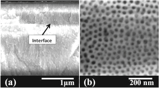
Figure 3. SEM images of (a) cross-section, and (b) top-view of Al-0.5 wt% Cu/Al-1 wt% Si layers anodized in 1 M H2SO4 at 20 V.
Download figure:
Standard image High-resolution imageFigure 4 shows the cross-sectional SEM images of the Al-0.5 wt% Cu/Al-1 wt% Si/Al-0.5 wt% Cu samples anodized in 0.3 M C2H2O4 at 60 V and 22 °C. The pore morphology differed from layer to layer. The top layer had vertical pores with horizontal interconnects, while the middle layer (Al-1 wt% Si) contained pores with a dendritic morphology. The bottom Al-0.5 wt% Cu layer had intricate tangled pores with horizontal interconnects. The thicknesses of the layers were 0.82, 3.2, and 0.59 μm for the top, middle, and bottom layers, respectively, after anodization with respective volume expansions of 1.64, 1.6, and 1.18. The unexpected change in the expansion of the Al-1 wt% Si layer shown in Fig. 3 or in Fig. 4 may be attributed to the electrolyte used and anodizing voltage applied.6 In this case, the expansion factor was 1.24 when the Al-1 wt% Si layer was anodized in 1 M H2SO4 at 20 V compared to 1.6 when anodized in 0.3 M C2H2O4 at 60 V. After the PAA templates were fabricated, the ∼60-nm-thick barrier oxide layer located below the pores was removed by etching in 5 vol% H3PO4 for 30 min at 22 °C. Then, the titanium dioxide formed from the oxidation of the TiN barrier layer was removed by etching with 49% HF vapor (Pad Fume of Gemetec) at 35 °C for 30 min.
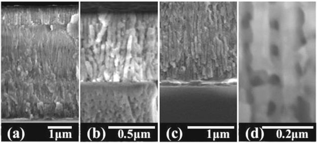
Figure 4. SEM images of a cross-section view of (a) PAA prepared by anodization of Al-0.5 wt% Cu/Al-1 wt% Si/ Al-0.5 wt% Cu in 0.3 M C2H2O4 at 60 V, (b) magnified top two layers, (c) magnified bottom layer, and (d) magnified top layer.
Download figure:
Standard image High-resolution imageThe electrochemical behavior of Ni deposited on a TiN-coated porous alumina substrate as assessed with cyclic voltammetry (CV) is depicted in Fig. 5a. The curve was recorded at a scan rate of 20 mV s−1 with Al-0.5 wt% Cu/Al-1 wt% Si PAA as the working electrode. Nickel reduction was featured at a potential of −0.78 V, whereas the hydrogen evolution was observed at a more negative potential of about −1 V (Fig. 5b). The anodic peak observed at a potential of −0.17 V can be attributed to the stripping of the electroplated Ni, and the area under the peak was proportional to the amount of electrodeposited nickel. Notably, the cathodic peak potential slightly shifted from Run-1 to Run-4 (Fig. 5b), and an increase in the rate of hydrogen evolution was also observed. The latter observation can be explained by the modification of the PAA electrode surface following the plate-stripping of Ni.38
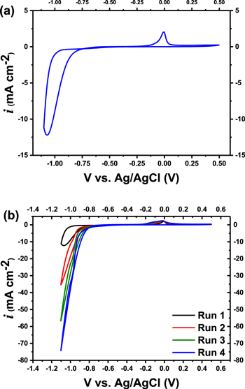
Figure 5. Cyclic voltammograms of ECD of Ni deposited in the anodized Al-0.5 wt% Cu/Al-1 wt% Si template (anodized in 0.3 M C2H2O4 at 60 V) at a scan rate of 20 mV s−1 performed in a sulfamate electrolyte for (a) single run, and (b) multi runs.
Download figure:
Standard image High-resolution imageFigure 6a shows the relationship between applied current density and electrodeposition duration for Ni or Cu metal deposited in PAA templates. The current, pulse time, and time delay (toff) were −25 mA cm−2, 10 ms, and 10 s, respectively. The process was repeated for two cycles while the applied current density was kept constant at −5 mA cm−2. As shown in Fig. 6a, the PECD occurred only during the first few seconds to obtain a homogeneous distribution of the Ni or Cu nanowires.32 Figures 6b and 6c show the response potential (U) as a function of electrochemical deposition time (t) of Ni inside the anodized Al-0.5 wt% Cu/Al-1 wt% Si (template 1) and Al-0.5 wt% Cu/Al-1 wt% Si/Al-0.5 wt% Cu (template 2) PAA templates, respectively. Ni metal started to be deposited in the pores of the PAA templates after application of negative current PECD. When a high current density was applied, high negative voltages of −1.5 (Fig. 6b) and −5 V (Fig. 6c) were obtained for the PECD of Ni anodized in templates 1 and 2, respectively. Then, a delay time of 10 ms allowed the recovery of the Ni2+ ion concentration at the deposition tips and limited the hydrogen evolution. This was followed by constant voltages around −0.97 V and −0.98 V for the deposition in anodized templates 1 and 2, respectively. The constant potential during the electrochemical plating reflected the phenomenon of Ni growth inside all the opened pores. However, potential changes were observed during the transition from layer to layer during electrochemical deposition (Figs. 6b and 6c). These changes may be due to the change in the exposed surface area. For example, in Fig. 6b, the potential changed from −0.97 V to −0.94 V as anodization transitioned from the Al-1 wt% Si layer to the Al-0.5 wt% Cu layer. These potentials indicate that the exposed area of Al-0.5 wt% Cu was greater than that of the Al-1 wt% Si layer, possibly because of the interconnection of the vertical pores in the first layer. PAA templates were then etched in 3 M NaOH after the PECD process to obtain free Ni or Cu nanowires. The templates were removed rapidly because of the high etching rate of alumina in NaOH.39

Figure 6. (a) Applied current density as a function of time for PECD process, and potential (U)-time response curve for anodized (b) Al-0.5 wt% Cu/Al-1 wt% Si template and (c) Al-0.5 wt% Cu/Al-1 wt% Si/ Al-0.5 wt% Cu template using 0.3 M C2H2O4 at 60 V.
Download figure:
Standard image High-resolution imageFigure 7 shows SEM images of the anodized Al-0.5 wt% Cu template (a, b) and the Cu nanowires (c–e) fabricated from it. The images clearly indicate that the nanowires were uniformly distributed with a size similar to the pore diameter of the template. In addition, the interconnects ensured that the horizontal nanowires provided mechanical strength for the vertical nanowires. The average length, diameter, and Cu nanowire area fraction were 3.25 μm, 76 nm, and 56.5%, respectively. The electrochemical transition during the Cu deposition in the PAA template (Fig. 7f) exhibited a similar behavior as that observed for Ni (Fig. 7g). A high negative voltage of −0.39 V was observed when a high current density was applied. This stage was followed by a constant voltage around −0.17 V. This nanowire architecture is similar to those previously reported,32 and their characteristic high surface area and mechanical stability make them attractive for use in applications such as nanoelectronics, optoelectronics, energy, and magnetic storage, biologic technology, and sensors.

Figure 7. SEM images show (a) cross-section view, and (b) top-view of anodized Al-0.5 wt% Cu at 60 V in 0.3 M C2H2O4 at 22 °C. The SEM images in (c), and (d) show top-view of the formed Cu nanowire after partially, and fully removing the PAA template, respectively, and (e) SEM image show a cross-section of Cu nanowire after removing the PAA template. (f) Applied current density as a function of time for the PECD process, and (g) potential (U)-time response curve for PECD of Cu nanowires inside the PAA template.
Download figure:
Standard image High-resolution imageFigure 8a shows a cross-sectional SEM image of the fabricated Ni nanowires before the Al-0.5 wt% Cu/Al-1 wt% Si template was removed. Clearly, Ni nanowires filled both layers, while freestanding nanowires were obtained after the PAA template was etched (Figs. 9b–9c). A 3D lattice was observed in the top layer (Fig. 8d). An interface between the layers was also seen, with some continuity between the nanowires above and below resembling inverted shrubs (Fig. 8c). It was also noted that the nanowires were more stable than the Ni nanowires fabricated from the anodized single layer of Al-1 wt% Si template.
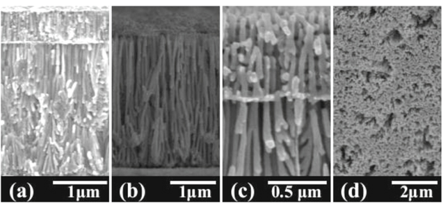
Figure 8. SEM images of (a) Ni nanowires prepared using anodized Al-0.5 wt% Cu/Al-1 wt% Si template, (b) cross-section view of Ni nanowires after removing the PAA template, (c) magnified of (b), and (d) the Ni nanowires through the top (Al-0.5 wt% Cu) layer after removing the PAA template.
Download figure:
Standard image High-resolution image
Figure 9. SEM images of (a) cross-section view of Ni nanowire array inside anodized Al-1 wt% Si layer, and (b) tilted view of the Ni nanowires after removing the PAA template using NaOH. SEM image of (c) top-view and (d) cross-section view of Ni nanowires after Al-0.5 wt% Cu/Al-1 wt% Si template was removed. In (c) and (d) images, the PECD plating process was terminated as the Ni plating reach the top (Al-0.5 wt% Cu) layer.
Download figure:
Standard image High-resolution image
Figure 9a shows a cross-sectional SEM image of Ni nanowires inside the PAA template fabricated using only the anodized Al-1 wt% Si layer.32 The nanowires were attached to the bottom substrate (TiN) and grew in one direction within the PAA. However, these nanowires collapsed because of their surface tension and magnetic attraction after the PAA template was removed, as shown in Fig. 9b. This drawback was solved with the multi-layered 3D template fabricated in this study.
The length of the fabricated nanowires can also be controlled by stopping the PECD of material at a designated time. For example, homogenous Ni nanowires of equal length were obtained when the deposition process was terminated after reaching the top layer (Al-0.5 wt% Cu) (Figs. 9c–9d). Although the Ni nanowires (Figs. 9a–9b and 9c–9d) were obtained using the same templates (Al-1 wt% Si template), the images shown in Figs. 9c–9d indicate non-collapsed nanowires with a homogenous distribution compared to the Ni nanowires shown in Figs. 9a–9b. Obviously, the presence of the top layer (Al-0.5 wt% Cu) in the Al-0.5 wt% Cu/Al-1 wt% Si template prevented the nanowires from collapsing during the removal of aluminum oxide and wetting process.
Conclusions
The anodization of single, Al-0.5 wt% Cu/Al-1 wt% Si and Al-0.5 wt% Cu/Al-1 wt% Si/Al-0.5 wt% Cu thin films was performed in H2SO4 and C2H2O4 to form PAA templates with different morphologies. Mechanically strong Ni and Cu nanowires were fabricated by PECD using these templates. The nanowires fabricated within the top layer of the template were vertical with horizontal connections, while those below resembled inverted shrubs. The diameters ranged from 50 to 70 nm and were mechanically stronger with a larger surface area than those fabricated from a single-layer template. The Ni nanowires can serve as a platform for hydrogen production, optoelectronics, energy and magnetic storage, biologic technologies, sensors, and other applications.
Acknowledgments
The authors would like to thank Prof. P.M. Vereecken (imec-Belgium) for his support of the experimental work while hosting at imec-Belgium. The authors would also like to thank Dr. Tesleem B. Asafa (Ladoke Akintola University of Technology, Ogbomoso, Oyo State, Nigeria) for his help.