
Abstract
In order to substitute traditional cyanide-based baths and obtain a new eco-compatible route to synthesize via electrodeposition a CZTS (copper-zinc-tin sulfide) absorber films, this paper describes the development of a green electrodeposition bath for Cu–Sn alloys. CZTS, being a p-type semiconducting material could be used in novel and sustainable photovoltaic devices. In this work we analyzed the electrochemical behavior of different methanesulfonic acid-based prototype deposition bath containing tin methanesulfonate as tin precursor, copper sulfate or methanesulfonate as copper precursor, and hydroquinone, nitrilotriacetic acid and 2-picolinic acid as organic additives. Electrodeposition was conducted with different deposition parameters such as deposition potential, current density, potentiostatic or galvanostatic mode. Surface and cross-section morphology as well as composition of the films were characterized using SEM-EDS. The composition of the samples in terms of crystalline phases was analyzed using XRD, highlighting the information obtained by superlattice diffraction peaks based on the crystallography of Cu–Sn intermetallic phases. From prototype bath S4 a uniform composition around Cu:Sn = 2:1 was observed with  phase as the dominant phase, which could possibly facilitate the synthesis of CZTS due to its aligned body-center vacancies that could serve as sulfur diffusion path during sulfurization within each
  crystal.
Export citation and abstract BibTeX RIS

This is an open access article distributed under the terms of the Creative Commons Attribution 4.0 License (CC BY, http://creativecommons.org/licenses/by/4.0/), which permits unrestricted reuse of the work in any medium, provided the original work is properly cited.
The solar photovoltaic (PV) market in recent times has steadily grown, achieving in 2014 a global operating capacity of 177 GW; this may play an important role in electricity generation in a few countries, but still does not contribute a sizeable fraction of the global energy needs, currently estimated at 17 TW-yr yr−11 Various reasons contribute to the limited adoption of PV technology. Silicon solar cells currently make-up ∼85% of the PV market2 but are still more expensive (per unit energy produced) than conventional energy sources. Thin-film chalcogenides present advantages over Si, as they feature a direct bandgap that results in a high absorption coefficient (α > 104 cm−1),3 and lower sensitivity to grain-boundary recombination, allowing the use of thinner and polycrystalline materials, thus decreasing raw materials and manufacturing costs. CdTe2 and chalcopyrite CuInGa(S,Se)24 based devices exhibit high efficiency (up to 22.9%),5 but recently have experienced limited growth, due to the fact that these technologies rely on relatively rare elements in the Earth's crust (In, Te),6 and/or to the toxicity of Cd, which is banned in some countries. An alternative material for PV absorbers made up of abundant elements only, stable in air, and with demonstrated > 10% efficiency7 are the compounds Cu2ZnSnS4/Cu2ZnSn(S, Se)4 (CZTS/CZTSSe)8.
While CZTS/CZTSSe crystallize in various structures, the thermodynamically stable one is the kesterite structure.9 Both CZTS and CZTSSe exhibit a direct bandgap of 1.4–1.5 eV, p-type doping (1015 to 1020 cm−3) controlled in part by stoichiometry,10 and most importantly the low sensitivity to grain boundary recombination. Despite these characteristics, CZTSSe which is more efficient than CZTS,11 has so far reached an efficiency of only 12.6%12 The inferior performance is usually ascribed to the complexity of this compound and the limited stability range of the chemical potential of the constituent elements. Various electrodeposition methods13 have been targeted a pure kesterite phase,14 including our efforts, which aimed for pure phases and ideal stoichiometry, also using a top electrode to avoid gravity effects.15,16 While the overall target of this project is the electrodeposition of Cu2ZnSn precursor films for a CZTS/CZTSSe absorber, in this paper we seek to develop a novel, low environmental impact electrodeposition bath capable to reliably form a smooth, dense Cu–Sn alloy with a 2Cu: 1Sn stoichiometry; clearly the alloy will not be single-phase, due to the lack of an intermetallic with this stoichiometry in the phase diagram.
This novel Bronze (Cu–Sn alloy) electrodeposition formulation avoids the use of cyanide as a complexing agent; this is in contrast with current industrial bronze deposition baths which include highly concentration cyanide (15–60 g l−1).17 Moreover, methanesulfonic acid (MSA) is used both as the electrolyte and complexing agent. MSA is a useful compound from various points of view18; it is biodegradable (undergoes the Sulfur natural cycle), it shows poor oxidizing behavior against metal ions and organic compounds and features a conductance comparable with that of commonly used acids, thus enabling a lower cell potential to reach a comparable current density.
Experimental
Electrodeposition of Cu–Sn alloys
Throughout the development of the various formulations, various additives and ion precursors have been investigated, with the aim to identify the best combination in terms of electrochemical performance and bath stability. The list of the reagents used for the proposed deposition baths and their abbreviations are listed in Table I. Note that the water utilized in all the experiments had a maximum conductance of 3 μS cm−1.
Table I. Reagents of the experiment.
| Reagent | Supplier | Purity grade | Abbreviation |
|---|---|---|---|
| Methanesulfonic acid | Sigma Aldrich | Reagent Plus ≥ 99% | MSA |
| Hydroquinone | Sigma Aldrich | Reagent Plus ≥ 99% | Hyd |
| Nitrilotriacetic Acid | Sigma Aldrich | Sigma Grade ≥ 99% | NTA |
| 2-Picolinic Acid | Sigma Aldrich | ≥ 99% | 2-Pic |
| Copper Sulfate heptahydrate | A.M.P.E.R.E. s.r.l | technical grade | Cu(II)SFT |
| Copper(II) Methanesulfonate | Todini & co. s.p.a. | Solution 125 g l−1, technical grade | Cu(II)MSA |
| Tin(II) Methanesulfonate | Todini & co. s.p.a. | Solution 300 g l−1, technical grade | Sn(II)MSA |
The films studied in this work were deposited on Cu–Zn(bulk)/Ni(∼20 μm)/Au(∼0.5 μm) substrates and from various electrolytes, as detailed in Table II. Deposition areas were controlled by immersion area of the substrates in the deposition baths.
Table II. Prototypes composition. The first column shows the formulation number and the composition of each formulation for each row.
| # | MSA | Hyd | NTA | 2-Pic | Cu(II) SFT | Cu(II) MSA | Sn(II) MSA | pH |
|---|---|---|---|---|---|---|---|---|
| 1 | 200 cc l−1 (3,08 M) | 10 g l−1 (0.09 M) | 20 g l−1 (0.105 M) | — | 11 g l−1 (0.17 M) | — | 11 g l−1 (0.09 M) | <1 |
| 2 | 200 cc l−1 (3,08 M) | 10 g l−1 (0.09 M) | — | 20 g l−1 (0.105 M) | 11 g l−1 (0.17 M) | — | 11 g l−1 (0.09 M) | <1 |
| 3 | 200 cc l−1 (3,08 M) | 10 g l−1 (0.09 M) | 20 g l−1 (0.105 M) | 1 g l−1 (0.01 M) | 11 g l−1 (0.17 M) | — | 11 g l−1 (0.09 M) | <1 |
| 4 | 200 cc l−1 (3,08 M) | 10 g l−1 (0.09 M) | 20 g l−1 (0.105 M) | 1 g l−1 (0.01 M) | — | 11 g l−1 (0.17 M) | 11 g l−1 (0.09 M) | <1 |
| 5 | 200 cc l−1 (3,08 M) | 10 g l−1 (0.09 M) | — | 20 g l−1 (0.105 M) | — | 11 g l−1 (0.17 M) | 11 g l−1 (0.09 M) | <1 |
| 6 | 200 cc l−1 (3,08 M) | 10 g l−1 (0.09 M) | 20 g l−1 (0.105 M) | 1 g l−1 (0.01 M) | — | 11 g l−1 (0.17 M) | 22 g l−1 (0.18 M) | <1 |
Voltammetric analyses were carried out in a three-electrode cell using a 3 × 0.5 cm2 polycrystalline Platinum plate working electrode and a 9 × 2 cm2 polycrystalline Platinum plate counter electrode. The tests were performed with a Metrohm Autolab mod. PGSTAT302N Potentiostat/Galvanostat computer-controlled by Nova® 2.1.4 software (Metrohm) using Ag∣AgCl (0.197 V vs SHE at 25 °C and KCl sat.) electrode as reference, with respect to which all potentials recorded in this study are referred. The potential range for cyclic voltammetry (CV) measurements started at −0.7/−0.8 V to +1.0 V and return, with a scan rate of 50 mV s−1.19 Samples grown under potentiostatic conditions were made using the PGSTAT302N applying a potential in the range from −0.25 V to −0.65 V. Samples obtained under galvanostatic conditions were grown using an ELC bench power supply mod. ALR3002M (voltage undulation < 3 mV peak to peak or 1 mV RMS and current undulation < 1 mA RMS20) ranging from 0.865 A dm−2 to 2.173 A dm−2 (corresponding to a current range from 0.039 A to 0.163 A). The range of potentials and consequently of current densities had been selected to cover a wide range of electrochemical conditions of metal deposition and study the evolution of the film composition and crystalline structure.
Materials characterization
The SEM images and alloy compositions were acquired from a FEI Quanta 650 with an Energy Dispersive Spectroscopy (EDS) attachment, with an acceleration voltage of 20 kV. The interaction of the 20 keV electron beam with Cu0.5Sn0.5 film was simulated using Casino v2.4821 with 50000 electrons. The thermodynamics of the Cu–Sn system was calculated by a custom-made Python program, with the energetic and entropic data extracted from references,22,23 while the crystallographic analyses were conducted using the CrystalMaker suite24,25 combined with the Inorganic Crystal Structure Database (ICSD)26 The X-ray Diffraction patterns were collected in the θ−2θ (Bragg-Brentano) configuration, using a PANalytical Empyrean X-ray diffractometer with Cu Kα as the source (dual-wavelength  = 0.1540 nm,
  = 0.1544 nm,
  ).
).
The cross-sectional views of the samples were prepared by gluing the deposit with Si wafer pieces as the protective counter by Crystalbond™ (Ted Pella, 821–3) at the temperature of 150 °C for 30 s. The samples were then mechanically clamped, followed by a conventional grinding-polishing recipe and setup, finished with 1 μm diamond paste. The Si support was removed mechanically at 150 °C within 30 s, while the residue Crystalbond was cleaned by immersing in acetone and methanol for 6 h each.
Preparation of prototype baths
Each bath prototype had been prepared adding the constituents in the presenting order in Table I from left to right, under stirring and at ambient temperature, except for the NTA, where the system had been warmed to 50 °C to accelerate its dissolution.
The solutions were prepared utilizing MSA as the supporting bath, resulting in all solutions having pH < 1. Prior to the study of the complete formulations, some preliminary tests were carried out to understand the physicochemical and electrochemical behavior of the constituents. During these tests it was observed that the dissolution of Nitrilotriacetic Acid in the water/MSA system gave an unstable solution as reported in the literature. However, under the presence of hydroquinone, NTA was dissolved and the solution was observed to be stable, which had never been reported to the best of our knowledge. The change in the solubilization behavior of NTA could be due to intermolecular weak interactions between NTA and Hydroquinone, which may facilitate the dissolution of the commonly water-insoluble Nitrilotriacetic acid.
Results
Cyclic voltammetry measurements
Cyclic voltammetry (CV) was used to qualitatively assess the redox potential peaks for each metal ion, while varying formulation with the aim to minimize the separation among the cathodic peaks. The CVs were carried out between − 0.7 V and 1 V. The initial metal precursor couple being studied were Cu(II)SFT and Sn(II)MSA. Two types of organic additives had been used in this first formulation: hydroquinone and nitrilotriacetic acid. Hyd acts as an anti-oxidant, helping to avoid tin precipitation as tin oxide or hydroxide.27
Hyd oxidizes to benzoquinone (Fig. 1), preventing the oxidation of Sn2+ to Sn4+, through the appropriation of the electrons derived from the oxygen solubilized in water. Its action could be easily explained by the simple redox reactions as follows:


NTA (Fig. 2) is a Copper chelating agent, which at acidic pH values forms univalent complexes and allows a two-monoelectronic-steps mechanism for the reduction of Cu2+ ions.28–30

Figure 1. Hydroquinone-benzoquinone couple.
Download figure:
Standard image High-resolution image
Figure 2. Nitrilotriacetic acid structure.
Download figure:
Standard image High-resolution imageThe two following reactions could explain the chelating behavior of NTA:


Using the above components, we formulated the prototype formulation # 1 (see Table I).
Figure 3 depicts the CV diagram due to the combined redox processes of Hyd, copper, and tin. The cathodic direction of the first scan (black line) shows two reduction peaks of copper with Vp,c = −0.28 V, a peak at −0.48 V (highlighted in the inset) due to two-monoelectronic-steps mechanism assigned to NTA, and the Tin reduction peak with Vp,c = −0.64 V. In the anodic direction the tin oxidation peaks at Vp,a = −0.46 V, copper oxidation occurs at Vp,a = +0.3 V, and a broad signal is shown due to the oxidation of Hyd to benzoquinone with Vp,a = +0.74 V. In the second scan a peak appears at Vp,c = 0.00 V, corresponding to the broad reduction of benzoquinone. From an electrochemical point of view this solution appears to be suitable to produce alloy samples, because the reduced separation between the second copper reduction peak (Vp,c = −0.48 V) and the tin reduction peak (Vp,c = −0.64 V) makes them overlap, obtaining a range of potentials in which the two elements could codeposit. Deposits from this bath prototype however have not been made, because within a few days this solution formed a white precipitate (probably Sn(OH)4), suggesting limited and unsuitable stability for our purposes.

Figure 3. Cyclic Voltammetry (50 mV s−1) of prototype # 1.
Download figure:
Standard image High-resolution imageIn order to improve the bath stability, we investigated a different complexing agent, 2-Picolinic Acid.
The two following reactions could explain the chelating behavior of 2-Pic:


2-Pic (Fig. 4) is another Copper chelating agent,31 which allows one dielectronic-step mechanism for the reduction of Cu2+ ions32 Two different electrolyte formulations utilizing this molecule have been produced (prototypes # 2 and # 3), allowing studies of bath stability and the behavior of Cu2+ ions. Bath prototype # 2 contained only 2-Pic, while prototype # 3 contained both NTA and 2-Pic.
Figure 4. 2-picolinic acid structure.
Download figure:
Standard image High-resolution imageAs can be seen in the CV of single metal precursor formulations (Figs. 5a and 5b), the addition of Hyd affects the electrochemical behavior of both metallic ions in solution, while NTA and 2-Pic interact only with Copper ions. Figure 5a (Sn(II)MSA solutions data) shows that Hyd reacts both as an Sn2+ complexing agent and as a hydrogen discharge inhibitor, while NTA and 2-Pic do not have an appreciable effect on Sn2+ electrochemical behavior. Figure 5b shows the activity of organic additives on Cu(II)SFT ions. As shown in the voltammograms, Hyd has a retarding effect both on the onset cathodic potential and the peak current potential of Cu2+ ions, but the addition of NTA and 2-Pic results in a greater shift on the cathodic peak potential of these ions.
Figure 5. Cyclic voltammetry comparison (50 mV s−1) of single metal precursor (5.a and 5.b) formulations vs protypes formulations # 2 (black line) and # 3 (red line) (5.c).
Download figure:
Standard image High-resolution imageFigure 5c compares the CV of the two alloy deposition baths. These results illustrate that the cooperation of NTA and 2-Pic causes a splitting of the copper reduction peak, suggesting a difference in the Cu reduction mechanisms due to different complexing agents. As can be deduced from Figs. 5a and 5b, NTA presents a similar effect to 2-Pic, affecting the redox potentials of both Cu2+ and Sn2+. Thus, the differences observed in the redox potential of metal species in the alloy deposition formulations (Fig. 5c) with respect to the single metal precursor formulations (Figs. 5a and 5b) are probably related to enthalpic interactions induced by alloying33 The use of two complexing agents also results in the improvement of bath stability.
Both solutions did show limited stability, so we tested an alternative combination of metal precursors to further improve stability. Specifically, we substituted the Cu(II)SFT precursor with Cu(II)MSA, thus formulating two additional prototypes. These two solutions are listed as # 4 and # 5, respectively, and their additive composition is comparable with that of prototypes # 2 and 3 (see Table I).
Figure 6 reports the comparison between the new single metal precursor formulations labeled as Fig. 6a and 6b and the new Cu and Sn precursors formulations (Fig. 6c) corresponding to prototypes # 4 and # 5). In the voltammograms in Fig. 6c the presence of two metallic ionic species in solution with different standard reduction potentials causes for the less noble element (Tin) a reduced area signal respect to the same cathodic signal in Fig. 6a (in Fig. 6c Vp,c, red = −0.56 V or Vp,c, black = −0,6 V) due to the limiting current of the more noble metal (copper), whose reduction peaks in Fig. 6c are Vp,c, red = −0.36 V and −0.24 V or Vp,c, black = −0.22 V. Comparing the CVs in Figs. 6a and 6b (i.e. the single metal formulations) to the CV in Fig. 6c (i.e. alloy deposition formulations) the onset potential of copper reduction is negatively shifted by 0.1 V in both the bath prototypes.
Figure 6. Cyclic voltammetry comparison (50 mV s−1) of single metal precursor formulations (6.a and 6.b) vs prototypes # 4 (red line) and # 5 (black line) (6.c).
Download figure:
Standard image High-resolution imageThe location of the reduction peaks suggest that Cu and Sn have been stabilized by each other, but this stabilization doesn't derive from the mechanism of the anomalous codeposition as in the case of Fe-Ni or Zn-Ni alloys,34 because in our case the nobler element is always present in greater quantity in the films deposited. During the electrodeposition from a solution of two different metal ions as in this case, there can be some interactions between the reduction processes of the single metal ions. These interactions can stabilize the ions and cause a mutual shift of the reduction potentials in the positive or in the negative direction. In the first case we talk about depolarization in the latter we talk about overpolarization. The causes of depolarization and overpolarization can concern thermodynamic factors, surface-adsorption factors and kinetic factors.
The characteristic effect of the cooperation of 2-Pic and NTA is the evident differentiation in the Cu2+ reduction mechanism, as already observed in Figs. 3 and 5c. The last prototype (# 6) has the same composition of prototype # 4 but with a doubled concentration of Sn(II)MSA, in order to obtain a 1:1 copper:tin molar ratio in the electrodeposited film, necessary in the attempt to synthesize Cu2ZnSnS4.
CV data of bath # 6 are compared to bath # 5 in Fig. 7; doubling the concentration of Tin precursor causes an increase of its cathodic and anodic peak area (red line, anodic peak current at −0.26 V and cathodic peak current at −0.57 V). Moreover, the CV results show a variation in the cathodic Cu+ traces: the reaction Cu+ → Cu0 (peak current at −0.38 V) is significantly increased with respect to the same peak obtained from the solution with a Cu:Sn precursor molar ratio equal to 1:0.5 (black line).

Figure 7. Cyclic voltammetry (50 mV s−1) of prototype # 5 (black line) compared with prototype # 6 (red line).
Download figure:
Standard image High-resolution imageOverall, the various additives introduced in the electrolyte do not significantly change the equilibrium potential of both Sn and Cu, suggesting that limited complexation occurs at pH below 1. However, NTA and 2-Pic are found to slow down the kinetics of Cu2+, while the Sn deposition rate is almost unaffected. Tentatively, we hypothesize that the local pH increase due to hydrogen evolution enables NTA and 2-Pic to dissociate and complex with Cu2+, thus slowing the kinetics of Cu reduction.
Thermodynamics and crystal structure of electrodeposited films
Due to the importance of Cu–Sn interfacial reactions in soldering processes, the phase diagram of Cu–Sn alloys has been studied extensively. Low-temperature annealing of the Cu–Sn diffusion couple yields the phases of  and
and  Moreover, even at room temperature, other intermetallic phases more stable than the disordered
  (fcc) phase can be formed, showing a strong affinity between Cu and Sn and their strong tendency for ordering. At high temperature around 15%Sn, at, the bcc solid solution phase β is more stable than the fcc solid solution phase α, suggesting the possibility of a stable bcc phase owed to the presence of Sn. Modeling of the binary Cu–Sn system has been investigated since 199635–40; different models revealed varying stability of β(bcc) at low temperature in the Sn-rich region, as shown in Fig. 8. The models considered suggest that metastable
  and
and  phases are very close to the stability line
  −
− indicating their small degree of metastability.
Figure 8. Free energy (G/RT) vs XCu curve for the Cu–Sn binary system at T = 298 K, extracted from various CALPHAD works.22,23
Download figure:
Standard image High-resolution imageCrystal structure of the phases present in the experimental Cu–Sn phase22,23 (including the  (hcp) phase in electrodeposited Cu–Sn)41–44 are summarized in Table III. The calculated XRD profiles of these phases have similar, strong reflections, making it difficult to identify such phases. We hypothesize that these intermetallic phases are somehow related to each other, therefore we use the software CrystalDiffract24 to fit the patterns to face-centered and body-centered structures by continuously varying their lattice parameters. Through this process, we categorize the intermetallic phases as different parent phases and fit their corresponding parent-phase lattice parameter, which is listed in columns 7–9 of Table III. For some phases, however, the choice for the bcc lattice is not unique; for example, each set of Miller indices {
 } and
} and  may represent the (001) planes of the bcc structure but could also be related by 2-fold rotation along (010) of
  Therefore, we assume that these bcc units are related to symmetry operations for the crystal through either 2-fold or 3-fold rotational axes as listed in Table III, which was visualized by reducing the symmetry of the crystal to P1 (consisting only of translations) before calculating their XRD profile in CrystalDiffract, such that the original degenerate planes with respect to the rotation axes could be reduced and all possible combination of the planes could be shown.
Table III. Crystal structure and relations of Cu–Sn phases appearing in the phase diagram (with one additional α'(hcp) phase came from Cu–Sn electrodeposition papers).
| Phase | Stoichiometry | Space group | ICSD collection code | Range of composition from phase diagram 
|
Stability WRT 298 
|
Parent phase | Fitted lattice parameter WRT parent phase | Orientation relationship WRT parent phase |
|---|---|---|---|---|---|---|---|---|

|

|

|
43493 |

|
Stable | fcc | a = 3.616 Å | — |

|

|

|
N/A | N/A | Not in Phase diagram | hcp | a  2.7 Å, c 2.7 Å, c  4.3 Å Based on the reference41–43 4.3 Å Based on the reference41–43 |
— |

|

|

|
106072 |

|
Stable | Compressed diamond cubic | a = 5.831 Å c = 3.181 Å | — |

|

|

|
103107 |

|
Unstable <
|
bcc | a = 3.026 Å | — |

|

|

|
106530 |

|
Stable | bcc | a = 2.970 Å | bcc-    and their symmetric equivalent planes set WRT 2-axes along and their symmetric equivalent planes set WRT 2-axes along 
|

|

|

|
56282 |

|
Unstable <
|
bcc | a = 2.943 Å Symmetry of bcc- plane broken into two set of peaks plane broken into two set of peaks |
bcc-    and their symmetric equivalent planes set WRT and their symmetric equivalent planes set WRT  -axes along -axes along 
|

|

|

|
185003 |

|
Unstable <
|
bcc | a = 3.108 Å | bcc- 
|

|

|

|
439 |

|
Unstable <
|
bcc | a = 2.994 Å; | bcc- 
|

|

|

|
1847 |

|
Unstable <
|
Unknown. With bcc characteristic peaks | abcc = 3.004 Å | bcc-    and their symmetric equivalent planes set WRT and their symmetric equivalent planes set WRT  -axes along -axes along 
|

|

|

|
103102 |

|
Stable | hcp | a = 2.7523 Å, c = 4.3453 Å | hcp-   hcp- hcp- 
|
The trend of phase stability in electrodeposited Cu–Sn alloy with respect to their elemental compositions has been discussed in several works41–46: in 2005, Cavallotti et al. summarized the phase diagram of electrodeposited Cu–Sn, as follows: ![$\alpha \,\left[100,\,89\right]{ \% }_{Cu,at}\,$](https://content.cld.iop.org/journals/1945-7111/167/2/022513/revision1/jesab6c59ieqn92.gif) →
→ ![$\alpha ^{\prime} \,\left[88,\,82\right]{ \% }_{Cu,at}$](https://content.cld.iop.org/journals/1945-7111/167/2/022513/revision1/jesab6c59ieqn93.gif) →
→ ![$\beta \,\left[82,75\right]{ \% }_{Cu,at}\to \eta ^{\prime} ,$](https://content.cld.iop.org/journals/1945-7111/167/2/022513/revision1/jesab6c59ieqn94.gif) and possibly
and possibly ![$\zeta \left[80,75\right]{ \% }_{Cu,at}.$](https://content.cld.iop.org/journals/1945-7111/167/2/022513/revision1/jesab6c59ieqn95.gif) 45–47 Using a rotating disk electrode at brass or Cu substrate, Juškėnas et al. (2006)43 and Survila et al. (2010)41 observed the trend of phase formation from sulfate Cu–Sn deposition bath with
45–47 Using a rotating disk electrode at brass or Cu substrate, Juškėnas et al. (2006)43 and Survila et al. (2010)41 observed the trend of phase formation from sulfate Cu–Sn deposition bath with ![${ \% }_{\mathrm{Cu},\mathrm{at}}\circledR \alpha ^{\prime} \left[\mathrm{95},\mathrm{84}\right]{ \% }_{\mathrm{Cu},\mathrm{at}}$](https://content.cld.iop.org/journals/1945-7111/167/2/022513/revision1/jesab6c59ieqn96.gif) →
→ ![$\beta \left[\mathrm{86},\mathrm{84}\right]{ \% }_{\mathrm{Cu},\mathrm{at}}$](https://content.cld.iop.org/journals/1945-7111/167/2/022513/revision1/jesab6c59ieqn97.gif) →
→ ![$\delta \left[\mathrm{84},\mathrm{82}\right]{ \% }_{\mathrm{Cu},\mathrm{at}}\to {\rm{Sn}}.$](https://content.cld.iop.org/journals/1945-7111/167/2/022513/revision1/jesab6c59ieqn98.gif) Beattie and Dahn (2013)46 used pulsed deposition from a pyrophosphate bath in a Hull cell with Ni substrate and observed the following trend for elemental and phase composition:
Beattie and Dahn (2013)46 used pulsed deposition from a pyrophosphate bath in a Hull cell with Ni substrate and observed the following trend for elemental and phase composition: ![$\delta \left[80,65\right]{ \% }_{Cu,at}$](https://content.cld.iop.org/journals/1945-7111/167/2/022513/revision1/jesab6c59ieqn99.gif) →
→ ![$\eta ^{\prime} \left[67,50\right]{ \% }_{Cu,at}$](https://content.cld.iop.org/journals/1945-7111/167/2/022513/revision1/jesab6c59ieqn100.gif) →
→ ![${\rm{Sn}}\left[62,50\right]{ \% }_{Cu,at}.$](https://content.cld.iop.org/journals/1945-7111/167/2/022513/revision1/jesab6c59ieqn101.gif) Barbano et al.42 and Bengoa et al.44 suggested that the
Barbano et al.42 and Bengoa et al.44 suggested that the  phase may also contribute to the hcp diffraction peaks in the XRD profile, with the film composition around 80
  and 85
  respectively. However, the superlattice peaks of
  at low angles were not observed in their papers, perhaps due to low crystallinity of the hcp-derived phase.
Characterization of Cu–Sn alloys
The films were grown either under 5 different deposition potentials, denoted as "P" for potentiostatic deposition, varying in the range [−0.65, −0.25] V vs Ag/AgCl, or under current control with the same current as the steady-state current in the potentiostatic deposition, denoted as "G" for galvanostatic deposition. The film elemental composition was investigated using SEM-EDS, and the phase composition was characterized by XRD.
EDS and XRD results
In order to limit peak overlapping at low energy, an acceleration voltage of 20 kV was chosen. To understand where the SEM-EDS signals come from, the intensity of the characteristic X-ray from Cu0.5Sn0.5 was simulated using CASINO v2.48, revealing that 20 keV electrons could sample an EDS depth of ∼250 nm and sampling radius ∼50 nm for both Cu and Sn, as presented in Figs. 9a, 9b and Fig. A·2. To evaluate the influence of the brass substrate, the X-ray sampling depth with Bragg-Brentano θ−2θ optics was calculated (Fig. 9c). Based on Lambert-Beer's law with the X-ray mass attenuation coefficients for Cu, Ni and Sn from the NIST tables,48 the signal probed the entire Cu–Sn deposit and part of the Ni substrate, to an insufficient extent however to detect the brass substrate.
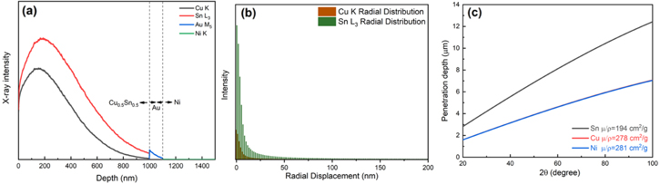
Figure 9. (a) MC simulation (Casino v2.48, 50,000 electrons, 20 keV) of the emission intensity of characteristic X-rays for Cu, Sn, Au, and Ni at different depths of the film; (b) radial distribution of the CuK and SnL3 characteristic X-ray intensity; (c) calculated X-ray penetration depth (>1% incident beam intensity) along the normal of the sample for the Bragg-Brentano  −
− diffraction geometry with incident X-ray energy (9 keV) slightly higher than Cu K
 based on mass attenuation coefficients from NIST tables.48
Download figure:
Standard image High-resolution imageThe XRD profiles of the Cu–Sn films are shown in Fig. 10 and Fig. A·3. The ε-Cu3Sn phase was not present in any of the samples. As discussed in above, because of their similarity in the crystal structure, the characteristic peaks of different Cu–Sn phases are difficult to distinguish (β, γ, δ), except for the phases with superlattice diffraction of the (3 1 1) plane for η'(Cu6Sn5) or (0 1 1) plane for η-Cu6Sn5 at 2θ ≈ 30°, the structures of which are shown in Fig. 11. Considering the possibility of preferred orientation formation for the intermetallic phases, and the large tolerance for their composition variance,49,50 the phase constitution analysis is not definitive. Considering the EDS analysis, the phase composition of each film has been proposed and summarized in Table IV. From the XRD results (Fig. A·3) the samples S4D-P and S4D-G, which are deposited below the reduction peak at −0.60 VAg/AgCl, limited β-Sn phase was observed, suggesting that the nucleation of β-Sn phase is inhibited by the competition for Sn by η' the and δ phases.51

Figure 10. XRD profiles of electrodeposited Cu–Sn alloys.
Download figure:
Standard image High-resolution image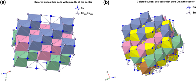
Figure 11. Crystal structures of (a) η (ICSD-52682) and (b) η' (ICSD-106530) phases. Note that the bcc-units with a Cu atom at the center are portraited as solid cubes. Different colors indicate different layers of bcc-001 planes, while additional bcc sites of the low temperature η' phase at each layer is colored specifically in yellow. The vacancies at the body centers break the original symmetry and give rise to bcc-001 diffraction51 Considering the large percentage volume difference of Cu and Sn, Ωsf = +83.4%,52 vacancies might be generated by the compressive stress on Cu and a large variation of the size of bcc units may occur due to ordering originated by dissolved Sn in the β matrix.
Download figure:
Standard image High-resolution imageTable IV. Elemental composition and phase composition of the deposits.
| Sample | Potential | Plan-view composition | Line-scan steady-state composition | Phases composition |
|---|---|---|---|---|
| S4A-P | −0.25 
|

|
— |

|
| S4A-G | ∼ −0.25 
|

|
— |

|
| S4B-P | −0.40 
|

|

|

|
| S4B-G | ∼ −0.40 
|

|

|

|
| S4C-P | −0.55 
|

|

|

|
| S4C-G | ∼ −0.55 
|

|

|

|
| S4D-P | −0.65 
|

|
— |

|
| S4D-G | ∼ −0.65 
|

|
— |

|
| S6C-P | −0.55 
|

|
— |

|
| S6C-G | ∼ −0.55 
|

|
— |

|
Analysis of the deposits listed in Table IV shows that the deposition condition (S4B-P and S4B-G), bath constitution (S6C-P and S4C-P), and applied potential (S4B-P, S4C-P) could drastically influence the phase constitution and composition of the film (as summarized in Fig. 12). All films are compositionally uniform under x20k plane-view observation except for deposition from bath S6, which shows a compositional variance as large as  (Fig. A·2).
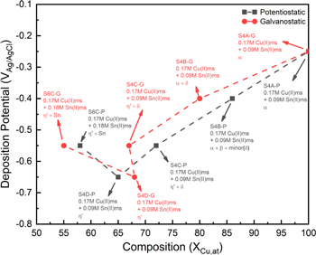
Figure 12. Composition-potential diagram for all the deposited Cu–Sn films.
Download figure:
Standard image High-resolution imageWhen comparing the XRD profile of sample S4B-G with the phase Cu41Sn11 (ICSD-439), several superlattice peaks at a low angle, especially (333) at 2θ = 26°, are absent or weak. As shown in Figs. 13a, 13b, the crystal structure of Cu41Sn11 is the 2 × 2 "bcc" stacking of 4 types of cantellated tetrahedrons. By setting the occupancy of all sites to the same type of atom in CrystalDiffract, and neglecting the atomic displacement, the simulated XRD pattern of fully disordered Cu41Sn11 is shown in Fig. 13c. It is noted that the fully disordered Cu41Sn11 structure does not show the strong superlattice peak of (333) compared with the original structure. To further determine if the superlattice peak (444) derives from the "bcc" stacking of Cu41Sn11, we use the atomic position of a single type of the cantellated tetrahedrons and increase the symmetry to I-43m based on the site symmetry of individual polyhedrons, the crystallography data of which are listed in Fig. 13b. It could also be seen that for simulated I-43m stacking, several superlattice peaks around 2θ = 29° are fainter, suggesting that these planar periodicities Cu41Sn11 are generated by the size difference between different polyhedron type.52

Figure 13. (a) the coordination structure of the cantellated tetrahedrons in δ phase (or cuboctahedron with only Td symmetry); (b) structure of individual cantellated tetrahedrons, with compositions of its four types in Cu41Sn11(ICSD-439) and the simulated fully disordered phase with higher (I-43m) symmetry; and (c) comparison of the XRD profiles between S4B-G, Cu41Sn11 (ICSD-439), simulated fully disordered ICSD-439 structure, and simulated fully disordered I-43m phase.
Download figure:
Standard image High-resolution imageFilm morphology
Figure 14 presents the morphology of Cu–Sn films. Deposit S4B-P consists of highly faceted and apparently large grains with a size about 200−300 nm. Considering the XRD data, these large grains should be β(bcc) phase. Faceting of bcc sub-μm particles (e.g. Nb53 and Fe54–56) exhibit the shape of rhombic dodecahedra,57,58 as exemplified by the β(bcc) phase in S4B-P (Figs. 14a, 14g): the orientation of these pyramids should be (011). A smaller fraction of (001) planes may indicate the slower relative growth rate of (011) planes compared with (001) planes for β(bcc) phase. Sample S4B-G in Figs. 14b, 14h, presents quite different features from the potentiostatic counterpart, both in terms of phase constitution and morphology, despite a very close composition. S4B-G mainly consists of large clusters of size about 500 nm, with each cluster consisting of grains about 10–20 nm. Very few reports discuss that electrodeposition mode (Potentiostatic or Galvanostatic) could influence the phase composition of the films.59–62 It is uncertain so far whether differences in the phase constitution are dominated by the nucleation behavior or by the elemental composition, due to the fluctuation of potential caused by the feedback loop necessary to control the Galvanostatic deposition mode.

Figure 14. SEM images (top: x5k, bottom: x40k) of (a), (g) S4B-P, (b), (h) S4B-G, (c), (i) S4C-P, (d), (j) S4C-G, (e), (k) S6C-P, and (f), (l) S6C-G.
Download figure:
Standard image High-resolution imageThe morphology of Cu–Sn alloys deposited at higher overpotential (S4C-P, Figs. 14c, 14i) or higher current (S4C-G, Figs. 14d, 14j) however behave similarly. Both sets show a rough surface consisting of abnormally large grains with size ∼ 1–2 μm on top of the film, and small grains with a diameter of less than 1 μm at the bottom. Each grain shows a cauliflower shape, probably originated by agglomeration and growth of individual nuclei at high overpotential.42,63–66 In contrast, potentiostatically deposited film S4C-P exhibit abnormally large grains at the top of the film compared with its counterpart S4C-G, implying some difference between Galvanostatic and Potentiostatic electrodeposition, despite both modes are designed to have the same steady-state deposition current.67
Deposits from bath # 6 show small differences between Potentiostatically (S6C-P, Figs. 14e, 14k) and Galvanostatically (S6C-P, Figs. 14f, 14l) deposited films at the same steady-state current as they exhibit similar morphology. Both samples contain ribbon-like grains and spherical grains, which are likely to be β-Sn68 and Cu-rich phases, respectively. However, the SEM-EDS data reveal that the correlation between these structures with the elemental distribution is not clear-cut, probably caused by the large sampling volume (depth ∼300 nm) of the EDS measurement with an acceleration voltage of 20 keV.
SEM cross-section observations
In order to determine the compositional distribution along with the thickness of the film, the sample was cut, ground and polished along its cross-section surface. The thickness of the deposit from bath # 4 is around 1–1.5 μm, while the thickness of deposits from bath # 6 is around 3 μm. SEM-EDS line-scans of the films were performed with an acceleration voltage of 20 kV, as shown in Fig. 15, with a sampling width as far as 50 nm (Fig. 16b). Using the signal from the Au layer as the reference, the Au peak in the line scan is broadened and slightly shifted, which is attributed to the spatial resolution of the e-beam interaction volume (Fig. A·2) and the drift of the sample. For samples S4C and S6C, the initial growth stage terminated within the first 0.5  and proved to be Cu-rich, suggesting a significant difference between the charge-transfer kinetics for Cu(II) vs Sn(II). The steady-state composition through the top 0.5
  m of the films is listed in Table IV, except for samples from S6C, due to its significant inhomogeneity. The samples S4C and S6C are rich in Cu compared with the steady-state compositions, probably caused by the SEM-EDS sampling of the initial Cu-rich stage (Fig. 16a). Considering this effect, a film composition close to Cu:Sn = 2:1 was achieved at the steady-state in samples S4C-P and S4C-G. For S4D samples, despite that the composition is close to 2:1, the films are rough even under visual inspection and thus was not considered to be good films.
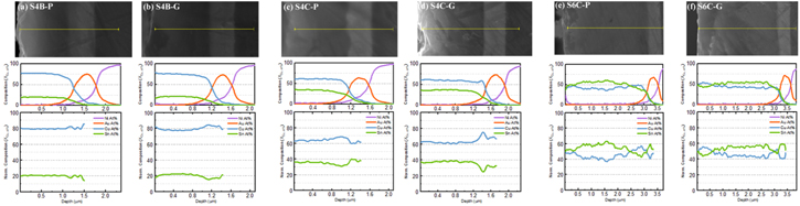
Figure 15. SEM-EDS line-scan of the cross-sections of the sample (a) S4B-P, (b) S4B-G, (c)S4C-P, (d) S4C-G, (e) S6C-P and (f) S6C-G. Raw data was smoothed using Fourier filter in OriginPro 2018 with a low-pass cutoff frequency corresponding to the wavelength ∼90 nm.67
Download figure:
Standard image High-resolution image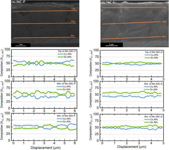
Figure 16. Inhomogeneity of samples (a) S6C-P and (b) S6C-G.
Download figure:
Standard image High-resolution imageHowever, when more Sn(II) was added to the bath, at the same deposition potential, significant compositional inhomogeneity could be observed in both plan-view SEM-EDS mapping (Fig. A·1) and line-scan perpendicular to (Figs. 15d, 15e) or along the films (Fig. 16) for the S6C-P and S6C-G samples. Along the film, large variations of the composition could be observed, with the scale from 200–700 nm at the top of the film, to 1.5 μm at the bottom of the film with small fluctuations around 200 nm. The average composition is about 50%Cu, at at the top of both films, with a composition fluctuation of about 10%–20%. An initial Cu-rich region could be observed for both samples at the bottom of the films.
Discussion
As seen in Fig. 15, due to the high Cu deposition overpotential and transient Cu concentration at the surface, a Cu-rich layer initially grows quickly, until reaching a film thickness of around 0.5 um under the deposition conditions of samples S4C and S6C. This compositional gradient is generated by the depletion of the surface metal ions, after which a steady-state would be reached, resulting in a relatively steady film composition along the film. The initial layer thickness is unavoidable when conventional electrodeposition is used; however, this could be minimized by using a low concentration bath or using for instance pulse electrodeposition.
Sn deposition starts to occur at −0.40 VAg/AgCl based on the CV scans. In presence of Cu ions, however, ∼ 20% of Sn in the samples S4B grow via underpotential condition due to the enthalpic contribution of the Cu–Sn intermetallic phases compared with  and
and  reference phases. From CALPHAD data in Fig. 15b, formation of metastable disordered bcc or bcc-derived phases instead of hcp-derived phase
  phase could be possibly caused by the favored energetics or nucleation kinetics of precursor disordered bcc phase vs disordered fcc or hcp phases.
At high overpotential, the film composition is close to the metal ion ratio in solution; this suggests that during 4 min of deposition from the bath-4 the system is able to reach the limiting current deposition composition, with a mass-transfer coefficient ratio close to 1.
A large composition fluctuation is observed in the S6C depositions, supporting the XRD results that these films consists of two-phase mixture of Sn-rich and Cu-rich phases; this is reasonable, considering the high Sn content in the deposition bath and the large Sn overpotential, enabling Sn to nucleate, grow independently, and competing with the Cu-rich phases η' or η.
Conclusions
In conclusion, we have demonstrated that it is possible to produce a cyanide-free electrodeposition bath for white bronze alloys, based on alternative organic additives and an eco-friendly electrolyte.
We have found that nitrilotriacetic acid, a commonly water-insoluble component, is solubilized in presence of Hydroquinone, and we did find that - despite the low value of the solution pH, the complexing agents are able to bond metal ions showing a suppressing behavior for copper. In addition, two stable deposition solutions were identified with Cu:Sn molar ratio in solution respectively of 1:1 and 1:2.
Utilizing the solution with a Cu:Sn molar ratio of 1:1 and a deposition potential of −0.55 V, EDS and XRD data confirmed the formation of a η' single-phase bronze with a Cu:Sn composition ≈ 2:1. Moreover, the SEM cross-section analyses showed a relatively uniform composition of this film. The elemental composition and the crystal structure of the films with deposition condition of S4B make this electrodeposition approach a promising candidate for the synthesis of kesterite compounds.
Acknowledgments
LF thanks the CRIST (Laboratory of Structural Crystallography), University of Florence, for the additional XRD measurements needed to refine the characterization work.
YKS thanks Adam Thompson in Prof. James Burns' group at DMSE, University of Virginia for the discussion about SEM-EDS cross-section spatial resolution, and Richard White at DMSE, University of Virginia for the simple-but-elegant cross-section epoxy clamps.
Appendix
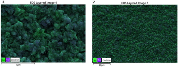
Figure A·1. Segregation of Sn and Cu in sample (a) S6C-P and (b) S6C-G by SEM-EDS mapping.
Download figure:
Standard image High-resolution image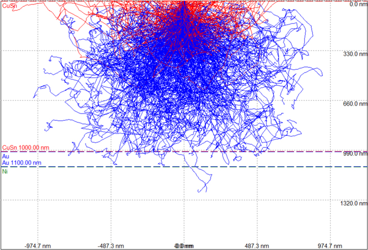
Figure A·2. Interaction volume of 20 keV e-beam with Cu0.5Sn0.5, with red trace indicates backscattered electrons and blue traces for secondary electrons. Droplet shape of the affected area could be observed, which lowers the spatial resolution and serves as major reason for peak broadening of Au layer in cross-section samples (Fig. 15).
Download figure:
Standard image High-resolution image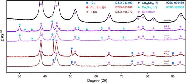
Figure A·3. XRD profile for the films S4A-P, S4A-G, S4D-P, and S4D-G, XRD data of the substrate was collected using a Bruker (Billerica, MA) New D8 Da Vinci Diffractometer with Cu Kα radiation, Ni filter, fast multichannel energy-discriminator detector, flat holder and Bragg-Brentano configuration (CRIST, University of Florence).
Download figure:
Standard image High-resolution image