
Abstract
The addition of zinc oxide (ZnO) nanoparticles into electroluminescent poly(vinylcarbazole) (PVK) polymer layers results in increased current densities, brightness, and luminance efficiencies in polymer light emitting devices. For low turn-on voltages, an increase in current density and good stability are achieved. At 9 V, we achieved a brightness of  with a luminance efficiency of 0.35 cd/A for PVK–ZnO nanocomposite devices. Electroluminescence (EL) spectra reveal that the EL yield of PVK–ZnO nanoparticle devices increased greatly as compared with pure PVK devices. The current–voltage characteristics indicate that the addition of ZnO nanoparticles can facilitate better electrical injection and charge transport.
Export citation and abstract BibTeX RIS
The development of organic devices has been driven by a growing demand for low cost and flexible electronic devices and information displays. Polymer light emitting diodes (PLEDs) using solution processes can be promising candidates for large-area, fast-response, and flexible displays. Major technological issues related to commercial applications are quantum efficiency, device stability, and ease of fabrication. However, the potential use of electroluminescent devices is ultimately limited by their low quantum efficiency as well as their poor stability. Despite these critical drawbacks, the polymer light emitting devices still receive considerable attention due to several merits: ease of fabrication with low cost, low operating voltage, flexibility, etc. Therefore, many researchers have focused on solving the problem of low efficiency and poor stability. One of the major reasons for the low quantum efficiency of single layer PLEDs is that electron injection is more difficult than hole injection in most polymer light emitting devices due to the high energy barrier for electron injection and low electron mobility in most conjugated polymers. Therefore, one of the most important challenges in the field of PLEDs is to balance the charge carrier injection that is essential for high efficiency. Charge carrier mobility plays an important role in determining the device electroluminance performance, which is closely related to the balance of holes and electrons for injection and transport.1–6 To enhance luminance efficiency, optimum charge carrier mobility is required. One way to overcome the electron injection and transport limitations is to combine polymers with inorganic semiconductor particles that have low energy barrier for electron injection and high electron mobility. Polymer–nanoparticle composites have emerged as a class of materials for optoelectronic devices such as luminescent devices,7–9 thin film transistors,10 photovoltaic devices,11 and optical waveguides.12 Nanocomposites of conjugated polymers with inorganic oxides provide the possibility of tuning the morphology and optoelectronic properties. In addition, they could be used to improve the poor thermal and mechanical stability of conjugated polymers for device applications.
Efficient charge injection and transport are important aspects in composite nanoparticle-based polymer electroluminescent devices. The electrons and holes injected from respective electrodes combine inside nanoparticle and/or polymer layers, with a characteristic light being emitted as a result of the recombination of these carriers. The electron and hole currents flowing across the electroluminescence (EL) devices are mainly determined by the energy levels of the individual components of the EL device. The location of recombination and device efficiency are controlled by the mismatch of these energy levels. In general, improved device efficiency can be accomplished by adding electron transport layers and/or hole transport layers.13 Colvin et al.8 demonstrated that a double layer structure having separate poly( -phenylene vinylene) (PPV) and CdSe nanocrystal layers did not exhibit detectable EL emission. Yang et al.9 reported that a poly(3,4-ethylenedioxythiophene) (PEDOT):poly(styrene sulfonate) (PSS) layer containing nanocrystalline ZnS:Mn led to enhanced current flow through the device because of a lower energy barrier for hole injection from the indium tin oxide (ITO) anode as well as enhanced hole mobility in PEDOT:PSS. Bozano et al.14 investigated that charged nanoparticles assembled at a semiconducting polymer poly[2-methoxy-5-(2-ethyl-hexyloxy)-para-phenylene vinylene] (MEH-PPV)–electrode (Ca) interface could dramatically improve the electroluminescent properties because they effectively increased the local electric field and promoted carrier injection. Lee et al.15 reported polymer (MEH-PPV)–clay nanocomposite materials for luminescent devices. The luminescence efficiency and environmental stability were significantly improved as the two-dimensional layered silicate could prevent exciton formation by intercalation and decrease the penetration of oxygen and moisture into the emissive layer.
In this work, composite materials consisting of conjugated polymers and metal oxide nanoparticles are the focus of interest due to their physical, electronic, and optical properties. An n-type semiconductor material ZnO, possessing a direct wide bandgap (3.2 eV) and large exciton binding energy (60 meV) with strong piezoelectric and pyroelectric properties, was used to make the composite with a conjugated polymer poly(vinylcarbazole) (PVK). ZnO is one of the most promising candidates for the fabrication of short-wavelength optoelectronic devices.16–18 Here we report a ZnO nanoparticle and polymer nanocomposite for light emitting devices to improve electroluminescent characteristics.
Experimental
PVK was purchased from Sigma-Aldrich Chemical and used without further purification. Patterned ITO-coated glass substrates were cleaned with detergent, distilled water, acetone, and 2-propanol and subsequently in ultrasonic bath. The substrates were dried in an oven at  before treatment with UV ozone. After treatment with UV ozone for 25 min, a 40 nm layer of PEDOT:PSS was spin-coated onto the substrates, followed by drying on a hot plate at
  for 30 min. The commercially available ZnO nanorods with 30–50 nm diameter and
  length were purchased from Sigma-Aldrich Corporation. The weight ratios of PVK vs ZnO were changed from 10:1 to 1:1 for PVK–ZnO (10:1 by wt %), PVK–ZnO (5:1 by wt %), and PVK–ZnO (1:1 by wt %). The polymer light emitting devices of the PVK–ZnO composite single layer were fabricated as follows: PVK and ZnO were predissolved in toluene and mixed well to give different volume ratios. Composite single layers of PVK–ZnO were spin-coated from toluene solutions with a speed of 2000 rpm for 1 min on top of the PEDOT:PSS, followed by baking on a hot plate at
  for 30 min inside a glove box. Then, the poly(ethylene oxide) (PEO) (5 nm), Ca (60 nm), and Al (120 nm) electrodes were thermally evaporated in a vacuum of
  . For the measurement of device characteristics, current density–voltage–luminance
  changes were measured using a power supply (Keithley 2400) and a fluorescence spectrophotometer (Ocean Optics USB 2000). The luminance was further corrected by a Spectra-Scan PR650 spectrophotometer. An atomic force microscope (AFM, DI dimension 3100) was used to monitor the surface morphology of the films. The active area of the EL devices that overlapped between ITO and the cathode electrodes was
  . The device structure is shown in Fig. 1.

Figure 1. Device configuration of the nanocomposite device ITO/PEDOT:PSS/PVK:ZnO/PEO/Ca/Al.
Results and Discussion
Figure 2a and 2b shows the  and
and  characteristics of the devices. The turn-on voltage, defined as the bias voltage applied to a device producing a brightness of
  , for the PVK device is 6.5 V, whereas that for the PVK–ZnO (1:1), PVK–ZnO (5:1), and PVK–ZnO (10:1) devices are 5, 5.8, and 6.3 V, respectively. The maximal luminance is best achieved in the weight ratio of 10:1 of PVK:ZnO. It is
  (at 9 V). However, the maximal luminance for the weight ratio of 1:1 and 5:1 is
  (10 V) and
  (8.5 V), respectively.

Figure 2. (a)  and (b)
  characteristics of PVK, PVK–ZnO(1:1), PVK–ZnO (5:1), and PVK–ZnO (10:1) devices. The inset shows a detailed view of (b).
The maximum brightness of the PVK device has been observed with current 37.19 mA (8.9 V), whereas same brightness is achieved at currents 10.2 mA (8.5 V), 8.73 mA (6.9 V), and 7.55 mA(7.5 V) for the PVK–ZnO (1:1), PVK–ZnO (5:1), and PVK–ZnO (10:1) devices, respectively, corresponding to 3.65-, 4.3-, and 4.9-fold improvement of current efficiency. These results indicate that the large increase in current efficiency going from pristine PVK to PVK–ZnO as the active layer was achieved by improving the carrier injection and charge carrier balance in the devices.
Figure 3a shows the luminance efficiency of PVK and PVK–ZnO nanoparticle composite devices. The best performance with a maximum luminance efficiency of 0.35 cd/A at 9 V was found in the PVK–ZnO (10:1) composite, which is greater as compared to that reported in PVK–CdSe polymer–nanocrystal hybrid light emitting diode (LED) (0.078 cd/A),19 white emission polymer–nanocrystal composite 2-(4-biphenyl)-5-(4-tert-butylphenyl)-1, 3,4-oxdiazole–CdTe LED (0.068 cd/A),20 and PVK–near-IR dye–CdSe/CdS based quantum dot PLED (0.002 cd/A).21 Figure 3b shows the electroluminescent spectra of devices with different wt % of ZnO to PVK. As a reference, the PVK-only device is also shown in Fig. 3b. As compared to the PVK-only device, the bandwidth of the EL emission from the device, PVK–ZnO (10:1), is obviously broadened. In addition, there is no trend in the EL emission peaks toward longer wavelengths with increasing ZnO wt %. For example, the PVK-only film has a peak at 440.1 nm, the (10:1) blend film has a peak at 446.0 nm, and then again it shifts back to 440.7 nm as the ZnO wt % increases (5:1), which is exactly the same peak of a PVK film. These results demonstrate that the emission of device PVK–ZnO (10:1) is from both ZnO particles and PVK due to electron–hole recombination in both components. This is the case for most nanoparticle/polymer hybrid devices.22, 23

Figure 3. (a) The luminescence efficiency vs voltage curves. (b) Normalized EL spectrum of characteristics of PVK, PVK–ZnO (1:1), PVK–ZnO (5:1), and PVK–ZnO (10:1) devices.
To examine the effect of nanoparticles on PLED lifetime, the decay of the EL intensity as a function of time was measured with a current of 10 mA. As shown in Fig. 4, the EL peak intensity for the nanoparticle-containing device drastically reduced. It is similar to the degradation phenomenon occurring in PLEDs.24

Figure 4. EL intensity decay profiles of the PVK–ZnO nanoparticle composite devices with different weight ratios. The inset shows an energy-level diagram of the nanocomposite device ITO/PEDOT:PSS/PVK:ZnO/PEO/Ca/Al.
The increased current by the addition of ZnO nanoparticles may be attributed partly to the ease of charge transport. The ZnO nanoparticles dispersed in the polymer may reduce the barrier for hopping, which may cause an increase in carrier density. The enhancement of charge injection and transport may play their roles together for the enhancement of EL property by the addition of ZnO nanoparticles. To understand the role of ZnO nanoparticles in devices, the energy-level diagram of the device is shown in the inset of Fig. 4. The highest occupied molecular orbital (HOMO) and lowest unoccupied molecular orbital levels of PVK were 5.8 and 2.3 eV, respectively.25 The valence (7.6 eV) and conduction (4.4 eV) 26 bands of ZnO show a clear indication that an energy barrier exists for a few holes to be transferred from PVK to ZnO. PVK molecular chain was made more unwindable due to the dispersing ZnO nanoparticle, which induced efficient charge transport along the chain. The connection between aligned molecular chains of PVK on ZnO nanoparticle can also increase carrier transport in nanocomposites. Thus, the current would not be limited by hopping of carriers between chains. Additionally, ZnO can also improve the hole transporting ability of the PVK layer because of the higher mobility of ZnO nanoparticles.
Figure 5 shows the surface topography images of the four films coated on the same substrate ITO/PEDOT: (a) PVK layer, (b) PVK–ZnO (1:1), (c) PVK–ZnO (5:1), and (d) PVK–ZnO (10:1). The roughness of the surface of the spin-coated sample film changed significantly. The increased roughness caused by the capillary attraction between the polymer and the ZnO nanoparticles increased the interfacial area between the sample film and the PEO/Ca/Al cathode and thus facilitated electron injection. The root-mean-square roughness values of the films are PVK (0.862 nm), PVK–ZnO (1:1) (3.505 nm), PVK–ZnO (5:1) (2.291 nm), and PVK–ZnO (10:1) (1.9 nm). A similar effect on surface roughness has been observed by other researchers in  and poly(9,9-dioctylfluorene-alt-thiophene copolymer/Au nanocomposite films, and the performance of their device was improved by the addition of
  and/or Au nanoparticles.27, 28

Figure 5. AFM three-dimensional images of (a) PVK, (b) PVK–ZnO (1:1), (c) PVK–ZnO (5:1), and (d) PVK–ZnO (10:1) devices.
The mechanism for the current density and luminance enhancement in a polymer–nanoparticle-based LED is not yet fully understood. Carter and Blom et al.28, 29 suggested that the change in morphology leads to both enhanced current density and radiance in polymer–nanoparticle LEDs. When nanoparticles are spun and mixed into a solution with the active polymer layer, strong electrostatic forces attract the nanoparticles to the anode and to the polymer in which it is mixed. The polymer solution is then drawn around the nanoparticles into cavities, which result in rough surfaces, onto which the cathode is evaporated. Thus, producing a rough interface between the cathode and the composite film leads to a significant increase in surface area as well as electron injection. Additionally, higher current densities and device radiances can result from effective thin spots, which are formed from the capillary forces in the nanoparticle incorporation process. Furthermore, the existence of thin spots created throughout the film by capillary forces would give rise to an increase in the electric field, enhancing the charge injection and/or charge transport.
To study the charge injection mechanism under direct current bias, we considered Richardson–Schottky thermionic emission and Fowler–Nordheim (FN) tunneling models. The  characteristics are determined by the FN tunneling equation of both electrons and holes through contact barriers arising from the band offset between the polymer and the electrodes. Furthermore, at low fields the tunneling model was found not applicable to the experimental
  characteristics, which has been attributed to the contribution of thermionic emission to the current and to band-bending effects at the interface. The tunneling current by the FN model is expressed as30

where  is the applied electric field
  in which
  is the active layer thickness,
  is the effective charge carrier mass,
  is the electronic charge, θ is the barrier height, and
  is Planck's constant.
  is the rate coefficient of tunneling containing prefactors and the rate of current backflow. Equation 1 can be written in the form
and  is a parameter that is related to the shape of the injection barrier height, where

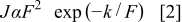
Figure 6 shows a plot of  vs
vs  for our devices at different wt % of ZnO doped in PVK. A straight line is clearly observed, indicating that the injection is indeed tunneling. As the weight percentage of ZnO is increased, the θ values [0.71, 0.67, 0.65, and 0.30 eV for PVK, PVK–ZnO (10:1), PVK–ZnO (5:1), and PVK–ZnO (1:1), respectively] tend to decrease. From the slope of the straight line, corresponding to the region in the
  characteristics of Fig. 2a, we can determine the barrier height to hole injection. For all devices, barrier height is estimated to be
  to 0.71 eV. The estimated barrier height is higher than the actual value of 0.6 eV between the HOMOs of PEDOT and PVK. This indicates that the current is not a simple hole injection.31
Figure 6. FN plot of (a) PVK, (b) PVK–ZnO (1:1), (c) PVK–ZnO (5:1), and (d) PVK–ZnO (10:1) devices.
As the electric field is increased to a higher biased voltage, the FN curve deviated from the predicted line, suggesting the accumulation of space charge at the polymer/cathode interface. Although the electric field is increased to a higher biased voltage, electrons start to be injected into the PVK layer and the recombination of opposite charge carriers occurs. This part of the bias regime is no longer valid for FN tunneling prediction for the single carrier.
Conclusion
In summary, polymer light emitting devices based on ZnO-nanoparticle-doped PVK polymer materials have been technically prepared by the solution-based spin-coating technique.  and brightness–voltage characteristics demonstrated that the ZnO nanoparticles have the ability to improve current density and brightness, which may be caused by the enhancement of charge injection and charge transport. In addition, the ZnO nanoparticles appear to modify the device interfacial morphology, which facilitates electron injection, improving both the EL lifetime and the luminance efficiency of a PLED simultaneously. The PVK–ZnO nanoparticle composite devices have current efficiencies higher than that of the pristine PVK devices. Because of the simple device structure and easy control of fabrication conditions, this method has a high potential for the practical application of flat panel displays.
Acknowledgment
The authors thank the Office of Research and Development, National Cheng Kung University.
National Cheng Kung University assisted in meeting the publication costs of this article.