
Abstract
Low temperature (ranging from  ) metal induced lateral crystallization of Ge using germanide forming metals Ni, Co, and Pd is performed. The lateral growth lengths and crystallized Ge films' quality are optimized when annealed at
  , above which self-nucleation in Ge hinders the metal induced crystallization process. At
  , the sample with Pd as the seed metal has the largest lateral growth length, while the sample using Co as the seed layer exhibits the largest crystal grain size. The experiments suggest that the lateral growth length is associated with the diffusivity of the metal and germanide in Ge, while the crystal quality is related to the lattice mismatch between germanide and Ge.
Export citation and abstract BibTeX RIS
Polycrystalline germanium (poly-Ge) on insulator and low cost substrates has many potential applications in solar cell, optoelectronics, and three-dimensional integrated circuit (3D-IC). With a small bandgap of  at room temperature, poly-Ge can be employed in a thin-film tandem solar cell to enhance the absorption of the IR spectrum. It can also be used in optical detectors of 1.3 and
  wavelength. Vertical transistors stacking in a 3D-IC structure is expected to lessen performance degradation due to interconnects delay and power dissipation. Poly-Ge is a promising material for active layers in this 3D-IC architecture because of their high mobilities1 and lower crystallization temperatures as compared to Si.2 For poly-Ge to be integrated on top of existing devices or low cost substrates in optoelectronic and integrated circuit applications, it should be crystallized at low temperature, preferably below
  .
.
Crystallization of deposited amorphous Ge (a-Ge) can be performed by various techniques, three of which are often discussed: laser anneal, solid-phase crystallization, and metal induced (lateral) crystallization (MIC/MILC). While laser anneal gives a high quality Ge due to local heating without damaging the underlying layers, this technique is complex and expensive. Conversely, conventional solid-phase crystallization of Ge requires a relatively long anneal time and a high temperature of around  .3, 4 A longer incubation time is needed for a lower anneal temperature.5 MIC/MILC is similar to solid-phase crystallization, but in this method, metals are deposited on top of or inside Ge to enhance the crystallization of Ge, with a possible reduction of the crystallization temperature to as low as
  .6 MIC and MILC are the crystallization of regions inside and outside the metal coverage, respectively. Due to the lesser metal contaminant and larger grain size in the MILC region, it is preferable over MIC.
The MILC of Si has been extensively studied, and the preferred metal is Ni due to the small lattice mismatch between  and Si. However, fewer works were done on Ge, in which the choice of seed metal is still not obvious. Metals used in the MILC process can be categorized into two groups: the first (Co, Ni, Pd, etc.) forms a germanide and the second (Au, Ag, Al, etc.) creates a eutectic with Ge. Focusing on the first metal group, we carried out low temperature (from
  ) MILC of Ge using Co, Ni, and Pd as seed metals. The MILC of Ge with varied temperatures using Ni, Co, and Pd were separately reported by Kanno et al. ,2 Park et al. ,7, 8 and Xie et al.9 In Ref. 2, which investigated the MILC of Ge using Ni, the lateral growth rates at different temperatures were reported, but the quality of the film was not mentioned. In the studies on the MILC of Ge using Ni 7 and Co,8 the growth rates at different temperatures were not described. Moreover, it is difficult to compare the poly-Ge properties of these works because the deposition and annealing processes were different. Thus, in this work, the MILC of Ge using Co, Ni, and Pd is carried out at varied temperatures from
  , after which the crystallization rates and the quality of the crystallized Ge films are analyzed and compared. To our knowledge, such a direct comparison on the crystallization rate and poly-Ge's quality for the three metals has not been reported. In addition, it is found that the quality of the crystallized film and the growth rate is not related, and hence the choice of metal to be used in the MILC process depends on the application of the crystallized film.
Experimental
After 
 was deposited on clean Si substrates using plasma-enhanced chemical vapor deposition, a thin layer of roughly
  Ge was sputtered from 99.999% Ge target at room temperature using radio-frequency sputtering with
  as plasma gas. A
  thick
thick  layer was then deposited to protect the Ge film from excessive oxidation and contaminant. The cross section of the structure at this stage is shown in Fig. 1a. Lithography and dry etching were used to define Ge patterns (Fig. 1b). Photoresist (PR) was then spin-coated and developed to open up windows for seed metals. The exposed underlying oxide was etched away using 1% diluted HF (Fig. 1c), immediately followed by the deposition of about
  Ni, Pd, or Co by an E-beam evaporator (Fig. 1d). For the control samples, no metal was evaporated. Lift-off was carried out in acetone solution which was subjected to ultrasonic treatment, where the PR and the metals on top of the PR were removed (Fig. 1e). The samples were then annealed at 350, 375, 400, or
  in
in  ambient for
  , after which they were coated with a thin layer of oxide to reduce any possible reaction with the atmosphere. Finally, the samples were characterized using optical microscopy, Raman spectroscopy, and atomic force microscopy (AFM). Figure 1f shows the top view of the structure studied in this work. The MIC region where the seed metal was deposited is located at the center. The line structures with different widths on the left are used to study the effect of the structure's width on the lateral growth rate, and the plane structure on the right is used to determine the MILC rate in an unconfined area.
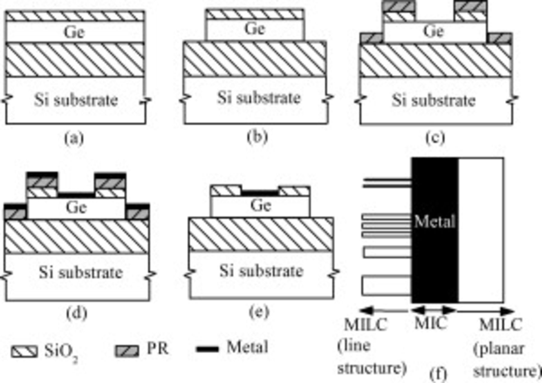
Figure 1. Structure fabrication flow: (a) Ge and  deposition, (b) patterning of Ge, (c) PR spin-coating and developing, (d) metal deposition, and (e) lift-off process. (f) Top view of the final structure.
Results and Discussion
An optical microscope was used to observe and capture the images of the MIC and MILC regions on Ge samples after the anneal, for example, the images of Ge (Pd) and Ge (Ni) samples shown in Fig. 2. In this paper we denote Ge samples using seed metal M as Ge (M), where M is Ni, Pd, or Co. From the images, the different MIC, MILC, and amorphous regions can be clearly seen by comparing their contrasts and colors. For each seed metal and different temperature, the average MILC lengths, defined as the perpendicular distance from the MIC region to the MILC amorphous interface, were calculated from 50 measurements. The results are compiled in Fig. 3. It is observed that the MILC lengths reach maxima when Ge samples were annealed at  . At the optimal anneal temperature of
  , the MILC rates of Ge (Ni) and Ge (Pd) are similar (about
  ), which are more than two times faster than Ge (Co)'s MILC rate. At 400 and
  , no lateral growth is observed in Ge (Co). The MILC growth rate of Ge (Ni) at
  is considerably slower than the
  reported by Kanno et al.2 This is because in Ref. 2, the self-nucleation in Ge only started after incubating at
  for almost a thousand minutes. However, in this study, self-nucleation already occurred when the Ge films were annealed at
  for only
  (see the Raman spectra in Fig. 5a). When the annealing temperature is above
  , self-nucleation slows down the MILC process, which is consistent with reports by Ref. 2.

Figure 2. Optical microscope image of (a) Ge (Pd) and (b) Ge (Ni) samples.
Figure 3. MILC lengths after  anneal at different temperatures for Co, Pd, and Ni.
The MILC lengths in the line structures are found to be dependent on their widths. In Ge (Pd) and Ge (Ni) samples annealed at  , 10 MILC lengths were measured and averaged for each width (see Fig. 2), ranging from
  . A scanning electron microscope image of a
  wide Ge (Pd) line structure shows an MILC length of about
  . The compiled data are presented in Fig. 4. It is seen from Fig. 4 that as the width decreases, the MILC lengths increase to maxima before they drop. Park et al. also reported that for the MILC of Ge using Ni, lateral growth rate reduced from
  in a plane structure to
  in a
in a  wide line structure,7 but the investigation on how the MILC rates varied with the linewidths was not carried out. As the line becomes narrower, the diffusion paths of the metal alloy are more aligned, resulting in a longer diffusion length. However, further reduction of the linewidth limits MILC growth because it lessens the amount of metal diffusing through the structure.
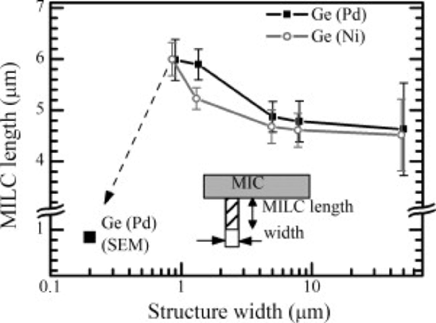
Figure 4. MILC lengths in Ge (Pd) and Ge (Ni) sample line structures with different linewidths. The samples were annealed at  .
.
Micro-Raman spectroscopy was used to characterize the quality of crystallized MIC and MILC Ge films. The Raman spectra of control Ge samples with no seed metal are shown in Fig. 5a. The line shapes of as-deposited Ge and control Ge samples annealed at 350 and  have peaks at around
  , indicating that the films are amorphous. However, the control samples annealed at 400 and
  have asymmetric peaks at around
  , indicating that self-nucleation in Ge has occurred. The line shapes of 400 and
  control samples both show two peaks when fitted with Lorentzian curves using a nonlinear regression method, one at around
  corresponding to an a-Ge phase and the other one at around
  , which is attributed to a nanocrystal with a grain size of less than
  . Using Eq. 1 10, 11 and integrated intensities under the fitted curves, the crystalline fractions of the control samples annealed at 400 and
  are estimated to be 72 and 80%, respectively
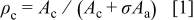
where  is the crystalline fraction,
  and
and  are the integrated intensities of the crystalline peak and the amorphous peak, respectively, and σ is the correction factor, estimated to be 0.8.10, 11
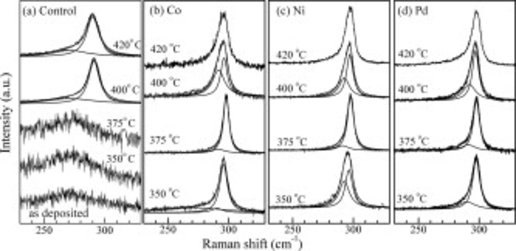
Figure 5. Raman scattering spectra measured on MIC regions of Ge samples annealed at various temperatures: (a) Control Ge samples without metal, (b) Ge (Co) samples, (c) Ge (Ni) samples, and (d) Ge (Pd) samples.
The Raman spectra measured on the MIC Ge regions are shown in Fig. 5b (Co samples), Fig. 5c (Ni samples), and Fig. 5d (Pd samples). The line shapes were also fitted into two or three Lorentzian curves using a nonlinear regression method depending on the goodness of the fit. The fitted curves peak at around 270, 297, and  corresponding to the a-Ge phase, large crystallite Ge phase with grain size larger than
  , and small crystallite existing at grain boundaries with grain size of less than
  , respectively. At
  , it can be seen from peak fitting that the Ge (Co) sample still contains an amorphous phase. Even though the Ge (Ni) is fully crystallized, its small crystallite's density is relatively higher than that of the Ge (Pd) sample, as shown by the stronger peak at
  . This trend is expected because compared to Ni and Co, Pd induces Ge crystallization at lower temperature.4 At
  , nonlinear Lorentzian fitting of MIC Ge spectra shows no amorphous peak, indicating that the MIC Ge films are fully crystallized. The Raman peak of MIC Ge induced by Co is significantly sharper than that by Pd and Ni, implying a larger grain formation in the MIC region of Ge (Co). Moreover, using the integrated intensity under the fitted curves, the approximated density of the large Ge crystallite (with peak at
  ) is 87% for Ge (Co), 84% for Ge (Ni), and 78% for Ge (Pd). Compared to Ge samples annealed at
  ,
,  shows stronger peaks at
  as well as broader Ge–Ge peaks at
  . As the temperature increases from
  , the approximated densities of small crystallites change from 13 to 55% for Co, from 16 to 39% for Ni, and from 22 to 40% for Pd. These changes are attributed to the self-nucleation effect in Ge at
  , which hinders the MIC/MILC process. Peak broadening is also observed in Ge samples annealed at
  . It can be seen that self-nucleation in Ge has the strongest effect on Co MIC and MILC, evidenced by the small density of large Ge crystallite (with grain size larger than
  ) and no observed lateral growth. Figure 6 shows the full width at half-maximum (fwhm) of the above fitted Lorentzian curves with peaks at around
  due to Ge–Ge optical phonon. For the three metals, the fwhm is smallest when annealed at
  . The Co samples' fwhm decreases significantly as the anneal temperature increases from
  .
.
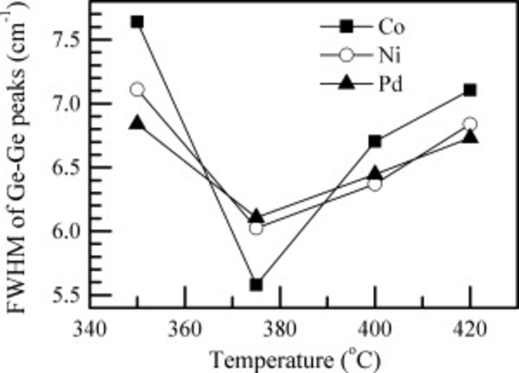
Figure 6. FWHM of Ge–Ge optical phonon peaks derived from nonlinear fitting the Raman spectra of MIC regions with Lorentzian curves.
The MILC of Ge using germanide forming metals (Ni, Co, and Pd) involves three processes: (1) Ge metal alloy formation, (2) diffusion of metal alloy, and (3) reaction of metal alloy with a-Ge resulting in crystallized Ge. For the germanide forming metal, the MIC process only starts after the germanide phase desirable for crystallization process is formed.12 Among the three metals studied, Pd and Ni diffuse faster and form an alloy at a lower temperature than Co.4, 13 Thus, the rates of processes 1 and 2 are expected to be higher in Pd and Ni samples than that in the Co sample. This explains the faster lateral growth shown in Pd samples. For process 3, the facets of crystalline germanide act as epitaxial planes for the crystallization of Ge. A smaller lattice mismatch between crystalline alloy facets and Ge planes is expected to speed up process 3, which not only enhances the crystallization rate, but also forms a larger grain size. With Co, Ni, and Pd, the germanide phases existing at  can be CoGe,
  ,
,  , NiGe,
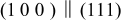
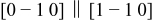
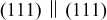
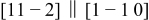
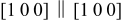
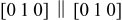
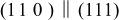
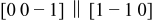
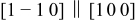
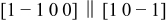
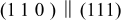
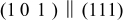
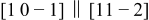
  , and PdGe. Their crystal structures and lattice constants are listed in Table I. Using these values, the possible epitaxial relations between germanide and Ge planes are calculated, and those relations with a small lattice mismatch are tabulated in Table II and illustrated in Fig. 7. In the Ni induced lateral crystallization of Ge, it was reported that ⟨111⟩ was one of the dominant growth directions.7 Our calculation suggests that Ge(111) is likely to be epitaxial to NiGe(110) with a lattice mismatch of only
  .
.
Table I. Crystal structures and lattice constants of Ge and germanide responsible for the MIC/MILC process.
| Pearson symbol | Type | Lattice constants (Å) | Reference | |||
|---|---|---|---|---|---|---|

|

|

| ||||
| Ge | cF8 | C(diamond) | 5.6575 | — | — | 18 |
| NiGe | oP8 | MnP | 5.81 | 5.38 | 3.43 | 19 |
| CoGe | cP8 | FeSi | 4.637 | — | — | 20 |

| oC24 | — | 5.670 | 5.670 | 1.0796 | 20 |

| tI24 | — | 7.64 | — | 5.81 | 20 |

| hP9 |

| 6.712 | — | 3.408 | 21 |
| PdGe | oP8 | MnP | 6.259 | 5.782 | 3.481 | 22 |
Table II. Possible epitaxial relations between germanide and Ge planes. The list is not exhaustive. Only matching planes with low lattice mismatch are presented.
| Epitaxial |

|

|
 (%) (%) |
 (%) (%) | ||||
|---|---|---|---|---|---|---|---|---|

| Ge |

| Ge |

| Ge | |||
| NiGe |

|
|
|

|

| |||
| NiGe |
|
|

|

|

| |||
| CoGe |
|

|
|

|

| |||

|

|
|
| 0.2 | 0.2 | |||

|

|

|

| 0.2 | 3.8 | |||

|
|
|
|

| 3.9 | |||

|
|
|
| 2.7 |

| |||

|

|
|
|

|

| |||

|
|
|
|

|

| |||
| PdGe |
|

|

| 6.5 | 0.5 | |||
| PdGe |
|

|
|

| 3.4 | |||
| PdGe |
|
|
| 4.3 |

| |||

Figure 7. Illustration of epitaxial relations between germanides and Ge. Empty circles (○) and black dots (●) represent germanide and Ge lattice points, respectively.
Considering Co samples annealed at 350 and  , while the MILC lengths increase slightly, their Raman spectra fwhm decrease significantly, suggesting that the rate of processes 1 and 2 in both samples are similar, but that of process 3 is drastically different. It could possibly be due to a change in the Co germanide phase responsible for the crystallization process. For a thin Co layer on a-Ge, Ashburn et al. reported that
  was formed at
  , after which it transformed into
  at
at  ,14 while Opsomer et al. showed that CoGe was formed at
  , after which it completely transformed into
  at
at  once Co was fully consumed.15 In both papers, the thickness of Co used was
  . However, in our case, because only a
  thick Co layer was deposited,
  is expected to be formed at a much lower temperature. Moreover, the lattice mismatches between CoGe,
  , and Ge are relatively large (about
  ), while the mismatch between
  and Ge is only 0.2% (refer to Table II). Together with the fact that the Raman spectrum of the Co sample annealed at
  is much sharper than those of the Ni and Pd counterparts, we deduce that
  is the phase responsible for the Ge crystallization process at
  , while the Co germanide phase at
  could be CoGe or
  .
.
In the Pd induced crystallization of Ge, it is believed that  is the germanide phase responsible for the crystallization process, in which the
  plane is epitaxial to the Ge(111) plane.9, 16 However, when a thin Pd layer on a thicker Ge film is annealed at
  , both
  and PdGe phases can coexist and the
  phase is transformed into the PdGe phase as temperature increases. Thus besides
  , PdGe is also likely the germanide phase that induces Ge crystallization. Some of the epitaxial relations between PdGe and Ge are also listed in Table II. The lattice mismatch between Ge and both
  , PdGe phases is about 3%, which is slightly higher than the mismatch of 1% in
  and 0.2% in
  systems. The larger mismatch possibly explains why at the optimal anneal temperature of
  the Pd sample has a slightly smaller density of large Ge crystallites and a larger Raman scattering spectra fwhm than the Ni and Co samples.
The Raman scattering spectra of the MILC regions of the Pd and Ni samples annealed at 375 and  are shown in Fig. 8. As the MILC lengths were about
  and the laser spot diameter was around
  , the laser spot was positioned on both MILC and a-Ge regions to prevent mixing of signals from the MIC region. As a result, both a-Ge and crystalline Ge (c-Ge) signals were collected in MILC Raman spectra. Raman spectroscopy was not performed on the MILC region of Ge (Co) samples because it was difficult to position the Raman spot on the small area. Using the peak shifting from
  (bulk c-Ge phonon peak), the in-plane tensile strain ε∥ in MIC and MILC Ge regions were calculated using the formula
  17 and tabulated in Table III. It is seen that the MILC region has a smaller strain than the MIC region, probably because when a crystal grows laterally into an amorphous region, it has room for strain to relax. MIC regions experience a higher tensile strain because in these regions, grains grow competitively and Ge density changes during the anneal. The strain is higher in samples annealed at
  , which could be due to growth competition from the Ge self-nucleation process.
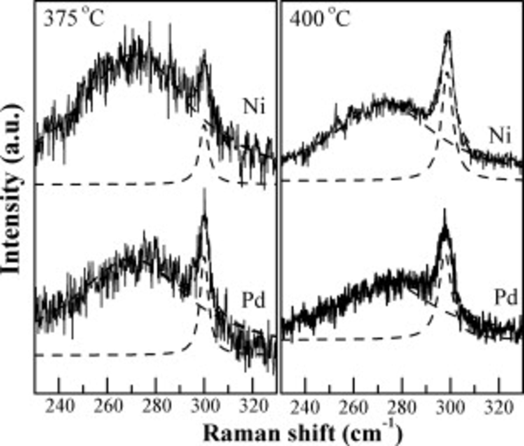
Figure 8. Raman scattering spectra measured on MILC/amorphous interface of Ge (Ni) and Ge (Pd) samples annealed at 375 and  .
.
Table III. Tensile strain in MIC and MILC Ge annealed at 375 and  .
.  is the anneal temperature and
  .
.
 (°C) (°C) | MIC | MILC | ||||
|---|---|---|---|---|---|---|
| Co | Pd | Ni | Pd | Ni | ||
| 375 | ω 
| 297.9 | 297.7 | 297.6 | 300.1 | 300.0 |
| ε∥ (%) | 0.63 | 0.67 | 0.70 | 0.10 | 0.12 | |
| 400 | ω 
| 296.8 | 297.1 | 297.0 | 297.8 | 298.7 |
| ε∥ (%) | 0.89 | 0.82 | 0.84 | 0.65 | 0.43 | |
AFM was used to measure the surface roughness of MIC, MILC, and amorphous regions of Ge samples annealed at  . The scan area was
  , covering both MIC and MILC regions, from which their root-mean-square (rms) roughnesses were calculated from
  selections. For each data point, three-scans were performed at different locations, and their average was calculated. It can be seen in Fig. 9 that the rms roughnesses of the MILC regions are smaller than those of the MIC regions. Looking at the Ge MIC regions, there seems to be a correlation between surface roughness and Raman peak fwhm: the region with a sharper peak has a smaller surface roughness. The surface of the MIC region of the Ge (Co) sample is as smooth as that of deposited a-Ge.
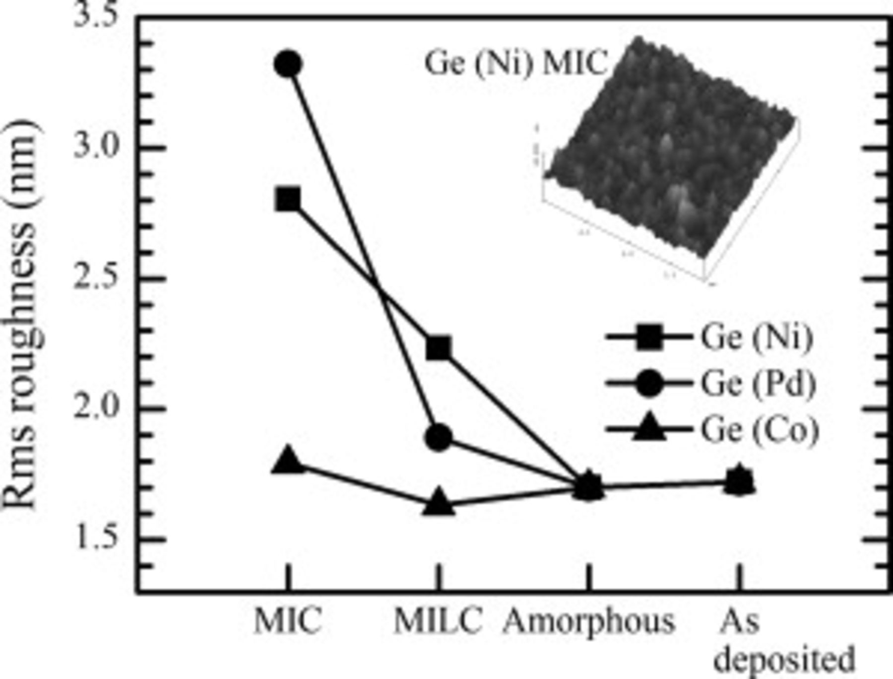
Figure 9. RMS surface roughnesses (measured by AFM) of MIC, MILC, and amorphous regions of Ge samples annealed at  and as-deposited a-Ge before anneal.
Conclusions
We have performed low temperature (from  ) MILC of Ge using Ni, Co, and Pd as metal seed, and compared the qualities of the crystallized Ge films and the lateral growth rates for each seed metal at different anneal temperatures. The lateral growth length and Ge quality are optimized when annealed at
  , higher than at which the lateral growth slows down (as observed in Ni and Pd samples) or even stops (in Co samples) due to self-nucleation of Ge. At the optimal anneal temperature of
  , the MILC rate in Ge (Ni) and Ge (Pd) are similar, and both are more than two times faster than Ge (Co)'s MILC rate. Although the Ge (Co) sample has a slow lateral growth, its MIC region has a high quality c-Ge film with small surface roughness. The slower lateral growth in Co samples is due to the smaller rate of metal alloy formation and diffusion, while the better crystalline quality is due to the small lattice mismatch of only 0.2% between Ge and
  . The MILC growth rate and the crystal quality of the MIC and MILC layers may not be related, as shown in Ge (Co) annealed at
  . As such, the choice of metal to be used in the MILC process depends on its application, whether it requires a longer crystal length with medium quality or whether it requires a high quality MIC film in which lateral growth length is not so crucial.