
Abstract
We report on the fabrication of ultraviolet (UV)-detecting  -based thin-film transistors (TFTs) and their isolation by energetic B ions. After deposition on a
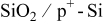 substrate at
 by radio frequency (rf) sputtering, the
 layer was patterned with Al source/drain (S/D) contacts and a
 window. Then energetic B ions with 30 and
 were implanted onto the deposited structures for device isolation. Among the three samples of unimplanted,
 -, and
 -implanted devices, the
 -implanted one displayed the least gate current leakage
 . The
 -TFT isolated with
 B also showed a field mobility of
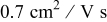 and on/off current ratio of more than
 , respectively. Under
 UV light of
 and at zero volts of gate bias, the device exhibited a photo-to-dark current ratio of
 with a temporal response of about
 .
Access this article
The computer you are using is not registered by an institution with a subscription to this article. Please choose one of the options below.
Purchase from
Purchase this article from our trusted document delivery partners.

Make a recommendation
To gain access to this content, please complete the Recommendation Form and we will follow up with your librarian or Institution on your behalf.
For corporate researchers we can also follow up directly with your R&D manager, or the information management contact at your company. Institutional subscribers have access to the current volume, plus a 10-year back file (where available).
