
Abstract
The electrical and optical properties of p‐type Ge and Si‐doped  layers grown by liquid phase epitaxy in an He ambient have been investigated as a function of the atom fraction of Si in the melt,
 . For
 in the range
 to
 the hole concentration at room temperature is relatively unaffected while the hole mobility decreases monotonically with addition of Si, suggesting close compensation of Si species. As a result, in the low temperature photoluminescent spectra, the pair transition via the shallow Si acceptors is quenched relative to that via the deep
 centers. For
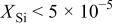 , adding 0.9 ppm
 to the growth ambient decreases the compensation due to the removal of the background S donor, and thereby increases the hole concentration by a factor of 2–3 and enhances the pair transition via the Si acceptors as well. The addition of
 during LPE growth is not, however, always practical as it has been found to affect the uniformity of thin epitaxial layers.
Access this article
The computer you are using is not registered by an institution with a subscription to this article. Please choose one of the options below.
Purchase from
Purchase this article from our trusted document delivery partners.

Make a recommendation
To gain access to this content, please complete the Recommendation Form and we will follow up with your librarian or Institution on your behalf.
For corporate researchers we can also follow up directly with your R&D manager, or the information management contact at your company. Institutional subscribers have access to the current volume, plus a 10-year back file (where available).
