
Abstract
Epitaxial layers were grown on semi‐insulating LEC  substrates by the chloride CVD technique and depletion type MESFET's with a gate length of 0.5 ̈m have been fabricated on these epitaxial layers. Correlation between the FET device performance and the substrate quality has been studied. It was found that the substrate quality largely affects the device performance. Dislocations of the substrate had no definite effect on the device performance, while the density of the precipitate‐like microscopic defects revealed by AB solution had a decisive effect on the device performance and the uniformity. We have examined LEC
 substrates with various density of etch pits revealed by AB solution (AB‐EPD) but with nearly the same order of dislocation density revealed by
 etching. The AB‐EPD ranged from less than 104 to
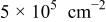 , while the average dislocation density was in the range of
 . The standard deviation of the
 compression over 2 in. ∅ wafers was very small in the case of low AB‐EPD wafers, while it was very large in the case of high AB‐EPD wafers. When the substrate with FETs was etched by AB solution after the device performance measurement, it became evident that FETs with several AB etch pits under the gate area exhibited lower performance. It was also found that the photoluminescence intensity and its distribution over the substrate corresponded with the etch pit pattern generated by the AB solution.
Access this article
The computer you are using is not registered by an institution with a subscription to this article. Please choose one of the options below.
Purchase from
Purchase this article from our trusted document delivery partners.

Make a recommendation
To gain access to this content, please complete the Recommendation Form and we will follow up with your librarian or Institution on your behalf.
For corporate researchers we can also follow up directly with your R&D manager, or the information management contact at your company. Institutional subscribers have access to the current volume, plus a 10-year back file (where available).
