
Abstract
The frequency of vanadium dioxide (VO2) oscillators is a fundamental figure of merit for the realization of neuromorphic circuits called oscillatory neural networks (ONNs) since the high frequency of oscillators ensures low-power consuming, real-time computing ONNs. In this study, we perform electrothermal 3D technology computer-aided design (TCAD) simulations of a VO2 relaxation oscillator. We find that there exists an upper limit to its operating frequency, where such a limit is not predicted from a purely circuital model of the VO2 oscillator. We investigate the intrinsic physical mechanisms that give rise to this upper limit. Our TCAD simulations show that it arises a dependence on the frequency of the points of the curve current versus voltage across the VO2 device corresponding to the insulator-to-metal transition (IMT) and metal-to-insulator transition (MIT) during oscillation, below some threshold values of  . This implies that the condition for the self-oscillatory regime may be satisfied by a given load-line in the low-frequency range but no longer at higher frequencies, with consequent suppression of oscillations. We note that this variation of the IMT/MIT points below some threshold values of
  is due to a combination of different factors: intermediate resistive states achievable by VO2 channel and the interplay between frequency and heat transfer rate. Although the upper limit on the frequency that we extract is linked to the specific VO2 device we simulate, our findings apply qualitatively to any VO2 oscillator. Overall, our study elucidates the link between electrical and thermal behavior in VO2 devices that sets a constraint on the upper values of the operating frequency of any VO2 oscillator.
Export citation and abstract BibTeX RIS

Original content from this work may be used under the terms of the Creative Commons Attribution 4.0 license. Any further distribution of this work must maintain attribution to the author(s) and the title of the work, journal citation and DOI.
1. Introduction
Memristors are emerging electronic devices with, usually, a simple and compact architecture made of an active layer and two electrodes. Their channel conductance can be programmed into two or more conductance states by triggering with an external stimulus. This resistive switching (RS) makes these devices ideal candidates to fabricate the elemental bricks of neuromorphic circuits, neurons or synapses, respectively, depending on whether RS is volatile or not. Recently, among the many possible physical mechanisms that give rise to RS, the insulator-to-metal transition (IMT) has attracted huge interest. IMT occurs in transition-metal oxides (TMOs), such as VO2 or NbO2. TMOs should behave like metals since they possess partially filled (3d, 4d or 4f) orbitals that are expected to give rise to a conductive band of electronic states. However, these materials are insulators since the incomplete band is indeed split into an empty and a filled band. Most importantly, the physical properties of TMOs may vary abruptly under the influence of external excitation. In this respect, VO2 exhibits a steep RS due to the change from insulating monoclinic (M1) to metallic tetragonal rutile-like (R) crystal structure. The IMT M1
 R is driven by temperature and occurs at a threshold temperature
  of about 340 K. The reverse metal-to-insulator transition (MIT) R
  M1 occurs during cooling down of the material, when a threshold temperature
  is achieved. Generally,
  is smaller than
  . Thus, the experimental curve of resistance R against temperature T shows hysteresis.
RS is also induced in VO2 when the latter is the channel of a two-terminal device, by applying voltage or injecting current across the channel. In this case, experimental evidence supports the idea that the driving mechanism is self-heating [2–5]. The channel of VO2 devices switches from an high resistance state (HRS) to a low resistance state (LRS) depending on the VO2 temperature, which is modulated by the Joule effect. The RS is volatile since the resetting to the original HRS occurs spontaneously upon a decrease in electrical power, which induces cooling down of VO2. Consequently, VO2 devices are named volatile Mott memristors [6–9].
A relaxation oscillator, which generates a non-sinusoidal periodic waveform at its output, can be obtained by connecting in series a VO2 volatile memristor with an RC parallel circuit [7, 10] (figure 1(e)). The self-oscillatory behavior at the output node of the oscillator circuit arises from cyclic charging and discharging of the external capacitor  , where these cycles are self-piloted by the VO2 volatile memristor being periodically in the ON/OFF (LRS/HRS) state. We define (
 ,
,  ) to be the IMT point of the curve current (I) versus voltage across the VO2 device (VD
), which is the point of the curve where the IMT occurs. Similarly, (
) to be the IMT point of the curve current (I) versus voltage across the VO2 device (VD
), which is the point of the curve where the IMT occurs. Similarly, ( ,
,  ) is the MIT point of the I–VD
curve where the MIT occurs. Then, the condition for the self-oscillatory regime is that the fixed oscillator circuit parameters, applied bias
) is the MIT point of the I–VD
curve where the MIT occurs. Then, the condition for the self-oscillatory regime is that the fixed oscillator circuit parameters, applied bias  and external resistance
  , are such that the load-line current (
 ) is larger than the
  at
at  , and smaller than
  at
at  . It is important to observe that VO2 oscillators are quite compact, which is an advantage for the scaling up of circuits with oscillators, considering that CMOS-based oscillators are realized with up to tens of transistors.

Figure 1. (a)–(c) TCAD model of steady-state resistivity  for temperature-triggered RS of a VO2 volatile memristor. (a) Material is in a high resistance state (HRS) below threshold temperature
  (about 340 (K)). Then, the IMT transition occurs, and the material switches to a low resistance state (LRS). Effect is volatile: the material resets to the original HRS if it is cooled down, usually below different threshold temperature
  . In the latter case, the curve
  versus T shows an hysteresis window. If the IMT is not so abrupt, then it will occur within an interval of temperatures
  . (b) During IMT (
 ) the temperature should always be increasing. If, instead, at a given moment, the material starts to cool, then
  remains constant, until the branch of the cooling cycle is reached. (c) During MIT (
 ) the temperature should always be decreasing. If, instead, at a given moment the material starts to warm, then
  remains constant, until the branch of the heating cycle is reached. This behavior emulates the observed experimental behavior of R versus T in VO2 [1]. (d) Crossbar (CB) architecture of a VO2 volatile memristor. (e) Schematics of a VO2 oscillator circuit. I, IL
and IC
are the currents across the VO2 device,
remains constant, until the branch of the heating cycle is reached. This behavior emulates the observed experimental behavior of R versus T in VO2 [1]. (d) Crossbar (CB) architecture of a VO2 volatile memristor. (e) Schematics of a VO2 oscillator circuit. I, IL
and IC
are the currents across the VO2 device,  and
and  , respectively. Representative, non-sinusoidal waveform of voltage at the output node over one period is also shown. (f) Self-oscillatory electrical behavior is associated with the compliance of the load-line with the self-oscillatory regime.
Download figure:
Standard image High-resolution imageRecently, oscillatory neural networks (ONNs) based on VO2 oscillators have been under intense scrutiny [10–12] as neuromorphic computing engines. Neuromorphic computing is an emerging discipline that aims to mimic highly efficient, brain-inspired computing strategies. There are different approaches to imitating brain activity. The mainstream implementation of neuromorphic circuits is through artificial neural networks [13]. In these systems, artificial neurons accumulate weighted input values, and the output is generated from the inputs through the application of an activation function. In spiking neural networks [14] the information is transmitted at the end of each cycle only at a given threshold. This closely imitates natural neurons, which fire when their membrane potential reaches a threshold, sending a signal to neighboring neurons. A third approach is represented by ONNs [15], which are systems of coupled oscillators that have been demonstrated to be powerful computing engines to emulate some brain functionalities [16–20].
ONNs encode information into the stable phase difference between each oscillator of the network and a reference oscillator, achieved if/when the system settles into a synchronized state [21, 22]. The energy that the ONN takes to compute is proportional to the ONN settling time [23], which is the number of cycles to synchronize multiplied by the oscillation period. The increase in oscillator frequency should bring about an overall reduction in energy consumption for ONN operativity. Thus, it is of interest for ONN applications to explore the range of frequencies at which oscillators can operate. Specifically, given the electrothermal mechanism driving the RS of VO2 volatile memristors, it can be expected that not only the electrical time constant, but also the thermal time constant plays a role in determining the oscillation period.
In this study, we perform electrothermal 3D technology computer-aided design (TCAD) mixed-mode simulations of a VO2 oscillator. We find that there exists an upper limit to its operating frequency, where this limit is not predicted from a purely circuital model of the VO2 oscillator. We investigate the intrinsic physical mechanisms that give rise to this upper limit. Our TCAD simulations show that the IMT/MIT points of current versus voltage across the VO2 device starts to depend on frequency, during oscillation, below some threshold values of  . This implies that the condition for the self-oscillatory regime may be satisfied by a given load-line in the low-frequency range but no longer at higher frequencies, with consequent suppression of oscillations. We find that this variation of the IMT/MIT points is due to a combination of different factors: 1) intermediate resistive states of VO2 achieved below some threshold values of
  that make HRS conductance of VO2 channel variable with frequency and 2) interplay between frequency and heat transfer rate. Although the upper limit on the frequency that we extract is linked to the specific VO2 device we simulate, our findings apply qualitatively to any VO2 oscillator. Overall, this study elucidates the link between electrical and thermal behavior in VO2 devices that sets a constraint on the upper values of the frequency of a VO2 oscillator.
2. TCAD simulation approach for VO2 volatile memristors and oscillators
We use finite element analysis (FEA) to solve the partial differential equations (PDEs) that model the device physics. In particular, we use the commercial Silvaco TCAD software suite to perform FEA calculations. This facilitates the implementation of multi-physics simulations, with many easily accessible built-in models of physical phenomena that can be integrated into a single simulation flow. We simulate VO2 volatile memristors with so-called crossbar (CB) geometry (figure 1(d)). These devices have been recently investigated since they show enhanced reliability and repeatability [11]. In FEA, the simulation domain (device architecture) has to be split into a discrete number of elements, whose ensemble is called a mesh, where the PDEs are numerically solved. In the present case, the VO2 device configuration is 3D and cannot be straightforwardly reduced to a 2D or 1D geometry. In addition, it is well known that 1D or 2D approximation of heat transfer analysis for a 3D problem may introduce errors (see for instance Kamala and Goldak [24]). Thus, we build a 3D mesh using Silvaco Victory Mesh [25] to reproduce the CB geometry. In this way, the coupled electrothermal behavior inside the VO2 channel is mimicked with a good approximation, which plays a key role in modulating the behavior of VO2 volatile memristors and oscillators [26–28].
We use Silvaco Victory Device [29] to solve PDEs of VO2 device physics on the generated mesh. We consider VO2 as a conductor, and we use a customized C-Interpreter function [26–28] of the PCM model [29] to empirically emulate VO2 resistivity. Overall, VO2 resistivity depends on local temperature T and time t after the Johnson–Mehl–Avrami model [30–32]:

where t is time,  is the time step, T is the local temperature,
  is the steady-state resistivity and τ is a lifetime. We calibrate the steady-state resistivity
  versus T (figure 1(a)) using experimental data of resistance
  versus temperature T [26]. Further details on the VO2 resistivity model and the calibration procedure are contained in appendix
Since VO2 is described as a conductor, the current density is  , for E the electric field and φ the electric potential. Thus, to calculate self-consistently the current transport and temperature distribution inside the VO2 volatile memristor we need to solve the Poisson equation coupled to the heat flow equation:

where K = 0.06 W (cm K)−1 [33] is the thermal conductivity, and C = 3 J (cm3 K)−1 [34] is the heat capacity per unit volume of VO2, respectively. The term  corresponds to the heat generation rate
  due to the Joule effect. For simplicity, we consider the bottom surface of the VO2 device as the only thermal contact (boundary). Therein, we specify the thermal boundary condition for the solution of (2) by setting that the projection of the energy flux, onto the unit normal, external to the boundary surface is
 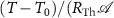 ), for T0 the external temperature,
  the interface thermal resistance and
  the bottom surface area of the device. The term
  ) regulates the heat dissipation of the VO2 volatile memristor with respect to the environment. Finally, we perform simulations of the VO2 relaxation oscillator by combining the TCAD engine to solve the PDEs of the VO2 device with a circuit solver (the so-called TCAD mixed mode), in such a way that the device physics is self-consistently solved at each iteration of the solver of the circuit equations.
3. Relationship between RS and oscillator frequency
We perform electrothermal 3D TCAD mixed-mode simulations of a VO2 oscillator (circuit scheme in figure 1(e)), where the VO2 CB device is made of an 80 nm thick VO2 layer inserted between the top and bottom Pt electrodes. The electrodes are 250 nm wide, while the VO2 layer is a square with each side 1 µm long. We set  K and
K and  K W−1 as boundary conditions at the thermal contact. We choose the circuit load-line specified by V
 2 V, R
 15 kΩ in order to comply with the self-oscillatory regime. We modulate the operational oscillator frequency by varying
  in the interval 5 nF–400 pF. The simulated voltages at the output node
  are shown in figure 2(a). The oscillations are turned-off at
  400 pF. Frequency versus
  of TCAD simulated oscillations are plotted (blue diamonds) in figure 2(b) and reported in table D3 in appendix
  and
and  , respectively (see appendix
  the simulated and the theoretically calculated data are almost overlapping. However, the theoretical calculations predict frequencies corresponding to
  values equal to or below 400 pF, while we are not able to obtain oscillations in this range of
  values. Thus, an upper limit to the achievable frequencies is not explained within the framework of a theoretical, purely circuital model of the VO2 oscillator (appendix

Figure 2. (a) Electrothermal 3D TCAD mixed-mode simulations of voltages at the output node  for
for  in the interval 5 nF–400 pF. Intrinsic device capacitance is accurately considered by simulation of device electrostatics. Parameters of circuit load-line: V
 2 V, R
 15 kΩ. (b) Frequency versus
  . Blue-diamond curve is from electrothermal 3D TCAD mixed-mode simulated oscillations. In this case, the frequency of oscillations ranges from 41.7 kHz (
 5 nF) up to 221.4 kHz (
 500 pF). At 400 pF the oscillations are inhibited. Red-asterisk curve is obtained by theoretical calculation through a purely circuital model of the VO2 oscillator where the VO2 device is simplified as a two-state VO2 variable resistor whose RS is activated by threshold voltages
  /
/ (appendix
  values are predicted well below 400 pF.
Download figure:
Standard image High-resolution imageIn figure 3(a), we plot curves I versus  (symbols) as extracted from simulated oscillations for
  10 nF, 5 nF, 1 nF, 800 pF, 500 pF and 400 pF. The circuit load-line is also drawn (dashed black line). It can be seen that up to a certain frequency (
 5 nF) all the curves essentially overlap, and then some mismatch becomes evident at higher-frequency values (lower
  values). In particular,
- 1.the IMT/MIT points become dependent from
 below some threshold value ( 800 pF for IMT points, 1 nF for MIT points); see insets of figure 3(a),
 - 2.the HRS branch of the I– curve is also dependent from for 1 nF.


Figure 3. (a) Curves of I versus  (symbols) as extracted from simulated oscillations (10 nF–400 pF). For comparison, quasi-static I versus
  (azure thick line) is also shown. Details about simulation of quasi-static I versus
  are reported in appendix
  (azure thick line) and T versus
  from simulated oscillations (symbols). In both panels (a) and (b) the HRS/LRS branches are highlighted.
Download figure:
Standard image High-resolution imageWe compare the above curves with the quasi-static I– (azure thick line of figure 3(a)). The curve is obtained by electrothermal 3D TCAD simulation of a voltage-controlled VO2 volatile memristor, where the VO2 device is connected in series with an external resistance of 1 kΩ, and the voltage sweeping rate is such to guarantee quasi-static conditions (see appendix
  are the same in quasi-static conditions and during oscillations up to when a dependence on
  arises of I–
 curves. This dependence on
  of IMT/MIT points implies an apparent modulation of the negative differential resistance (NDR) region with frequency. Indeed, the NDR region of a volatile memristor is rigorously defined from its DC current–voltage characteristics [36]. In our case, since the quasi-static I-
 and the DC I-
 overlap (as demonstrated in figure C2(b) in appendix
  in figure 3(a) is a rigorous reference. It should be observed that the value of current at the IMT point,
  , increases with frequency for
  800 pF, while the value of current at the MIT point,
  , decreases with frequency for
  1 nF. Since the load-line current is independent of
  , then it may be expected that it will become smaller than the
  at
at  , and/or larger than the
  at
at  for a certain value of
  . This will make the load-line no longer compliant with the conditions for a self-oscillatory regime, which explains our observation of inhibition of self-oscillations at certain frequencies.
To understand better the upper limit to the frequency of a VO2 oscillator, we need to investigate the mechanism of variation of the IMT/MIT points, and of the HRS branch of I– , above threshold frequencies. From the electrothermal 3D TCAD mixed-mode simulated oscillations, we extract the local temperature as probed in the geometrical center of the device, T. We consider it as a good descriptor of the temperature of the 'channel', given that the temperature is approximately uniform therein [26, 28]. We plot in figure 3(b) the curves (symbols) of T vs
  for
for  10 nF, 5 nF, 1 nF, 800 pF, 500 pF and 400 pF. We also extract from the electrothermal 3D TCAD simulations of quasi-static I–
 the associated T–
 (azure thick line in figure 3(b)). It can be seen that:
- 3.the temperatures, associated with IMT points, become dependent on for 800 pF, while the temperatures , associated with MIT points, are constant and equal to 320 K.


In particular, the points ( ,
,  ) appear (approximately) located along the part of quasi-static T–V
 corresponding to HRS-to-LRS transition (dashed red line). In the case of
  400 pF, T is constant, with a value slightly below the HRS-to-LRS branch of quasi-static T–V
 . Thus, T does not achieve the value for RS at
  400 pF, which is consistent with the suppression of oscillations in this case.
In figure 4(a), it is shown the plot of T against time normalized to the oscillation period ( ) for an oscillation cycle, where
  10 nF, 5 nF, 1 nF, 800 pF, 500 pF and 400 pF. The use of
  allows to compare the temperature profiles during oscillations at different frequencies. In figure 4(b), the corresponding local resistivity as probed in the geometrical center of the device (ρ) is plotted against
  for an oscillation cycle. The T versus
  (and ρ versus
  ) curves show dependency on frequency for
  1 nF, even though the qualitative behavior is the same. Finally, figure 4(c) reports the plot of ρ versus T during an oscillation cycle.

Figure 4. (a) T versus  (b) ρ vs
  and (c) ρ versus T for an oscillation cycle.
  10 nF–400 pF. Red crosses represent the points at the beginning of
  discharging, after MIT. From panels (a) and (c) it can be seen that these points are associated with
  sign flipping during LRS-to-HRS transition. From panels (b) and (c) it can be seen that the sign flipping occurs before the HRS heating branch is recovered. This makes accessible intermediate HRS values of resistivities, until the HRS heating branch is intercepted (gray circles) and the quasi-static HRS resistivity is recovered. If the HRS heating branch is not intercepted before HRS-to-LRS transition, the intermediate values of resistivities determine the IMT points, making them frequency-dependent.
Download figure:
Standard image High-resolution imageFigure 4(a) shows that the temperature increases abruptly to the maximum  value very shortly after the IMT point, which is consistent with a sharp increase in the current due to IMT. This value is well above the temperature needed to complete the transition to the metallic state, thus ρ becomes equal to
  (which, for simplicity, we have assumed to be constant, see table B2 in appendix
  that in contrast is kept constant. Instead, it is due to the change (decrease) in electrical power (the heat source) after IMT switching.
The resetting to the HRS state occurs at the MIT point, and starts the discharging of the external capacitor. Overall, figure 4(c) shows that ρ at the beginning of discharging has not recovered the frequency-independent values of the HRS heating branch (figure B1(b) in appendix  1 nF, it always recovers the HRS heating branch during the heating cycle (gray circles in figures 4(b) and (c)), before the HRS-to-LRS transition. This explains why IMT points do not depend on
  up to
up to  1 nF. For
  1 nF, ρ at the beginning of discharging has the same value of
  of quasi-static I–
 . This value is retained during the entire heating cycle and the HRS heating branch is intercepted just at the IMT point. This explains why the IMT points are the same, although the HRS part of I–
 differs from the one of the quasi-static I–
 . Finally, for
  800 pF, the value of ρ at the beginning of discharging is smaller than
  . Thus, the HRS heating branch is never recovered, and not both the HRS part of I–
 and also the IMT point start to depend on
  .
.
The above-described behavior is clarified by observing the ρ versus T during oscillations in figure 4(c). The ρ values at the beginning of discharging (red crosses in figures 4(b) and (c)) correspond to the ones where the temperature trend switches from decreasing to increasing (sign flipping of  ; red crosses in figures 4(a) and (c)). Since this occurs before the transition to the insulating state is completed, the TCAD ρ value is frozen at an intermediate resistivity value until when/if the HRS heating branch of ρ (figure B1(b) in appendix
The above discussion demonstrates the key role played by the change of T versus t with frequency. Thus, we need to look at the variation of  with frequency. In principle, the temporal derivative of T can be calculated directly from T versus t of simulated oscillations. However, we can also approximate it from the heat diffusion equation [37] as the sum of two components:

where P is the electrical power from simulated oscillations,  is the thermal capacity where
  is the volume of the CB device, A is the heat transfer surface area and
  is the average over A of the heat transfer coefficient [37]. Through equation (3), the t-behavior of T can be simply correlated with the electrical power and the heat transfer rate during the oscillation cycle. For the present device geometry (
 cm3) we calculate
  J K−1. We extract
  by following the approach used in [28]. We match the quasi-static simulated T to
  , where P is the quasi-static simulated power. We obtain that
  W K−1 (see appendix
  calculated from equation (3) with the temporal derivative determined directly from T versus t as obtained from simulated oscillations (figure F1 in appendix
Figure 5 shows the two components of equation (3) as plotted against  . It can be seen that both
  and
and  are almost unaffected up to
  5 nF, and then start to depend on frequency. In particular, we can distinguish between the charging or discharging parts of an oscillation cycle. During the charging part of the oscillation cycle (when VO2 is in the LRS), the term
  begins to depend on frequency for
  1 nF. In particular, the absolute value of
  increases with frequency for each value of
  when it is
  0.2 V. However, this is not due to the corresponding increase in
  , given that the latter is not dependent on
  . Indeed, this is consistent with the fact that
  with
with  is constant when VO2 is in the LRS (see table B2 in appendix
  means a decrease in thermal dissipation with consequent thermal build-up in this range of frequencies. This conclusion agrees with the thermal time constant of the oscillator estimated to be
  s, which thus becomes comparable to the period of charging (
 s) for
  500 pF. In this way, the temperature
  K is achieved at lower and lower power for
  1 nF, which explains the observed dependence on
  on
on  in this range. Regarding the discharging part of the oscillation cycle, it can be seen that the term proportional to P begins to depend on frequency for
  1 nF. This is consistent with the above observation that the HRS branch of I–
 varies with
  for
for  1 nF.
1 nF.

Figure 5. The two components of equation (3),  and
and  , plotted against
  . Red ellipses highlight the LRS part of the oscillation cycle where the increase in absolute value of
  is not correlated to an increase in
  , and thus it can only be explained as being due to a reduction in the efficiency of thermal dissipation in this range of frequencies.
Download figure:
Standard image High-resolution imageFinally, it is worth observing that, in principle, the modulation of IMT/MIT points from frequencies above a threshold value can be compensated by changing the load-line. Since the value of  decreases with frequency (
 1 nF) while the value of
  increases with it (
 800 pF), as a consequence, 'flatter' and 'flatter' load-lines are necessary to continue to comply with the self-oscillatory regime. This is shown in figure 6. Oscillatory behavior at
  400 and 350 pF is achieved with a load-line specified by V
 10 V, R
 80 kΩ. The corresponding oscillation frequencies are 294 kHz (
 400 pF) and 291 kHz (
 350 pF). Oscillatory behavior at
  320 pF is achieved with a load-line specified by V
 30 V, R
 240 kΩ, with a corresponding oscillation frequency of 283 kHz. Thus, the load-line parameters
  and
and  have to be increased more and more to maintain compliance with the self-oscillatory regime, with a not negligible cost in terms of power consumption. Finally, it becomes practically impossible to find a load-line yielding a self-oscillatory regime for
  300 pF and below.

Figure 6. Curves of I versus  (symbols) as extracted from simulated oscillations. Oscillatory behavior at
  500 pF corresponds to load-line specified by V
 2 V, R
 15 kΩ (black dashed line). Oscillatory behavior at
  400 and 350 pF is achieved with a load-line specified by V
 10 V, R
 80 kΩ (red line). Oscillatory behavior at
  320 pF is achieved with a load-line specified by V
 30 V, R
 240 kΩ (blue line). For comparison, quasi-static I versus
  (thick azure line) is also shown.
Download figure:
Standard image High-resolution image4. Conclusion
In this study, we use electrothermal 3D TCAD simulations to investigate the factors that may set an upper limit, if any, over the maximum frequency achievable by a given VO2 oscillator. Our TCAD simulations show that the IMT/MIT points of current versus voltage across the VO2 device depend on frequency, during oscillation, below some threshold values of  . This implies that the condition for the self-oscillatory regime may be satisfied by a given load-line in the low-frequency range, but no longer at higher frequencies, with consequent suppression of oscillations. It is important to observe that a theoretical, purely circuital model of the VO2 oscillator, where the VO2 device is simplified as a two-state VO2 variable resistor whose RS is activated by threshold voltages
  and
and  , respectively (appendix
Acknowledgments
Present address of S C: Silvaco France, 55 Rue Blaise Pascal, 38330 Montbonnot-Saint-Martin, France
S C and A T S conceived the idea. S C designed and performed the TCAD simulations. S C analyzed and validated the simulated data. S C, G B and A T S critically interpreted the data. A P and A N implemented the customized version of the PCM model used to simulate the VO2 material, and gave useful suggestions to implement TCAD simulations. S K supplied the experimental data used for the calibration of the TCAD model, and provided useful discussions to interpret them. All the authors discussed the results. S C drafted the manuscript and A T S critically revised it. The manuscript has been read and approved by all authors. A T S had the management, coordination responsibility and supervision for the planning and execution of the research activity leading to this publication. A T S acquired the financial support for the project leading to this publication.
This study was supported by the European Union's Horizon 2020 research and innovation programme, EU H2020 NEURONN (www.neuronn.eu) project under Grant No. 871501.
Data availability statement
The data that support the findings of this study are openly available at the following URL/DOI: https://osf.io/sw7va/.
Code availability statement
The input files to implement TCAD simulations with Silvaco Victory Mesh and Victory Device tools are provided as supporting material.
Appendix A: VO2 devices as memristive one-ports
VO2 is a thermistor material with a negative temperature coefficient, since it is a thermally sensitive resistor exhibiting a decrease in electrical resistance with an increase in its temperature. Noticeably, thermistor devices are among 'some examples of physical devices which should be modeled as memristive one-ports' [38]. The equations describing the system are as follows:

and the heat transfer equation,

provided that C is the heat capacitance, δ is the dissipation constant and P(T) is the electrical power. Equation (A.2) can indeed be rewritten as,

and the combination of (A.1) and (A.3) implies that a thermistor device is a first-order time-invariant current-controlled memristive one-port.
It is important to observe that the above description is an ideal 0D model, where indeed the whole channel is considered to be a homogeneous resistor dependent on the temperature T. This description would apply, rigorously, if the VO2 channel was self-heated homogeneously, which corresponds to the current flowing through the channel in a homogeneous way. This is not the case for a CB VO2 device, where just the part between overlapping top and bottom contacts is involved in device conduction, making it a true 3D physical system. Consequently, (A.1) and (A.3) appear in this study in their microscopic, local version as  and equation (2), respectively, with the functional form of
  given in appendix B.
Appendix B: TCAD resistivity model of VO2 and calibration procedure
In our TCAD approach, VO2 is considered to be a conductor, whose local resistivity depends on local temperature T and time t according to equation (1). In particular, the steady-state resistivity  is described by the set of equations listed in table B1. This set of equations apply for both (heating and cooling) branches of
  , where by a heating (or cooling) branch is meant the curve
  when the external temperature is increased (or decreased) monotonically. The temperature interval
  corresponds to the one of transition from HRS to LRS (for the heating branch), or of transition from LRS to HRS (for the cooling branch). The parameters
  ,
,  ,
,  ,
,  ,
,  ,
,  , are calibrated against available experimental measurements of resistance R versus temperature T (figure B1(a)) of a real CB device. The experimental data are obtained as follows. The VO2 resistance is measured in steady-state condition at different temperatures as provided by heating VO2 through an external heater, without any contribution to heat generation in the VO2 layer due to the Joule effect.

Figure B1. (a) Experimental resistance R versus temperature T data used for calibration of the resistivity model. (b) Calibrated TCAD  . Red solid line is the heating branch of the curve, corresponding to the variation of
  when T is monotonically increasing with time. Dotted blue line is the cooling branch of the curve, giving the variation of
  when T is monotonically decreasing with time. HRS/LRS parts of heating/cooling branches are highlighted.
Download figure:
Standard image High-resolution imageTable B1. Analytical expressions of heating/cooling branches of TCAD  .
.

| Condition |
|---|---|

| if 
|

| if 
|

| Otherwise |
The experimental device is made of a square VO2 layer with each side 5 µm and a thickness of 80 nm, while the width of the contacts is 250 nm. To perform the calibration, first we have to extract the resistivity from the experimental resistance. To do this, we use the formula  , where L is the 'channel' length (that is the VO2 thickness), and
  , for AC
the cross-sectional area of overlapping electrodes, and a is a parameter. We determine a by performing a voltage-controlled 3D electrothermal simulation of the VO2 device in series with an external resistor of 1 kΩ, and by fitting the HRS parts of 1) simulated I versus VD
and 2) experimental I–VD
. If the current flow is coincident with the region of overlapping between the two contacts, then it would be a = 1, while we find a = 2.7. Finally, the hysteresis of
, for AC
the cross-sectional area of overlapping electrodes, and a is a parameter. We determine a by performing a voltage-controlled 3D electrothermal simulation of the VO2 device in series with an external resistor of 1 kΩ, and by fitting the HRS parts of 1) simulated I versus VD
and 2) experimental I–VD
. If the current flow is coincident with the region of overlapping between the two contacts, then it would be a = 1, while we find a = 2.7. Finally, the hysteresis of  is implemented by using different parameters for the heating/cooling branches of
  . The calibrated parameters are shown in table B2.
Table B2. Calibrated parameters of TCAD  .
.

|

|

|

|

|

| |
|---|---|---|---|---|---|---|
| Branch | ( cm K)−1 cm K)−1
| (K) | ( cm) cm) | ( cm K)−1 cm K)−1
| (K) | ( cm) cm) |
| Heating |

| 327.6 |

| 0 | 340.9 |

|
| Cooling |

| 304.6 |

| 0 | 320 |

|
The plots of figures 1(b) and (c) schematize the capability of the TCAD model to reproduce the experimentally observed intermediate resistive states in R versus T curves obtained when the sweep of temperature is inverted before the full HRS-to-LRS transition (or the reverse) is completed [1]. The authors of [1] have found that if, at a given intermediate resistance value during the HRS-to-LRS transition, the trend of temperature values is inverted (so that it is no longer increasing), then the resistance remains approximately constant at such an intermediate value. The same applies if, at a given intermediate resistance value during the LRS-to-HRS transition, the trend of temperature values is inverted. In our TCAD model, this experimental behavior is implemented as follows: at each simulation time t step, the  is calculated at each mesh point for the local temperature T(t) at this point, and:
- I.during the heating cycle, if the current T(t) is no longer higher than the temperature at previous time step Told , then is frozen: .
- II.during the cooling cycle, if the current T(t) is no longer lower than the temperature at previous time step Told , then is frozen: .


Appendix C: Simulation of quasi-static I– and DC I–


The quasi-static I- (azure line of figure 3(a) and cyan lines of figure C1) has been simulated by sweeping an applied voltage of 0.5 V for a ramp time of 1.875 ms onwards (and sweeping backwards to 0 V in the same time interval), where the VO2 device is connected in series with an external resistance of 1 kΩ. Indeed, this setup corresponds to a quasi-static condition, as it is demonstrated by the fact that overlapping curves are obtained by applying the same voltage for ramptimes of 0.1875, 18.75, 187.5 ms and 1.875 s (black lines in figure C1(a)). The quasi-static condition does not apply any longer for shorter ramp times, as shown when the ramp time is 37.5 µs (orange triangles in figure C1(b)) or less. We have also simulated the current–voltage characteristic in DC mode. We have determined each point (I,
  ) of the DC curve by applying a bias that is constant with time. Whenever the bias is applied, the current starts to flow across the channel, and the Joule effect produces an increase in local temperature which, in turn, modifies the local resistivity. Thus, the system needs some time to achieve equilibrium. Figure C2(a) shows
  /max(
/max( ) versus time for any bias applied. It can be observed the change of
  with time, until an equilibrium state is achieved. In the inset, the equilibrium time is plotted, defined as the time necessary to achieve equilibrium, versus the applied bias. Overall, the DC current–voltage characteristics is obtained by repeating the simulations at different, constant applied bias. The DC I-
 is reported in figure C2(b) (star symbols). It can be seen that the quasi-static I-
 and the DC I-
 overlap. Thus, the NDR region determined from the quasi-static I-
 falls into the rigorous definition of the NDR region of a volatile memristor (see for instance [36]).

Figure C1.
I– obtained by sweeping an applied voltage of 0.5 V for different ramp times: (a) equal to or greater than 0.1875 ms, or (b) equal to or smaller than 37.5 µs. In both panels, the cyan line is the curve corresponding to a ramp time of 1.875 ms.
Download figure:
Standard image High-resolution image
Figure C2. (a)  /max(
/max( ) versus time for any bias applied. Change of
  with time is observed, until an equilibrium state is achieved. In the inset, the equilibrium time versus the applied bias is plotted, where the equilibrium time is the earliest time at which the
  values stabilize to fixed values. (b) DC I-
 (star symbols). Quasi-static I-
 , obtained by sweeping an applied voltage of 0.5 V along a ramp time of 1.875 ms onwards, and sweeping backwards to 0 V in the same time interval, is plotted for comparison. It can be seen that the quasi-static I-
 and the DC I-
 overlap.
Download figure:
Standard image High-resolution image
A final remark. We have derived resistance values  kΩ and
  from the quasi-static I–
 of VO2 memristor. We have used these values to approximate the memristor as a two-state variable resistor in the purely circuital model of the VO2 oscillator, which we have applied to calculate the theoretical frequencies (red asterisks) of figure 2(b) (appendix D).
Appendix D: Frequencies calculated by theoretical circuit model of the VO2 oscillator
Theoretical frequencies shown in figure 2(b) (red asterisks) are calculated through the purely circuital model of the VO2 oscillator where the VO2 volatile memristor is approximated as a two-state (LRS/HRS) variable resistor, activated by threshold voltages  and
and  , respectively. For generality, we consider the two possible topologies of the VO2 oscillator circuit, where
  is connected across
  (figure D1(a)), or across the VO2 device (figure D1(b)). The equivalent Thevenin circuit (figure D1(c)) is similar, since the equivalent Thevenin resistance is
  , while the equivalent Thevenin voltages are slightly different:


Figure D1. (a) and (b) are the two possible oscillator circuit topologies. In both cases, the blue part of the  waveform corresponds to cooling of the VO2 channel (VO2 is ON), the red part corresponds to heating of the VO2 channel (VO2 is OFF). (c) Equivalent Thevenin circuit.
Download figure:
Standard image High-resolution imagewith  ,
,  depending on whether the VO2 channel is in the ON, OFF state.
It should be observed that  is charging/discharging when VO2 is in the ON/OFF state, respectively, if circuit topology is the one shown in figure D1(a). The reverse applies, instead, if the circuit topology is the one shown in figure D1(b) (see, for instance [39]). Overall, the voltage transient at the output node is as follows:

with  .
.  is equal to
  for τ oscillation period, where
  .
.
The time of charging/discharging can be derived from (D.1) as,

and the period can be estimated as  , where
  is the time interval of
  charging and
  is the time interval of
  discharging.
This brings us to the following set of equations for the circuit topology of figure D1(a):


Thus,  for
for  .
.
For the circuit topology of figure D1(b):


Thus,  for
for  .
.
The theoretical frequencies plotted in figure 2(b) have been extracted from the periods  of VO2 oscillator with the circuit topology drawn in figure D1(a). They are listed in table D2. The parameters used to perform calculations are listed in table D1, with the following:
  1.572 632 678 8559 V,
  1.908 088 235 2941 V,
  1.712 915 98 V,
  1.881 303 54 V. We have calculated the theoretical frequencies extracted from the periods
  of the VO2 oscillator with the circuit topology drawn in figure D1(b). Indeed, we have found that
  , which means that the two circuit topologies yield the same period for any given
  value. The parameters used to perform these latter calculations are listed in table D1, with the following:
  0.427 367 321 144 V,
  0.091 911 764 7059 V,
  ,
,  .
.
Table D1. Parameters used to calculate theoretical frequencies.

|

|

|

|

|

|
|---|---|---|---|---|---|
| 4.0763 kΩ | 722.5434 Ω |
 V V |
 V V |
 kΩ kΩ |
 Ω Ω |
Table D2. Frequencies calculated by theoretical circuit model.
 (pF) (pF) | 104 |

| 103 | 800 | 600 | 500 | 400 | 300 |
|---|---|---|---|---|---|---|---|---|
| Frequency (kHz) | 25.7 | 51.3 | 256.6 | 320.8 | 427.7 | 513.2 | 641.6 | 855.4 |
 (pF) (pF) | 200 | 100 | 10 | |||||
| Frequency (kHz) | 1.283 
| 2.566 
| 2.566 
|
Table D3. TCAD Simulated Frequencies.
 (pF) (pF) | 104 |

| 103 | 800 | 600 | 500 |
|---|---|---|---|---|---|---|
| Frequency (kHz) | 21.6 | 41.678 | 157.9 | 182.935 | 210.2 | 221.4 |
Appendix E: Determination of

To determine  , we follow [28]. We match the temperature T, as probed in the center of the active region of the device, with
  , for P the device power. A is the heat transfer surface area and
  the heat transfer coefficient averaged over A [37]. Both T and P are extracted from TCAD 3D electrothermal simulation of quasi-static I versus
  . The use of
  is equivalent to modeling the heating effects in the VO2 device with the theory for thermistors [40]. We achieve an excellent agreement (figure E1) by
  W K−1.

Figure E1. TCAD-simulated local temperatures probed in the geometrical center of the device (solid lines) for T0 equal to 293 and 313 K, and temperatures calculated from  (symbols).
Download figure:
Standard image High-resolution imageAppendix F: Simulated and calculated


Figure F1. Temporal derivative of T determined by curve T versus t from simulated oscillations, and calculated from equation (3) of the manuscript, for  equal to (a) 10 nF, (b) 5 nF, (c) 1 nF, (d) 800 pF and (e) 500 pF. In each case, the match between the two curves is good overall, especially at lower frequencies. Discrepancies start to appear at higher frequencies (Cext below or equal 1 nF), especially in the LRS part of the oscillations.
Download figure:
Standard image High-resolution image
Supplementary data (0.3 MB PDF)