
Abstract
Topological-soliton-based devices, like the ferromagnetic domain-wall device, have been proposed as non-volatile memory (NVM) synapses in electronic crossbar arrays for fast and energy-efficient implementation of on-chip learning of neural networks (NN). High linearity and symmetry in the synaptic weight-update characteristic of the device (long-term potentiation (LTP) and long-term depression (LTD)) are important requirements to obtain high classification/regression accuracy in such an on-chip learning scheme. However, obtaining such linear and symmetric LTP and LTD characteristics in the ferromagnetic domain-wall device has remained a challenge. Here, we first carry out micromagnetic simulations of the device to show that the incorporation of defects at the edges of the device, with the defects having higher perpendicular magnetic anisotropy compared to the rest of the ferromagnetic layer, leads to massive improvement in the linearity and symmetry of the LTP and LTD characteristics of the device. This is because these defects act as pinning centres for the domain wall and prevent it from moving during the delay time between two consecutive programming current pulses, which is not the case when the device does not have defects. Next, we carry out system-level simulations of two crossbar arrays with synaptic characteristics of domain-wall synapse devices incorporated in them: one without such defects, and one with such defects. For on-chip learning of both long short-term memory networks (using a regression task) and fully connected NN (using a classification task), we show improved performance when the domain-wall synapse devices have defects at the edges. We also estimate the energy consumption in these synaptic devices and project their scaling, with respect to on-chip learning in corresponding crossbar arrays.
Export citation and abstract BibTeX RIS

Original content from this work may be used under the terms of the Creative Commons Attribution 4.0 license. Any further distribution of this work must maintain attribution to the author(s) and the title of the work, journal citation and DOI.
1. Introduction
1.1. Motivation
Among the various non Von Neumann/neuromorphic computing schemes recently proposed and implemented, crossbar arrays based on NVM devices as synapses can be deemed to be the most popular. These crossbar arrays carry out analog computing (both inference and training of neural networks (NN)) in analog memory systems (in-memory computing) very efficiently, both in terms of speed and energy [1–5]. During forward computation/inference, the crossbar array carries out vector-matrix multiplication (VMM) between the input vector and the synaptic weight matrix very fast by making use of Ohm's Law and Kirchoff's Current Law. During training of the NN (on-chip learning), the outer product operation between the input vector and the vector for common part of weight update at each output node can also happen inside the crossbar array. This enables parallel update of the synaptic weights of the crossbar array, and training of the crossbar array becomes efficient. In edge computing/edge artificial intelligence (AI), enabling on-chip learning at the edge devices prevents data breach, which can otherwise happen if edge devices only have inference facility [6–8]. Since on-chip learning in crossbar array is very efficient due to efficient VMM and outer product operations in it, on-chip learning in crossbar arrays becomes very attractive for edge AI applications [4, 6].
Some important functionalities that a NVM synapse device needs to exhibit to ensure accurate and efficient on-chip learning in a crossbar array made of such synapses are as follows [1, 3, 4]:
- (i)multiple conductance states.
- (ii)electrical read-out of these states.
- (iii)their electrical control in a linear and symmetric way between positive weight update (long-term potentiation, or LTP) and negative weight update (long-term depression, or LTD), while using programming pulses of identical magnitude and opposite polarity for LTP and LTD. Non-linearity and asymmetry have been found to degrade the classification accuracy of the neural network trained through on-chip learning [9]. Identical programming pulses are needed to make the peripheral circuit design simple.
- (iv)very high degree of non-volatility. After on-chip learning is achieved, the synaptic states of the trained network need to be retained over a long time for future testing/inference. One synaptic state cannot degrade into another, in the absence of programming pulses.
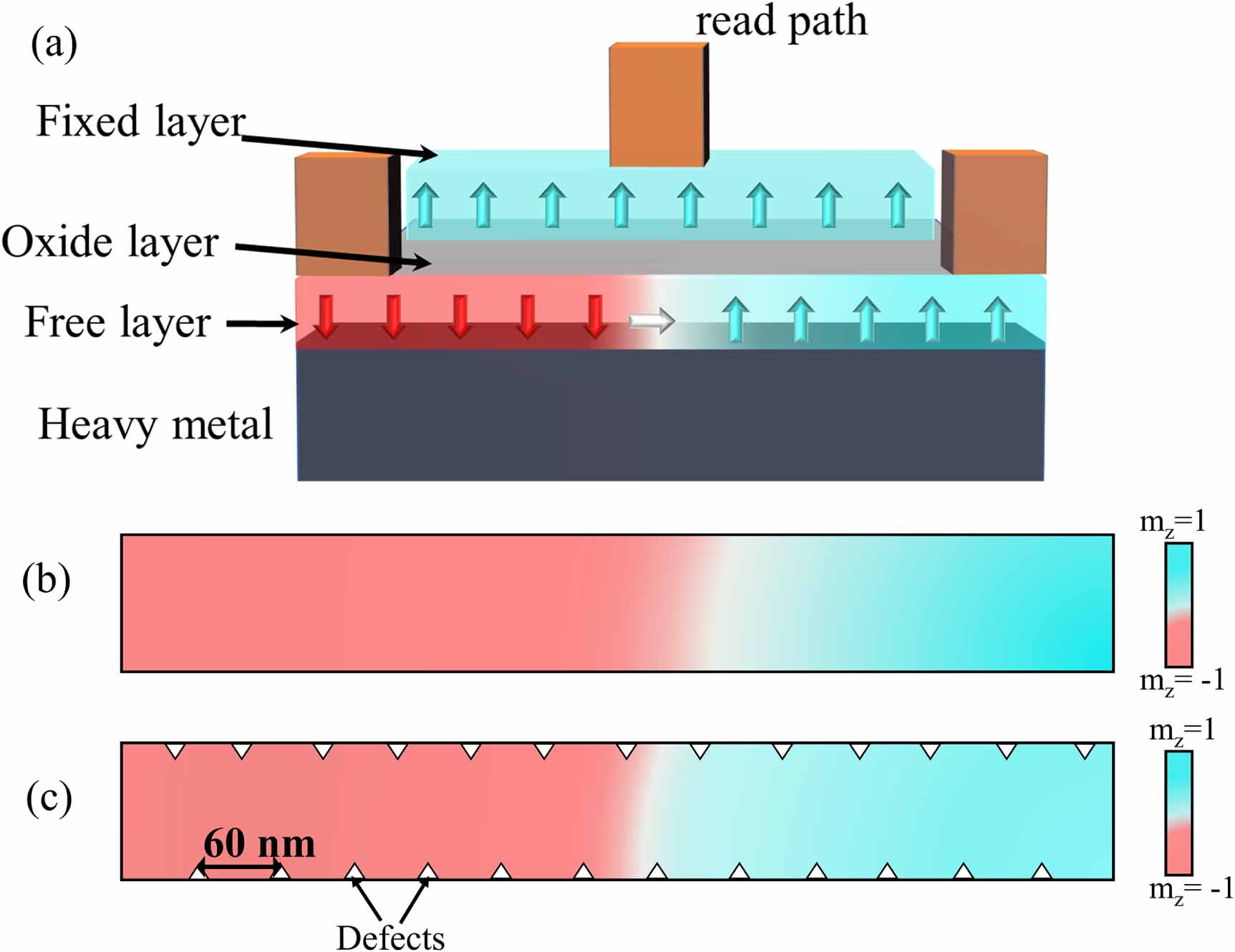
The domain wall is known to be a kink-like topological soliton [10–13]. In the heavy-metal-ferromagnetic metal (free layer)-oxide-ferromagnetic metal (fixed layer) device shown in figure 1(a), the ferromagnetic layer (free layer) exhibits perpendicular magnetic anisotropy (PMA), and the domain wall in that layer separates the region with up-polarized magnetic moments and that with down-polarized magnetic moments. In-plane current flowing through the heavy metal-ferromagnetic metal bilayer (figure 1(a)) has been shown, through simulations as well as experiments, to move the domain wall [14–20]. Different positions of the domain wall correspond to different proportions of up-polarized and down-polarized domains, and hence different values of average magnetization in the ferromagnetic layer. Because of the fixed-layer-oxide-free-layer-based magnetic tunnel junction (MTJ) structure present in the device (figure 1), different average magnetization values of the free ferromagnetic layer get translated to different conductance values through the tunnelling magneto-resistance effect (TMR) (more details on the operating physics of this device can be found in: [4, 21–25]. Thus requirements (i) and (ii) listed above are satisfied by this device. But for the domain-wall device to be used as NVM synapse in crossbar arrays in preference to other NVM synapse technologies like resistive RAM, phase change material, ferroelectrics, etc [1–4], it must satisfy all the four above criteria to a considerably better degree compared to these other technologies.

Figure 1. (a) Schematic of the domain-wall synapse device, showing the heavy metal layer, ferromagnetic free layer (in which the domain wall moves), oxide layer and fixed layer. (b) Schematic of the ferromagnetic free layer for the device without defects, red colour corresponds to magnetic moments pointing vertically down ( ) and blue colour corresponds to moments pointing up (
 ). (c) Schematic of the ferromagnetic free layer for the device with defects, which are essentially triangular regions with modified PMA (more details in the text).
Download figure:
Standard image High-resolution imageIt has already been shown through simulations and experiments (as mentioned earlier) that in-plane current pulses flowing through the device (shown in figure 1(a)) move the domain wall, and reversing polarity of the current reverses the direction of domain-wall motion. Thus electrical control of the conductance states through programming current pulses has already been shown in this device. However, achieving sufficient linearity and symmetry in the control, as required in requirement (iii) above, has remained a challenge experimentally. In this paper, we try to address this challenge by studying the impact of incorporation of defects at the edges of the domain-wall device on its synaptic characteristic. We also argue that the physical phenomenon behind the improvement of linearity and symmetry of LTP and LTD characteristics (requirement (iii)), which is pinning of the domain wall at defect sites, will lead to longer retention time of synaptic states (requirement (iv) above).
1.2. Related work
We briefly review the recent experimental reports on domain-wall devices next, with our focus being on the linearity and symmetry of the reported LTP and LTD characteristics (requirement (iii) above). Yadav et al [26] have recently quantitatively characterized the non-linearity and asymmetry of the experimentally obtained synaptic characteristic of a Co/Pt/SiO2-based domain-wall device (upon the application of identical pulses for LTP, and identical pulse streams for LTD) with the help of the method followed in the literature of the Neuro-Sim simulator [9, 27, 28], popularly used for this purpose across different NVM synapse technologies. They have reported non-linearity coefficient for LTP αP
= 3.875, non-linearity coefficient for LTD  , and thus asymmetry coefficient (
 ) = 7.715, for their device. While Zhang et al [29] have not quantitatively characterized their experimentally obtained synaptic characteristic in similar devices, based on their reported plots of LTP and LTD, the non-linearity and asymmetry coefficients in their devices look similar to that reported by Yadav et al.
Zhang et al have reported much more linear and symmetric LTP and LTD characteristics compared to that but have not used identical programming pulses [30]. Their pulses are of increasing magnitude instead [30]; this makes the corresponding peripheral circuit design for on-chip learning very difficult because based on what weight value a synapse is currently at, a different pulse needs to be applied in this case.
Leonard et al have only experimentally reported 3–5 synaptic conductance states in their device (20–30 states are observed in the other reports) [31]. So estimating non-linearity and asymmetry factors for Leonard et al's reported data is difficult. Kumar et al have recently reported synaptic behaviour in a similar domain-wall device through magneto-optic Kerr effect (MOKE) images and change in TMR of the MTJ structure due to current-driven domain-wall motion [32]. But they have not reported any LTP–LTD plot from which the non-linearity and asymmetry coefficients can be inferred.
1.3. Our contributions
In this context, we have made the following contributions through this paper (we also present the section organization here). In section 2, we show through micromagnetic simulations that the presence of defects at the edges of the device, with PMA constant in the defects higher than that in the rest of the ferromagnetic layer, improves the linearity and symmetry of the LTP and LTD characteristics of the device drastically (requirement (iii) above). This is because these defects act as pinning centres for the domain wall and prevent it from moving during the delay time between two consecutive programming current pulses (even under high thermal field), which is not the case when the device does not have defects. We also argue that this same physics of domain-wall pinning at defects improves the long-time synaptic state retention property (non-volatility) of these devices (requirement (iv) above).
It is to be noted that our method for pinning the domain wall is different from that reported by Liu et al [33] and Dhull et al [34]. In these other two reports, notches/grooves on the two edges of the magnetic layer which pin the domain wall are essentially regions where there is no magnetic material at all ( ). In our case, there is magnetic material inside the defects with the same Ms
value as rest of the layer but with a higher PMA value.
). In our case, there is magnetic material inside the defects with the same Ms
value as rest of the layer but with a higher PMA value.
In section 3, we incorporate the LTP and LTD characteristics from the micromagnetic model of the device (both for the case with defects and without defects) in system-level models of crossbar-array-based long short-term memory (LSTM) network [35] and fully connected neural network (FCNN) [36]. On-chip learning of the LSTM is carried out using a thresholded version of the back-propapagtion through time (BPTT) algorithm [35–38], while that of the FCNN is carried out using a thresholded version of the standard back-propagation algorithm [24, 36]. We show that both for LSTM and FCNN, on-chip learning performance (measured in terms of loss or classification accuracy) is much better in the case of devices with edge defects than without defects because of the improved linearity and symmetry (of LTP and LTD) due to these defects.
Our LSTM-related work mentioned above is important from another perspective as well, which is the following. Extensive designs and on-chip learning results have been shown for domain-wall-synapse-crossbar array-based feed-forward NN: the FCNN, with and without hidden layers, as well as the convolutional neural network (CNN) [23, 24, 31, 34, 39]. These networks are typically used for image classification problems (as we have shown here as well with the image set of handwritten digits: MNIST) [36, 40]. But to the best of our knowledge, not much work has been reported on recurrent neural networks (RNNs) based on domain-wall synapse devices, or other spintronic devices. RNNs are extremely useful for natural language processing, speech processing, and regression tasks like time-series data prediction. So it is important to study on-chip learning in RNNs made of domain-wall-synapse-based crossbars so that on-chip learning of RNNs can be enabled in edge devices [35, 36]. So, in this paper, we show the design of a special kind of RNN (LSTM) using crossbar arrays of domain-wall synapses. Unlike most other RNNs, LSTMs do not suffer from the vanishing gradient problem [35, 37, 38]. In this paper, we show on-chip learning performance of the domain-wall-synapse-based LSTM crossbar array through a regression task on a time-series data set: Airline Passenger Numbers (1949–1960) [35, 37, 41]. Although system-level simulation and experiments on RRAM-synapse-based LSTMs and other RNNs have been published before [35, 37], to the best of our knowledge, this is the first report on system-level simulation of a domain-wall-synapse-based LSTM network.
2. Micromaganetic simulation of the domain-wall synapse device in the absence and presence of edge defects
2.1. Simulation methodology and parameter values
The methodology for micromagnetic modeling of the spin-orbit-torque-driven ferromagnetic domain-wall device has been discussed in details in various reports published before on this area [4, 21–25, 34, 42–48]. Here, we briefly summarize that methodology and then go into the specifics of how we have incorporated defects in the ferromagnetic layer which contains the domain wall. Using GPU-accelerated numerical package 'mumax3' [49], we have modelled the domain-wall dynamics by numerically calculating the time dynamics of the magnetic moments of the ferromagnetic free layer (coupled to each other through dipole-dipole interaction and exchange interaction), under the influence of spin current generated from the heavy metal layer underneath the ferromagnetic layer (figure 1(a)).
When charge current from the programming pulse flows through the non-magnetic heavy metal layer, a spin current is generated inside it via the spin Hall effect [50–52]. Under the assumption that the thickness of the heavy metal layer is higher than the spin diffusion length inside the metal, spin current density is defined as  =
=  , where jc
is in-plane charge current density and θSH
is the spin Hall angle of the heavy metals. For our simulation of both the devices without defects and with defects, we consider θSH
= 0.1, corresponding to platinum (Pt), which has been used as the heavy metal in the recent experimental demonstrations of such domain-wall synapse by Yadav et al [26]. Yadav et al have, in fact, reported this value of spin Hall angle in Pt in the same report [26] by carrying out hysteresis-loop-shift measurement on their device (following the method described by Hu and Pai [53] and Pai et al [54]). Spin diffusion length in Pt has been found to be 3–4 nm [55, 56]. So, if the thickness of the Pt layer in our device is about 10 nm, the above relationship between spin current and charge current will be satisfied.
, where jc
is in-plane charge current density and θSH
is the spin Hall angle of the heavy metals. For our simulation of both the devices without defects and with defects, we consider θSH
= 0.1, corresponding to platinum (Pt), which has been used as the heavy metal in the recent experimental demonstrations of such domain-wall synapse by Yadav et al [26]. Yadav et al have, in fact, reported this value of spin Hall angle in Pt in the same report [26] by carrying out hysteresis-loop-shift measurement on their device (following the method described by Hu and Pai [53] and Pai et al [54]). Spin diffusion length in Pt has been found to be 3–4 nm [55, 56]. So, if the thickness of the Pt layer in our device is about 10 nm, the above relationship between spin current and charge current will be satisfied.
For the device without defects, throughout the ferromagnetic layer (1000 nm × 100 nm), we use the following parameters in our micromagnetic simulation: saturation magnetization (Ms
) =  A m−1, PMA constant (K) =
  J m−3, exchange-correlation constant (A) =
  J m−1, and damping factor α = 0.3. These parameters have also been chosen based on the report by Yadav et al, where most of these parameters have been measured experimentally using a Pt/Co/SiO2 device [26, 57]. For our device with defects here, we include triangular regions on either side of the 1000 nm × 100 nm ferromagnetic layer (as shown in figure 1(c)), where PMA constant (K) =
  J m−3 and the rest of the parameters (Ms
, A, α) have the same values as before. These triangular regions are the defects which act as domain-wall pinning centres. The depth of each triangular region is 5.6 nm, and the separation between two consecutive such regions on one side of the device is 60 nm. In the ferromagnetic region outside the triangular regions, all the micromagnetic simulation parameters (including PMA constant K) are the same as that in the ferromagnetic layer of the device without any triangular regions (defects) (figure 1(b)). This method of incorporating defects with modified PMA in the micromagnetic simulation has been used before in reports by Sampaio et al [58] and Saxena et al [59].
J m−3 and the rest of the parameters (Ms
, A, α) have the same values as before. These triangular regions are the defects which act as domain-wall pinning centres. The depth of each triangular region is 5.6 nm, and the separation between two consecutive such regions on one side of the device is 60 nm. In the ferromagnetic region outside the triangular regions, all the micromagnetic simulation parameters (including PMA constant K) are the same as that in the ferromagnetic layer of the device without any triangular regions (defects) (figure 1(b)). This method of incorporating defects with modified PMA in the micromagnetic simulation has been used before in reports by Sampaio et al [58] and Saxena et al [59].
2.2. Simulation results: synaptic characteristics
In both the devices, we have created the domain wall in the ferromagnetic layer near the right end of the device. Next, we have applied current pulses of current density  A cm−2 for the device without defects and
  A cm−2 for the device with defects, positive polarity (for both devices), and pulse width of 1 ns (for both devices) in the presence of a constant in-plane assisting field Hx
= 3000 G. After every pulse, a delay of 100 ns is provided (similar delay is provided in experiments as well between programming current pulse and read current pulse). Then the average magnetization of the ferromagnetic layer is measured and plotted in figure 2(a) for device without defects and that with defects. The position of the domain wall just after each pulse and that after the delay (just before the next pulse is applied) are shown for both devices in figures 3 and 4 respectively. It is observed that starting from the right end, the domain wall moves leftward leading to expansion of the domain with up-polarized moment (mz
= 1) and thereby an increase of the average mz
of the ferromagnetic layer (LTP: figure 2(a)). Once the domain wall has crossed the middle of the device after 20 positive pulses meant for LTP, negative pulses are applied of the same magnitude (current density
A cm−2 for the device with defects, positive polarity (for both devices), and pulse width of 1 ns (for both devices) in the presence of a constant in-plane assisting field Hx
= 3000 G. After every pulse, a delay of 100 ns is provided (similar delay is provided in experiments as well between programming current pulse and read current pulse). Then the average magnetization of the ferromagnetic layer is measured and plotted in figure 2(a) for device without defects and that with defects. The position of the domain wall just after each pulse and that after the delay (just before the next pulse is applied) are shown for both devices in figures 3 and 4 respectively. It is observed that starting from the right end, the domain wall moves leftward leading to expansion of the domain with up-polarized moment (mz
= 1) and thereby an increase of the average mz
of the ferromagnetic layer (LTP: figure 2(a)). Once the domain wall has crossed the middle of the device after 20 positive pulses meant for LTP, negative pulses are applied of the same magnitude (current density  A cm−2 for the device without defects, and
  A cm−2 for the device with defects) and same duration (pulse width: 1 ns, delay between pulses: 100 ns). Now, the domain wall moves from right to left now as shown in figures 3 and 4. This leads to reduction of the domain with up-polarized moment (mz
= 1) and thereby a decrease of average mz
(LTD: figure 2(a)).
A cm−2 for the device with defects) and same duration (pulse width: 1 ns, delay between pulses: 100 ns). Now, the domain wall moves from right to left now as shown in figures 3 and 4. This leads to reduction of the domain with up-polarized moment (mz
= 1) and thereby a decrease of average mz
(LTD: figure 2(a)).
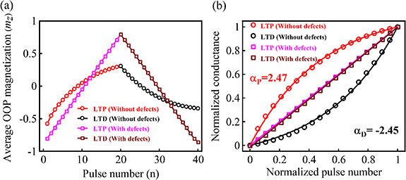
Figure 2. (a) Device without defects: for positive weight update/long-term potentiation or LTP (red plot), positive pulses of current density  A cm−2 have been applied in the presence of a 3000 G in-plane magnetic field. For negative weight update/long-term depression or LTD (black plot), 20 negative pulses of current density
  A cm−2 have been applied under the same 3000 G field. Both for LTP and LTD, each such programming current pulse is of 1 ns pulse width. We have allowed 100 ns delay between any two consecutive pulses. Device with defects: for positive weight update/LTP (pink plot), positive pulses of current density
  A cm−2 have been applied in the presence of a 3000 G in-plane magnetic field. For negative weight update/LTD (brown plot), 20 negative pulses of current density
  A cm−2 have been applied under the same 3000 G field. Same pulse width and delay between pulses are used as in (a). For both devices, average out-of-plane (OOP) magnetization (mz
) at the end of the delay is plotted as a function of pulse number. Thus, mz
here includes domain-wall motion both during the pulse and during the delay. (b) For non-linearity and asymmetry quantification of the device without defects, mz
in (a) is first converted to conductance (through TMR effect) and then normalized (minimum conductance = 0, maximum conductance = 1). Then, by fitting curves based on the equations provided with the NeuroSim simulator [9, 27, 28], the following numbers are obtained. Device without defects: non-linearity factor of LTP αp
= 2.47 (red plot), non-linearity factor of LTD
A cm−2 have been applied under the same 3000 G field. Same pulse width and delay between pulses are used as in (a). For both devices, average out-of-plane (OOP) magnetization (mz
) at the end of the delay is plotted as a function of pulse number. Thus, mz
here includes domain-wall motion both during the pulse and during the delay. (b) For non-linearity and asymmetry quantification of the device without defects, mz
in (a) is first converted to conductance (through TMR effect) and then normalized (minimum conductance = 0, maximum conductance = 1). Then, by fitting curves based on the equations provided with the NeuroSim simulator [9, 27, 28], the following numbers are obtained. Device without defects: non-linearity factor of LTP αp
= 2.47 (red plot), non-linearity factor of LTD  (black plot), and asymmetry =
  = 4.92. Device with defects: LTP (pink plot) and LTD (brown plot) curves are extremely linear, so the synaptic characteristic can be considered ideal with αp
= αd
= 0, and hence asymmetry also 0.
= 4.92. Device with defects: LTP (pink plot) and LTD (brown plot) curves are extremely linear, so the synaptic characteristic can be considered ideal with αp
= αd
= 0, and hence asymmetry also 0.
Download figure:
Standard image High-resolution image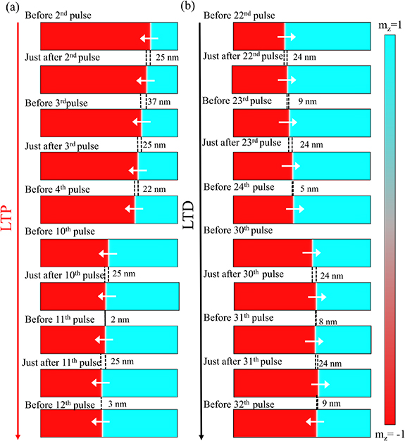
Figure 3. Device without defects: (a) magnetization configuration images 'just after' programming pulse n is applied for LTP and 'before' the next pulse (n + 1) pulse is applied for LTP (the time gap between the two is the delay time between pulses: 100 ns). Here, n = 2, 3, 10, 11. The cyan colour represents vertical up magnetic moments i.e.  , and red represents vertically down state
  . (b) Magnetization configuration images 'just after' programming pulse n is applied for LTD and 'before' the next pulse (n + 1) pulse is applied for LTD (the time gap between the two is the delay time: 100 ns). Here, n = 22, 23, 30, 31. (More details are provided in the text.)
Download figure:
Standard image High-resolution image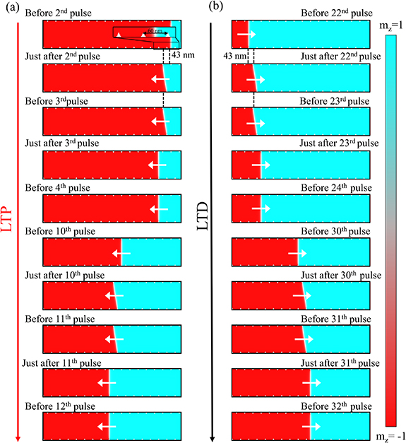
Figure 4. Device with defects: (a) magnetization configuration images 'just after' programming pulse n is applied for LTP and 'before' the next pulse (n + 1) pulse is applied for LTP. Here, n = 2, 3, 10, 11. The cyan colour represents vertical up magnetic moments i.e.  , and red represents vertically down state
  . (b) Magnetization configuration images 'just after' programming pulse n is applied for LTD and 'before' the next pulse (n + 1) pulse is applied for LTD. Here, n = 22, 23, 30, 31. (More details are provided in the text.)
Download figure:
Standard image High-resolution imageAs observed from the magnetization configuration images of figure 3, in the device without defects, the domain wall moves at the velocity of 25 m s−1 during each pulse. Since each pulse is of 1 ns duration, this means the domain wall moves by 25 nm during a pulse, left or right depending upon the current polarity (between 'before' nth pulse and 'just after' n + 1th pulse, n = 2, 3, 10, 11 here). But we also observe from figure 3 that during the delay of 100 ns between one pulse and the next, the domain wall may also move. During LTP, between 'just after 2nd pulse' and 'before 3rd pulse' (the delay between 2nd and 3rd pulse basically), domain wall moves by 37 nm. Similarly in the delay between 3rd and 4th pulse, domain wall moves by 22 nm; between 10th and 11th pulse, it moves by 2 nm; and between 11th and 12th pulse, it moves by 3 nm.
Thus, we observe that for LTP, the domain wall moves much more during the delay times between the initial pulses compared to that between the later pulses. The physical phenomenon responsible for this this is described next. During the initial pulses, the domain wall is located towards the right end of the device; during the delay time between pulses, when spin current is 0, the domain wall still wants to move right towards the centre of the device to minimize the energy due to dipole-dipole interaction (magnetostatic energy). This is further shown in figure 6, which we discuss later. Dipole-dipole interaction energy is minimum when the domain wall is at the middle, with half of the magnetic layer polarized up and half polarized down, as shown both through MOKE imaging experiments and micromagnetic simulations in the report by Bhowmik et al [17]. In our simulation here, during the later pulses, the domain wall is already near the centre of the device; so its tendency to move during the delay time, when charge current and spin current are zero, is much less. This leads to non-linearity of the LTP curve as observed in figure 2(a) (red plot: LTP, black plot: LTD). Using the method associated with the Neuro-Sim simulator [9, 27, 28], we obtain the following: non-linearity coefficient for LTP αP
= 2.47, non-linearity coefficient for LTD  , and thus asymmetry coefficient (
 ) = 4.92 (figure 2(b): red plot for LTP, black plot for LTD). These numbers are comparable to that reported experimentally by Yadav et al [26], which means our micromagnetic modelling here can indeed explain the non-linearity and asymmetry reported experimentally in similar devices [26, 29].
Next, in figure 4, we observe the magnetization configuration images under programming current pulses for the device with edge defects. As mentioned earlier, the pulse width and the delay between two consecutive pulses are kept the same here too as the device without defects: 1 ns pulse width, and 100 ns delay (figure 3). We observe that in this case, during the delay between nth pulse and  th pulse, the domain wall does not move at all, irrespective of whether the domain wall is at the edge of the device or near the centre. The only motion takes place during the pulse. This leads to extremely high linearity and symmetry of the LTP and LTD curves for the device with defects (figures 2(a) and (b): pink plot for LTP, brown plot for LTD).
It is to be noted from figure 2 though that the programming pulses are of higher current density (3 × 10⁷ A cm−2) for the device with defects when compared to that without defects (1 × 10⁷ A cm−2). This is because higher spin current is needed to move the domain wall in the presence of defects. In figure 5, we plot domain-wall velocity vs current density for the device without defects and the device with defects to show this effect. For a given value of current density, domain-wall velocity is obtained by initializing the domain wall at one end of the device in our micromagnetic simulation, applying constant spin current density on the layer of magnetic moments (corresponding to the given current density), measuring and plotting the domain-wall position (from the average out-of-plane magnetization of the magnetic layer) as a function of time, and then calculating the slope of that plot to obtain the domain-wall velocity. From the plot of domain-wall velocity vs current density obtained this way (figure 5), we observe that if the device does not have defects, the domain wall starts moving even at very small current densities. But if the device has defects, the domain wall does not move until the current density crosses a threshold. This finding is consistent with that reported in previous studies on domain-wall motion due to defects [24, 59]. This is why LTP and LTD for the device with defects involves higher current density compared to that for the device without defects (figure 2).
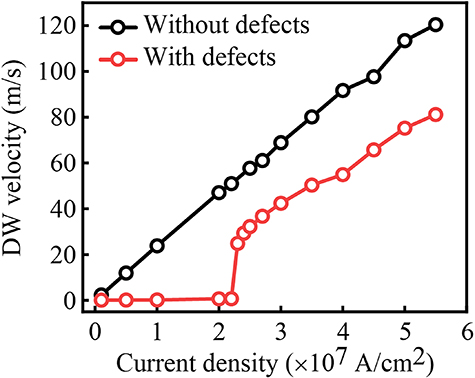
Figure 5. Domain wall (DW) velocity vs current density for the device without defects (black plot) and the one with defects (red plot).
Download figure:
Standard image High-resolution imageFigure 5 also shows that the domain-wall velocity at 3 × 10⁷ A cm−2 current for the device with defects is higher than the domain-wall velocity at 1 × 10⁷ A cm−2 current for the device without defects. As a result, since the pulse width is the same in both cases (1 ns), the domain wall moves farther during every pulse for the device with defects compared to the device without defects. Hence the net change of out-of-plane magnetization over 20 pulses is higher for the device with defects (pink and brown plots) compared to that without defects (red and black plots) in figure 2.
2.3. Role of thermal field
All the above simulations (figures 2–4) have been carried out under zero thermal field. We show next that even in the presence of thermal field (corresponding to different temperature values: 0 K, 50 K, 100 K, 150 K, 200 K, 250 K, 300 K), during the delay time between two programming pulses (100 ns), the domain wall does not move when the defects are present at the edges (figure 6(b)). This leads to very low fluctuation of the average magnetization of the free layer (Mz ) over time (figures 6(b) and (c)). Compared to that, when the defects are absent, the domain wall moves a lot in the absence of programming pulses (100 ns delay) (figure 6(a)) and the corresponding fluctuation in Mz is, hence, about two orders higher than in the case with defects (figure 6(c)). In fact, for the device without defects, after initiating the domain wall at one end of the device like in figure 3, average out-of-plane (OOP) magnetization (mz ) of the ferromagnetic layer increases steadily in the absence of programming pulses, suggesting that the domain wall moves towards the centre to minimize the energy due to dipole interaction between moments. This is the explanation we had earlier provided in this paper to explain the non-linearity of LTP and LTD curves for the device without defects.
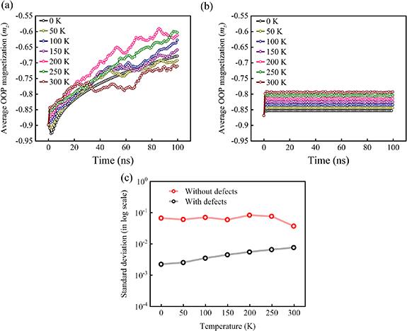
Figure 6. (a) For a device without defects, after initiating the domain wall at one end of the device, like in figure 3, average out-of-plane (OOP) magnetization (mz ) of the ferromagnetic layer increases steadily in the absence of programming pulses, suggesting that the domain wall moves towards the center to minimize the energy due to dipole interaction between moments. This is true at different temperature values. (b) The same simulation as in (a) is carried out for the device with defects. This time mz changes very little in the beginning but then attains a steady value. This is true across a wide range of temperature values (0 K–300 (K). (c) Standard deviation/fluctuation in mz , proportional to the domain-wall motion, is plotted as a function of temperature for the device without defects and the one with defects.
Download figure:
Standard image High-resolution imageThus the phenomenon which leads to improved linearity and symmetry of LTP and LTD (defects prevent the domain wall from moving during the delay time between pulses) is valid even under high thermal fields. Hence, even at finite temperature values (up to room temperature), it is expected that the presence of defects will lead to linear and symmetric LTP and LTD like in figure 2(requirement (iii) for the synapse, as mentioned in section 1). Additionally, if the defects can pin the domain wall and prevent them from moving for 100 ns, it is expected that they will be able to do the same for much longer duration in the absence of programming pulses. Hence, incorporation of defects in the device will make them satisfy the criterion of very long retention time of synaptic states after on-chip learning (requirement (iv) in section 1).
Having shown here that the synaptic states of the device with defects are stable up to room temperature, we would like to point out that various two-dimensional magnetic materials have been recently developed which have Curie temperature higher than room temperature [60–62]. These novel materials can be explored for domain-wall synaptic devices in the near future.
3. On-chip learning in crossbar-array-based LSTM and FCNN
We next discuss how we have incorporated the synaptic characteristics (LTP and LTD) obtained through micromagnetic simulation in section 2 to simulate on-chip learning in crossbar arrays using these devices. Since (to the best of our knowledge) this is the first work showing system-level simulation of a domain-wall-synapse-based LSTM network, we describe our LSTM algorithm (both forward computation and learning) in details in supplementary material accompanying the paper. The LSTM network we have designed is shown at an abstract mathematical level in figure 7 [35, 38]. Details on how forward computation is carried out in the LSTM network and how the network is trained (using back-propagation through time, or BPTT, algorithm [35, 36, 38]) have been mentioned in supplementary material accompanying the paper. Meanings of all the symbols used in figure 7 have also been explained in this section of supplementary material. The FCNN algorithm (both forward computation and learning) that we have used here has been provided in previous reports in details [24, 26].
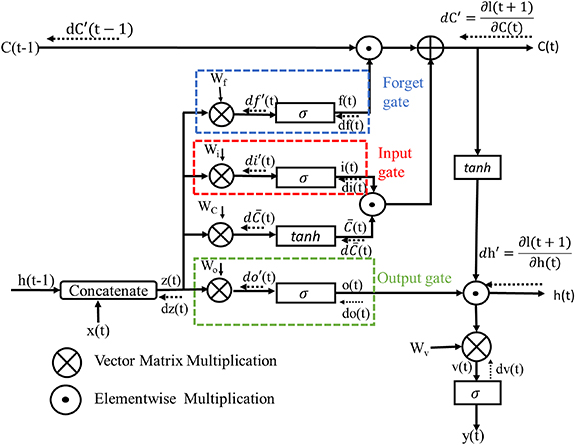
Figure 7. The schematic of the long short term memory (LSTM) network, used here, is shown. The corresponding equations for forward computation and training are provided in supplementary material accompanying the paper. The vector matrix multiplication (VMM) operations in the network, as labelled here, can be implemented through crossbar arrays of domain-wall synapse devices.
Download figure:
Standard image High-resolution imageThe role of the crossbar arrays of non-volatile synaptic devices, like the domain-wall device discussed in this paper, is to implement the vector matrix multiplication (VMM) operations involved in LSTM and FCNN for both forward computation and on-chip learning. To simulate forward computation and on-chip learning in the crossbar-array-based LSTM, equations (1)–(33) of supplementary material have been solved numerically, over iterations, through high-level programming language Python. The weight matrices and biases and their updates do not take ideal values, like in a standard machine learning code, but take realistic values based on how the weights can be stored and updated in domain-wall synapses (as discussed in section 2). The weight update characteristic for each synapse is based on LTP and LTD characteristics obtained through micromagnetic simulation in section 2 for the two kinds of domain-wall synapses (without defects and with defects), with our Python code including all aspects of the LTP and LTD curves obtained in section 2: finite bit resolution, non-linearity, and asymmetry.
The finite bit resolution is incorporated in the following manner in our Python code. Since each synapse device (with or without defects) stores 20 states for LTP and LTD (figure 2), we consider each device to be of 4-bit capacity. To obtain good training performance, we incorporate two such 4-bit devices per synapse cell: one for four least significant bits (LSB) and one for four most significant bits (MSB). The weight updates, as obtained from equations (32) and (33) of supplementary material above, are thresholded to 1 bit only at each iteration, thereby making the peripheral circuitry for on-chip learning simple [24, 63]. When all four LSBs have reached the '1111' state, they are reset to '0000' state and the four MSBs are increased by 1 bit. Similarly, when all four LSBs have reached the '0000' state, they are reset to '1111' state and the four MSBs are decreased by 1 bit.
The domain-wall device with defects exhibits perfectly linear and symmetric LTP and LTD (figure 2: pink and brown plots); so in that case, in our Python code, 1 bit of weight increase/decrease translates to an increase/decrease of the synapse device's conductance by  , where Gmax
is the highest value of conductance of the device and Gmin
is the lowest value of conductance (figure 2). However, the device without defects exhibits non-linearity and asymmetry in its LTP and LTD. So in that case, in our Python code, weight updates vary from
, where Gmax
is the highest value of conductance of the device and Gmin
is the lowest value of conductance (figure 2). However, the device without defects exhibits non-linearity and asymmetry in its LTP and LTD. So in that case, in our Python code, weight updates vary from  by different amounts, based on where on the LTP/LTD curve the weight is currently. Higher the non-linearity (higher value of αP
, αD
), higher is the deviation. We use αP
= 2.47 and
by different amounts, based on where on the LTP/LTD curve the weight is currently. Higher the non-linearity (higher value of αP
, αD
), higher is the deviation. We use αP
= 2.47 and  , in accordance with our micromagnetic simulation results for the device (figure 2: red and black plots).
We carry out our on-chip learning simulation for the LSTM network by training it for a regression task, using the Airline Passengers data set (1949–1960) [35, 37]. The actual data is plotted in black in figure 8. As shown there, sample 1 to sample 96 (data from January 1949 to December 1956) has been used for training, and sample 97 to sample 144 (data from January 1957 to December 1960) have been used for testing.
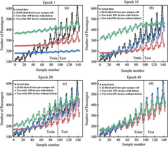
Figure 8. For the Airline Passenger data set, data predicted by the LSTM network with 32-bit ideal synapses (with 32-bit ideal weight update) used in VMM operations have been plotted in blue. Data predicted by the LSTM with 4-bit domain-all devices without defects (highly non-linear and asymmetric of LTP and LTD) have been plotted in green, while that predicted by the LSTM with 4-bit domain-wall devices with defects (highly linear and symmetric LTP and LTD) have been plotted in red. Predictions after 1st epoch (a), 10th epoch (b), 20th epoch (c), and 40th epoch (d) have been shown.
Download figure:
Standard image High-resolution imageData predicted by the LSTM with 32-bit ideal synapses (weight update also has 32-bit precision) have been plotted in green in figure 8. This is basically the same as a standard machine-learning implementation of a LSTM on a conventional computer. This result serves as a benchmark for our on-chip learning simulation results for the LSTM with domain-wall devices without defects and the LSTM with domain-wall devices with defects (simulation carried out as described above), also plotted in figure 8(blue plot: without defects, red plot: with defects). For all the three LSTM networks, the following parameter values are used: size of hidden state = 12, number of time steps (T in equation (32) of supplementary material) = 3, learning rate η = 0.001.  ;
;  ; weights
  ; biases
  ; weights at output layer
  ; bias at output layer
  (figure 7, also refer to supplementary material).
In figure 8, we show the results predicted by the simulated LSTMs after 10th epoch, 20th epoch, 30th epoch, and 40th epoch of the training. For both kinds of devices (with and without defects), after a sufficiently high number of epochs, the predicted data by the LSTM networks using domain-wall synapse devices match with the actual data and that predicted by the conventional-machine-learning-based LSTM model with high bit precision. However, the difference in the performance (for this task) of the LSTM with domain-wall devices without defects and that with domain-wall devices with defects can be understood from the loss vs epoch plot in figure 9. The loss is calculated from equation (9) of supplementary material, for every epoch. It is observed that in the case of the domain-wall synapse with defects (non-linear and asymmetric LTP and LTD), the loss drops very fast in the first few epochs but then attains a steady value much higher than that for the conventional machine-learning-based LSTM model with high bit precision. On the other hand, in the case of the domain-wall synapse with defects (linear and symmetric LTP and LTD), the loss drops after a much higher number of epochs but then slowly reaches a value as low as that for the conventional machine-learning-based LSTM model with high bit precision. Thus the LSTM with domain-wall devices with defects performs better than that with devices without defects, as expected from the much higher linearity and symmetry of LTP and LTD characteristics of the former compared to the latter.

Figure 9. For the Airline Passenger data set, loss vs epoch is plotted during training for the three LSTM networks mentioned in figure 8. With more training time, the performance of the LSTM using domain-wall devices with defects (highly linear and symmetric LTP and LTD) is found to be better than that using domain-wall devices without defects (highly non-linear and asymmetric of LTP and LTD).
Download figure:
Standard image High-resolution imageDegradation of network-level performance because of lack of defects in the domain-wall device and subsequent non-linearity and asymmetry of LTP and LTD is even better reflected when we compare the performance of these devices for a classification task using the MNIST data set (of handwritten classifications). For both devices, we use a FCNN with the input layer containing 784 nodes, only one hidden layer containing 100 nodes, and an output layer containing 10 nodes. The number of train and test samples used are 60 000 and 10 000 respectively. Details on the learning algorithm and the procedure followed to incorporate the LTP and LTD characteristics of the domain-wall devices in the on-chip learning simulation of the FCNN can be found in [24, 26].
As observed in figure 10, the classification accuracy of the FCNN with defect-included domain-wall synapses is higher than that of the FCNN with domain-wall synapses, which do not have defects, by 6%, again because of the much higher linearity and symmetry of the former devices with respect to the latter. This result agrees with the prediction made previously by Sun and Yu [9] and Yadav et al [26] in this context: the prediction that classification accuracy of a crossbar-array-based FCNN degrades with an increase in non-linearity and asymmetry of the LTP and LTD of the corresponding synapses.
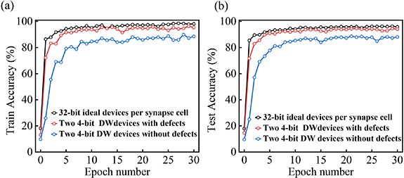
Figure 10. Using the MNIST data set of handwritten digits, classification accuracy numbers for training samples (a) and testing samples (b) are compared for FCNNs with 32-bit ideal synapses (with 32-bit ideal weight updates), domain-wall synapses without defects, and domain-wall synapses with defects. Owing to the much higher non-linearity and asymmetry in LTP and LTD exhibited by the devices without defects, classification accuracy is 6% lower for that case compared to the case of synapse devices with defects.
Download figure:
Standard image High-resolution imageNext, we calculate the energy consumption per weight update pulse (each LTP or LTD step) in the domain-wall device due to Joule heating. We present the energy consumption per pulse, both for the device without defects and the device with defects, in table 1. For this calculation, resistance of the device has been estimated as follows. In the recent experimental report by Yadav et al [26], the resistance of the Co/Pt/SiO2 device (in which LTP and LTD have been experimentally demonstrated) has been measured to be 378 Ω. The Pt layer has been considered to be the dominant contributor to the resistance owing to the much higher thickness of the Pt layer compared to the other layers. In the devices simulated here, since the heavy metal is also considered to be Pt (as mentioned in section 2), we estimate the resistance of our simulated devices from the resistance value measured and reported by Yadav et al [26]. The devices in the report by Yadav et al are 100 µm long and 20 µm wide, while our simulated devices here are 1 µm long and 100 nm wide. So the resistance of each simulated device in our case is estimated to be 756 Ω. For the device without defects, the current density for both LTP-causing and LTD-causing pulses is  A cm−2, while for the device with defects, the current density for both LTP-causing and LTD-causing pulses is
  A cm−2 (figure 2). The duration of each pulse in all cases is 1 ns. So the energy consumption per LTP/LTD pulse for the device without defects is 7.56 fJ, while for the device with defects is 68 fJ.
Table 1. Energy consumed per LTP/LTD pulse for weight update on each domain-wall device and total energy consumed in all the synapse devices over all epochs while carrying out on-chip learning of corresponding LSTM and FCNN crossbar arrays.
| Domain-wall synaptic device | Current density per LTP/LTD pulse | Energy consumed per pulse | Energy consumed across all synapses: LSTM training | Energy consumed across all synapses: FCNN training |
|---|---|---|---|---|
| Without defects |
 A cm−2 A cm−2
| 7.56 fJ | 3.153 nJ | 3.85 µJ |
| With defects |
 A cm−2 A cm−2
| 68 fJ | 13.25 nJ | 44 µJ |
Based on these energy-consumption-per-pulse values and the the total number of weight updates across all synapses over all epochs, we have estimated in table 1 the total energy consumed in the domain-wall synapse devices of the crossbar arrays during training of the LSTM and FCNN networks in this work. It is to be noted that the energy consumption in the peripheral circuits accompanying the crossbar arrays have not been considered here. This is because the peripheral circuit's energy consumption is mostly independent of whether the synaptic device has defects or not. Since this work is about comparing the performance of a network of devices with defects with that of devices without defects, the peripheral circuit's energy consumption is not very relevant here.
4. Discussions
4.1. Device fabrication feasibility
The edge defects we have simulated here are material defects, or regions with a modified PMA value compared to the rest of the ferromagnetic layer. Experimentally, this can be achieved through focussed ion beam irradiation, as shown recently by Dunne et al [64]. On the contrary, as mentioned in section 1, the defects in the device reported by Liu et al [33] are geometrical defects (like notches or grooves), and to the best of our understanding, they need a high-precision etching tool (as opposed to a focused ion-beam irradiation tool) for fabrication. Hence, future fabrication feasibility of the device with geometric defects reported by Liu et al [33], as well as for our device with material defects (modified PMA), depends upon the availability of specific fabrication tools to the researchers pursuing the work.
4.2. Novel materials
In previous experiment-based and simulation-based reports on spin-orbit-torque-driven domain-wall motion in heavy metal/ferromagnetic metal hetero-structures, it has been shown that an antisymmetric exchange interaction at the interface, Dzyaloshniskii–Moriya Interaction (DMI), enhances the spin orbit torque and hence the domain-wall velocity [14–16, 19]. Subsequently, in a recent report by Sahu et al [65], it has been shown both through micromagnetic and system-level simulations that higher domain-wall velocity leads to lower magnitude current pulses or shorter duration current pulses (or both) for LTP/LTD of domain-wall synapse devices. This reduces the net time and energy for on-chip learning in crossbar arrays of such devices by orders of magnitude. Recently, it has been shown that interfacial DMI gets significantly enhanced when the magnetic layer is extremely thin (one monolayer or so) [66]. So exploring these novel materials for synaptic device applications, owing to their high interfacial DMI, will be interesting.
4.3. Scaling issues
As stated in section 2, the length of our simulated device (the ferromagnetic layer in which the domain wall moves) is 1000 nm and the width is 100 nm. Our device dimensions are about one order lower than that of the domain-wall devices experimentally demonstrated thus far [26, 29, 31, 32]. Also, they are of comparable size as the domain-wall devices reported through simulation [31], if they have to store synaptic weights of the same bit resolution.
Next, we discuss how much further can we shrink the dimensions of our domain-wall synapse device without decreasing bit resolution of the synaptic weight stored in it. (Reduction in bit resolution leads to significant reduction in on-chip learning accuracy of the corresponding crossbar arrays [6, 9].) Currently, the gap between two consecutive defects on either edge of our device is 60 nm (as stated in section 2), and this gap cannot be reduced below the domain-wall width. In our micromagnetic simulation, PMA constant (K) =  J m−3, and exchange-correlation constant (A) =
  J m−1. So the domain-wall width can be estimated by the expression
  [67] and is equal to 12 nm approximately for our device, which is in the same order of magnitude as that reported experimentally for similar PMA-exhibiting heavy metal/ferromagnet hetero-structures [68, 69].
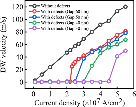
For scaling without losing bit resolution, we can simply try to reduce the distance between consecutive defects from its current value (60 nm) close to the domain-wall width (≈12 nm in our case). The length of the device will be roughly equal to the product of number of conductance/weight levels (exponential of bit resolution) and distance between two consecutive defects. In figure 11, we plot domain-wall velocity vs current density for different distances between notches: 60 nm, 50 nm, 40 nm, and 30 nm (the corresponding device lengths for a 4-bit device are listed in table 2). The method for domain-wall velocity calculation is same as for figure 5. We observe from the above figure that even if the defects on either edge come closer (from 60 nm to 30 nm), it is still possible to move the domain wall almost at the same velocity as before; it is just that the current density for doing so increases. However, if the distance between two gaps decreases, the distance that the domain wall needs to cover during one LTP/LTD pulse goes down, leading to decrease in the pulse duration (as shown in table 2). Thus, as the device length is scaled down, the programming current density and current increases, pulse duration decreases, and the resistance of the device decreases (since length of the device decreases).
Figure 11. Domain wall (DW) velocity vs current density for different gap lengths between consecutive defects.
Download figure:
Standard image High-resolution image
Table 2. Table showing how duration of LTP/LTD pulse and energy dissipated per LTP/LTD pulse scale with length of the device (which is in turn proportional to the distance between two consecutive defects), while the synaptic weight resolution of the device has been kept fixed at 4 bits.
| Distance between defects | Length of 4-bit device | Current density for LTP/LTD | Duration of LTP/LTD pulse | Energy dissipated per pulse |
|---|---|---|---|---|
| 60 nm | 960 nm |
 A cm−2 A cm−2
| 1.41 ns | 91.87 fJ |
| 50 nm | 800 nm |
 A cm−2 A cm−2
| 1.35 ns | 73.38 fJ |
| 40 nm | 640 nm |
 A cm−2 A cm−2
| 0.86 ns | 66.32 fJ |
| 30 nm | 480 nm |
 A cm−2 A cm−2
| 0.75 ns | 67.87 fJ |
In table 2, we also estimate the energy dissipated due to Joule heating per LTP/LTD pulse. We observe that the energy dissipated per pulse, which is the product of resistance, pulse duration, and the square of current, decreases slightly as the distance between defects, and hence device length, is scaled down. Thus, our domain-wall device can be scaled down to ≈500 nm without increase in pulse duration (hence without reduction of speed for on-chip learning) or increase in energy dissipation per pulse (hence without increase in overall energy dissipation for on-chip learning on the crossbar array of these devices). Hence, our proposed technology is scalable down to 500 nm device length, without the need for novel innovations in terms of materials.
But to scale even below 500 nm without losing bit resolution, material-level innovations are needed. Novel ferromagnetic, anti-ferromagnetic, and ferrimagnetic materials can be explored in which the domain wall is of much smaller size than the presently explored material. Alternatively, instead of domain walls, skyrmions can be used to store synaptic states. Magnetic skyrmions have been shown to be of much smaller size compared to magnetic domain walls. Recently, skyrmionic synaptic devices with about 20 synaptic states (4-bit precision) have been experimentally demonstrated [70]. With this kind of materials-related innovations, the device dimensions can be reduced further down without sacrificing synaptic bit resolution, and hence without sacrificing accuracy of on-chip learning in the corresponding crossbar arrays.
5. Conclusion
Thus, in this paper, we have first shown through micromagnetic simulations that material defects (regions with modified PMA compared to the rest of the ferromagnetic layer) at the edges of a domain-wall synapse device act as pinning centres for the domain wall and prevent the domain wall from drifting when programming current pulses are not applied. We show that this improves the linearity and symmetry of the LTP and LTD characteristics of the devices significantly. Next, we simulate on-chip learning in LSTM networks and FCNNs, based on crossbar arrays of these domain-wall synapse devices, and show that the improvement in linearity and symmetry of LTP and LTD leads to significant improvement in on-chip learning performance of the LSTM and FCNNN. We also estimate the energy consumption in these synaptic devices and project their scaling, for on-chip learning in corresponding crossbar arrays.
Data availability statement
All data that support the findings of this study are included within the article. The data used to train the LSTM network in this paper (Airline Passenger data set: 1949–1960) can be accessed freely at: www.kaggle.com/datasets/rakannimer/air-passengers. The data used to train the FCNN network (MNIST data set of handwritten digits) can be accessed freely at: http://yann.lecun.com/exdb/mnist/.
All data that support the findings of this study are included within the article (and any supplementary files).
Supplementary data (5.0 MB PDF)