
Abstract
Ferroelectric memory devices with fast-switching speed and ultra-low power consumption have been recognized as promising building blocks for brain-like neuromorphic computing. In particular, ferroelectric memories based on 2D materials are attracting increasing research interest in recent years due to their unique properties that are unattainable in conventional materials. Specifically, the atomically thin 2D materials with tunable electronic properties coupled with the high compatibility with existing complementary metal-oxide-semiconductor technology manifests their potential for extending state-of-the-art ferroelectric memory technology into atomic-thin scale. Besides, the discovery of 2D materials with ferroelectricity shows the potential to realize functional devices with novel structures. This review will highlight the recent progress in ferroelectric memory devices based on 2D materials for neuromorphic computing. The merits of such devices and the range of 2D ferroelectrics being explored to date are reviewed and discussed, which include two- and three-terminal ferroelectric synaptic devices based on 2D materials platform. Finally, current developments and remaining challenges in achieving high-performance 2D ferroelectric synapses are discussed.
Export citation and abstract BibTeX RIS

Original content from this work may be used under the terms of the Creative Commons Attribution 4.0 licence. Any further distribution of this work must maintain attribution to the author(s) and the title of the work, journal citation and DOI.
1. Introduction
With the emergence of artificial intelligence, machining learning, and internet-of-things, a vast increase in the number of data workloads has triggered new challenges in improving computation speed and energy efficiency. However, the conventional computing systems based on von Neumann architecture are encountering limitations in meeting the data-abundant processing requirements due to the instructions transfer latency between memory and central processor, commonly known as the memory wall [1–4]. One revolutionary approach makes use of a radically different neuromorphic computing architecture to solve the bottleneck of von Neumann-based-computing [5, 6]. Such a novel computing system is inspired by the neuro-synaptic frameworks in the human brain that possess superior functionalities of parallel computing and adaptive learning with an ultra-low total power consumption of 20 W and an operation power consumption of 1–100 fJ per stimulus, respectively [7]. By means of neuromorphic computing, many computation calculations can be processed at the same location where the data is located, resulting in improved processing speed. In essence, artificial synapses are used in neuromorphic computing to emulate the biological synapses, which can update and memorize internal conductivity known as synaptic weight in response to external stimulations.
To date, extensive investigations have been made to emulate the synaptic functionalities via electronic and optoelectronic devices for neuromorphic computing. Specifically, the emerging artificial synapses are primarily realized by post-CMOS devices, such as phase-change memory (PCM) [8], resistive random-access memory (RRAM) [9, 10], magnetoresistive random-access memory (MRAM) [11], ferroelectric random-access memory (FeRAM), ferroelectric field-effect transistor (FeFET) [12, 13], etc. Among these, the ferroelectric-based memory devices possess the advantages of ultra-fast write/read speed and ultra-low power consumption, offering great potential for the practical implementation of high-performance synaptic devices for neuromorphic computing. Ferroelectric materials have been persistently studied since the discovery in oxide perovskites with the key feature of the sustainability of multiple stable polarization states, which can switch between each other by applying an external electric field. Substantial efforts have been devoted to scaling the thickness of ferroelectric films (such as PbTiO3, BaTiO3 (BTO), BiFeO3 (BFO), and doped HfO2) for achieving higher density and lower power consumption [14–17]. For example, it has been reported that ferroelectricity can be obtained in a 1 nm Zr-doped HfO2 [17]. However, the performance of ferroelectric polarization will inevitably degrade when the conventional ferroelectric materials approach the fundamental thickness limit, resulting from the surface-related effects and enhanced depolarization field. Besides, the synthesis of high-quality and ultra-thin traditional ferroelectric films requires an elaborate design of lattice-matched growth substrates and a complicated fabrication process, limiting their practical implementation of low-dimensional ferroelectric memory devices for neuromorphic computing.
In recent years, two-dimensional (2D) materials have attracted tremendous research interest due to their unique intrinsic properties, such as the atomic structures, complementary metal-oxide-semiconductor (CMOS) compatibility, and superior electronic and optoelectronic properties [18–22]. Leveraging on these merits, high-performance artificial synapses based on 2D materials have been intensively developed [23–28]. In particular, they have been widely employed as active materials in diode-type artificial synapses via various mechanisms, such as the formation of filaments, the transformation of phases, vacancy migration, charge trapping, etc [29–31]. Additionally, they can also be integrated into transistor-type devices with heterostructures to realize synaptic behaviors. More recently, a considerable number of 2D materials (such as WTe2, d1T-MoTe2, SnTe, CuInP2S6 (CIPS), BA2PbCl4, α-In2Se3, β'-In2Se3, 2H α-In2Se3, SnSe, and SnS) are found to possess ferroelectricity property [32–41]. Besides, other non-ferroelectric 2D materials can also be easily converted into stable ferroelectric polarization materials by various external factors such as doping, strain engineering, surface modification, and defect engineering [42–45]. Compared to conventional ferroelectric materials, they allow easier integration into substrates owing to their strong intralayer coupling and weak interlayer interaction. Therefore, ferroelectric 2D materials show great potential to realize low-dimensional functional devices for neuromorphic computing with novel structures. Apart from that, some non-ferroelectric 2D materials are projected to be superior channel materials and have been exploited for realizing high-performance transistors owing to their high mobility and compatibility with other CMOS technology boosters. In particular, they could potentially overcome the limitation of charge traps-induced degradation in conventional ferroelectric-Si-based FeFETs. For example, a few works have demonstrated that they are promising candidates to be used in FeFETs integration for synaptic applications by combining with conventional ferroelectric gate stack (such as Zr-doped HfO2, poly(vinylidene fluoride/trifluoroethylene) [P(VDF-TrFE)], and PbZrx Ti1−x O3). Therefore, a comprehensive review on this topic is timely and sought after [46–48].
In this review, we first briefly compare the different memory technologies and discuss the merits of employing ferroelectric-based memory technology for neuromorphic computing. In the following section, a range of experimentally discovered 2D ferroelectric materials are introduced. Various functional ferroelectric memory devices based on 2D materials for neuromorphic computing applications are then reviewed. Finally, the existing challenges and outlook in this rapidly progressing research field are discussed.
2. Memory technologies for neuromorphic computing
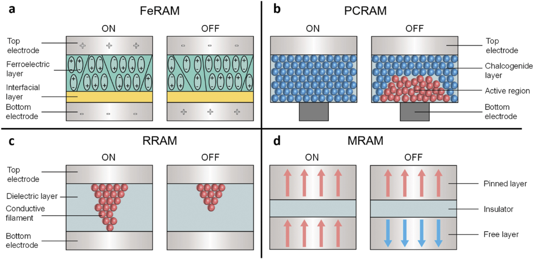
Various memory technologies have been exploited to realize hardware artificial neural networks (ANNs), such as FeRAM, PCRAM, RRAM, and MRAM. Figure 1 shows the different working mechanisms of these representative memory technologies. For example, FeRAM consists of a metal–ferroelectric-metal (MFM) stack and relies on the polarization switching of the ferroelectric materials, as shown in figure 1(a). By applying an external voltage to the MFM stack, the ferroelectric dipoles inside the ferroelectric layer change their orientation, known as ferroelectric switching. This switching mechanism is also exploited to result in resistance modulation in FeFETs [49, 50]. By changing the dielectric polarization, the resistance of the channel material in FeFET can be modulated, which enables the realization of the synaptic transistor. In contrast, PCRAM, RRAM, and MRAM are resistive switching memories, in which their physical switching results in a direct resistance change, as illustrated in Figures 1(b)–(d). For example, in PCRAM, the resistance switching effect is caused by the phase conversion between the amorphous and crystalline states of the chalcogenide layer with the effect of Joule heating under the application of voltage pulse [51, 52]. RRAM with a metal–insulator–metal structure achieves two different resistance states resulting from the filament formation either by oxygen vacancy or metal atoms motion when a soft breakdown voltage is applied [53, 54]. In contrast, MRAM exploits the characteristic of electron spin to achieve data storage [11, 55]. The resistance change across the barrier is caused by the different configurations of the magnetic moments in the two electrodes. Because of the different working principles for the memory technologies, each option has its appealing characteristics compared with others, which determines its use in specific applications.

Figure 1. Different mechanisms of the representative emerging memory technologies including FeRAM, PCRAM, RRAM, and MRAM. (a) Structure of the FeRAM device, where a ferroelectric layer is sandwiched between two metal electrodes. The ferroelectric polarization is generated by applying an external voltage. (b) Structure of the PCRAM device, where a chalcogenide active layer is sandwiched between two metal electrodes. The crystallization process in the active layer gradually converts the device from HRS to LRS when the applied voltage is below the melting voltage, while the amorphization process switches the device from LRS to HRS when the applied voltage is above melting voltage. (c) Structure of the RRAM device, where a dielectric layer is sandwiched between two metal electrodes. The change in resistance states originates from the formation and deformation of conductive filaments. (d) Structure of the MRAM device, where an insulator layer is sandwiched between two ferromagnetic metal electrodes. The resistance change across the barrier is caused by the different configurations of the magnetic moments in the two electrodes.
Download figure:
Standard image High-resolution imageTable 1 compares the performance among the emerging memory technologies and the typical memory technologies [56]. Overall, ferroelectric-based memory technologies (FeRAM, FeFET, and FTJ) exhibit fast write/read speed, long retention, high endurance, and low write energy consumption. These superior properties manifest their great potential for achieving high-performance synaptic devices in neuromorphic computing. However, using conventional ferroelectric materials as the active layer for ferroelectric-based memory devices is faced with scaling issues [57, 58]. This is because the thickness of the ferroelectric materials typically ranges from a few tens-to hundreds of nanometers, which are known as bulk ferroelectrics. Although the discovery of doped HfO2 shows ferroelectricity in the ultra-thin film that may enable device scaling, however, the ferroelectric polarization is dramatically suppressed [17]. This is because some size-dependent factors are becoming dominant, which are previously negligible in their bulk counterparts. For example, the enhanced depolarization field and surface-related effects in the low-dimension film could inevitably degrade the performance of ferroelectric polarization. Besides, the growth of thin-film requires either an elaborate design of lattice-matched growth substrates or a complicated fabrication process. The constraints of conventional ferroelectrics limit further development of low-dimensional ferroelectric-based memory devices for neuromorphic computing. Therefore, focused efforts are needed to explore other potential ferroelectric materials, which have atomic-scale thickness and can be switched using ultra-low voltage. Additionally, FeFET realized by the direct integration of conventional ferroelectric gate stack with silicon suffers from reliability issues. The charge traps at the ferroelectric-Si interface result in parasitic effect, eventually leading to charge injection and information loss. To overcome this issue, non-ferroelectric 2D channel materials are being investigated to replace the traditional channel materials due to its dangling-bond free surface.
Table 1. Benchmark of the memory technologies.
| Technology | SRAM | DRAM | NAND | RRAM | PCM | MTJ | FeRAM | FeFET | FTJ |
|---|---|---|---|---|---|---|---|---|---|
| Cell elements | 6T | 1T1C | 1T | 1T1R | 1T1R | 1T1C | 1T1C | 1T | 1R |
| Cell area | >100 F2 | 6 F2 | <4 F2 | 4–12 F2 | 4–30 F2 | 6–50 F2 | 22 F2 | 6 F2 | 4 F2 |
| Write voltage | <1 V | <1 V | >10 V | <3 V | <3 V | <1.5 V | <3 V | <5 V | <4 V |
| W/R time | 0.3 ns | <10 ns | 0.1 ms | 10 nm | 50 ns | 20 ns | <5 ns | <4 ns | <1 ns |
| Retention | 0 | 64 ms | >10 years | >10 years | >10 years | >10 years | >10 years | >10 years | >10 years |
| Endurance | >1016 | >1016 | >105 | 106–1012 | 106–109 | >1015 | >1014 | >1010 | >107 |
| Write energy | ∼0.7 fJ | ∼5 fJ | ∼10 fJ | ∼0.1 pJ | ∼10 pJ | ∼0.1 pJ | ∼30 fJ | <10 fJ | <5 fJ |
| Suitability for DNN training | No | No | No | No | No | No | No | Moderate | Moderate |
| Suitability for SNN applications | Yes | Yes | No | Yes | Yes | Moderate | Yes | Yes | Yes |
3. 2D ferroelectrics for neuromorphic computing
Recently, substantial attention has been devoted to exploring 2D ferroelectrics, and many 2D materials have been theoretically examined to possess ferroelectricity [32–41, 59–62]. With improved fabrication and advanced characterization techniques, the ferroelectricity could be observed in ultrathin films down to several unit cells. To date, around ten 2D ferroelectric materials have been experimentally examined including WTe2, d1T-MoTe2, SnTe, CuInP2S6(CIPS), BA2PbCl4, α-In2Se3, β'-In2Se3, 2H α-In2Se3, SnSe, and SnS.
Tellurium-based 2D ferroelectric materials have attracted tremendous attention recently since they can be either semiconductors or semimetals. For example, Fei et al reported that semimetal WTe2 with thickness down to two- or three-layer would exhibit spontaneous out-of-plane electric polarization when subjected to gate bias [32]. The switching behavior would exist at room temperature, but vanishes when the temperature rises above 350 K. Yuan et al further observed out-of-plane ferroelectricity in monolayer d1T-MoTe2 at room temperature by using the piezoresponse force microscopy (PFM) [33]. They claimed that the ferroelectricity in d1T-MoTe2 was originating from the spontaneous symmetry breaking owing to the atomic displacements of Mo and Te atoms. Furthermore, K. Chang experimentally demonstrated that stable in-plane spontaneous polarization could be obtained in atomic-thick SnTe down to a 1-unit cell limit [34].
Furthermore, the first ferroelectric CIPS with thickness down to ∼50 nm was experimentally investigated by Belianinov et al [60], as evidenced by domain structures, rewritable polarization, and hysteresis loops, showing the potentials to obtain ferroelectric CIPS down to nanoscale regime. With new advances, room temperature ferroelectricity in CIPS as thin as 4 nm with a transition temperature of ∼320 K was reported by Liu et al [35]. The ferroelectric polarization was generated due to the displacement of the copper sublattice from the centrosymmetric positions to the indium sublattice. The stable polarization could be obtained in ultra-thin thickness owing to the reduced depolarization field inside CIPS with the anti-alignment dipoles.
Moreover, experimental observation of out-of-plane polarization in multilayer α-In2Se3 was reported by Zhou et al [36]. The distinct ferroelectric domains were observed by PFM. In the meantime, the correlation between in-plane and out-of-plane polarization is detected, originating from the lateral movement of the central Se atomic layer induced by an external electric field. C Zheng et al have also reported room-temperature in-plane ferroelectricity in β'-In2Se3 [38]. They further showed that stable ferroelectricity could be achieved in both bulk and thin-layer In2Se3. More recently, another two Tin-based 2D materials, including SnSe and SnS have been experimentally examined to be ferroelectrics by Wang et al and Kwon et al, respectively [40, 41]. By using PFM, the SnSe shows out-of-plane polarization behavior, while SnS shows the in-plane polarization behavior with a relatively large remnant polarization (Pr) of 2Pr ∼ 40 μC cm−2. Table 2 summarizes the experimentally examined ferroelectric 2D materials. All these experimental discoveries of 2D ferroelectrics indicate their potential for achieving next-generation ferroelectric memory devices for neuromorphic computing.
Table 2. Summary of the experimentally examined ferroelectric 2D materials.
| Material | Polarization | Thickness | Characterization | Pr | Ec | Tc(K) | Reference |
|---|---|---|---|---|---|---|---|
| obtaining ferroelectricity | method | ||||||
| SnS | In-plane | 3.7–8.1 nm | P–E measurement | ∼17.5 μC cm−2 | ∼20 kV cm−1 | 873 | 41 |
| WTe2 | Out-of-plane | 1.4 nm | I–V measurement | — | — | 350 | 32 |
| d1T-MoTe2 | Out-of-plane | 0.8 nm | PFM | — | — | RT | 33 |
| SnTe | In-plane | 0.63 nm | STM | — | — | 270 | 34 |
| CuInP2S6 | Out-of-plane | 4 nm | PFM | — | — | 315 | 35 |
| BA2PbCl4 | In-plane | 4 nm | PFM | — | — | 453 | 36 |
| α-In2Se3 | In-plane/Out-of-plane | 10 nm | PFM | — | — | RT | 37 |
| β'-In2Se3 | In-plane | 100 nm | PFM | — | — | 473 | 38 |
| 2H α-In2Se3 | In-plane/Out-of-plane | 1.2 nm | PFM | — | — | RT | 39 |
| SnSe | Out-of-plane | 28 nm | PFM | — | — | — | 40 |
4. Ferroelectric memory devices based on 2D materials for neuromorphic computing
With the rapid progress in ferroelectric materials, non-volatile ferroelectric memory devices based on 2D materials have been widely investigated for neuromorphic computing applications. Generally, the non-volatile ferroelectric memory are classified into FeRAM, FTJ, and FeFET, and the device structures are defined according to the integration process. Specifically, two common structures are implemented, namely two-terminal and three-terminal devices. A two-terminal device is generally used for FeRAM applications. It is primarily a ferroelectric memristor with a MFM sandwich structure, which is easy to be integrated and has high endurance. However, the use of this structure for complex tasks is impeded by disadvantages, such as abrupt switching of the memristor, sneak current paths, and disturbance from adjacent cells. Thus, it is typically combined with a transistor to form a one-transistor-one-resistor (1T1R) or one-transistor-one-capacitor (1T1C) memory cell to construct the ANNs. These selector transistors are laid out next to the memory cell and therefore take up more space. A three-terminal device is primarily used for the FeFET application, where the ferroelectrics serve as the gate dielectric in a three-terminal transistor structure. These devices exhibit different switching mechanisms based on the active switching material and device configuration. A FeFET cell can be its selector, eliminating the additional device and allowing for a more compact memory array. However, conventional ferroelectric-Si FeFETs meet challenges in enhancing the retention time and suppressing parasitic effects such as charge traps at the interface. By replacing the Si channel with 2D semiconductors, it could potentially tackle defective surface-induced performance degradation on account of 2D semiconductors' dangling bond-free pristine surface and counter short-channel effect for ultra-scaled devices owing to the ideal electrostatics.
In the following section, we will review the latest reported two- and three-terminal ferroelectric memory devices based on 2D materials and their switching mechanisms for neuromorphic computing.
4.1. Two-terminal devices
2D ferroelectric materials-based two-terminal devices are usually referring to devices with ferroelectric materials sandwiched between the top and bottom electrodes. Here, we describe the resistive switching mechanism of a two-terminal device with Pt/ferroelectric/NSTO sandwich structure, as shown in figure 2. Assuming that there is no contribution from the ferroelectric polarization in the as-grown films, and a depletion region will be formed in the ferroelectric/NSTO p–n junction after dynamic equilibrium, which would bend the energy band and induce a potential barrier at the interface [63–65]. When a positive voltage pulse is applied on the top metal electrode, the polarization in ferroelectric will be downward and the positive polarization bound charges will accumulate at the ferroelectric/NSTO interface. As a result, the negative electron carriers in NSTO are attracted by the positive bound charges and moved towards the ferroelectric/NSTO interface, causing a decrease in depletion width, as shown in figure 2(a). On the contrary, the polarization in ferroelectric will be upward with a negative voltage pulse. The negative polarization bound charges will aggregate at the interface after a negative voltage pulse is applied on the top electrode. As a result, the electrons carriers in NSTO are repelled by the negative bound charges at the interface, thus increasing the depletion width as shown in figure 2(b). The depolarization field with opposite direction to the polarization is formed in the ferroelectric layer owing to the incomplete screening of the bound charges [66]. Consequently, the energy band will bend at the interface, as shown in figures 2(c) and (d). The potential barrier is lower with a positive voltage pulse compared with that of a negative voltage pulse [67]. Hence, the carriers can pass through the depletion region in the presence of an electric field induced by a positive pulse due to a relatively narrow depletion width and a low barrier height. As a result, the device is switched to a low resistance state (LRS). Then, the depletion width and barrier height will gradually increase owing to the increasing opposite polarization after consecutive negative pulses are applied, resulting in a continuous increase of resistance. Contrarily, the device will be set to a high resistance state (HRS) initially with upward polarization when subjected to external negative pulses. Then, followed by positive voltage pulses, the resistance will continuously decrease with increasing positive pulse amplitude. Thus, the memristive behavior in the sandwich structure could be attributed to the modulation of ferroelectric polarization in terms of the depletion width and potential barrier height. In the following, various 2D ferroelectric-based two-terminal devices are discussed.

Figure 2. Working mechanism of two-terminal ferroelectric-based memory devices. (a) and (b) Schematic showing the charge distribution in the Pt/ferroelectric/NSTO structure under LRS and HRS, respectively. (c) and (d) Energy-band diagrams of the Pt/ferroelectric/NSTO structure at LRS and HRS. Reprinted from [65], with the permission of AIP publishing.
Download figure:
Standard image High-resolution image4.1.1. CIPS-based two-terminal devices
The CIPS consists of a sulfur framework with the octahedral voids filled by Cu, In, and P–P triangular patterns. Bulk crystals are composed of vertically stacked, weakly interacting layers packed by van der Waals interactions, as shown in figure 3(a). The ferroelectricity of CIPS was comprehensively studied by Liu et al [35]. They demonstrated that the ferroelectricity could even be obtained in ultra-thin CIPS with a thickness of 4 nm as characterized by PFM in figure 3(b). Following this discovery, Wu et al reported a CIPS/graphene 2D vdW heterostructure-based FTJ [68]. The tunneling electroresistance (TER) results from the reversed polarization of the ferroelectric CIPS layer, causing a change in the electrical conductance of FTJ. The as-fabricated FTJ exhibited a giant TER of over 106, which can reach 107 by scaling down the thickness of graphene to a monolayer. Besides, data retention characteristics of the device were measured, showing an extrapolated retention of over ten years with a TER above 107. Moreover, the TER remains above 106 after 5000 cycles and could potentially retain after one million switching cycles by extrapolation. This work shows the potential of using CIPS as the ferroelectric layer to realize high-performance FTJ applications.

Figure 3. CIPS-based two-terminal devices. (a) The crystal structure of CIPS, and direction of the out-of-plane polarization is indicated by the arrow. (b) The PFM phase images for 400 nm, 30 nm, 4 nm CIPS flakes and the corresponding PFM amplitude/phase hysteresis loops, respectively. (c) and (d) Optical image and the schematic structure of the Ti/CIPS/Au arrays. (e) and (f) The synaptic behaviors of SADP and SRDP in a Ti/CIPS/Au ferroelectric diode, respectively. (g) and (h) The corresponding PPF and STDP characteristics, respectively. (i) Conductance maps of the 3 × 3 crossbar array after programmed into three patterns. (a) and (b) Reproduced from [35]. CC BY 4.0. (c)–(i) [69] John Wiley & Sons. © 2020 Wiley‐VCH GmbH.
Download figure:
Standard image High-resolution imageBeyond the demonstration of CIPS-based FTJ, Li et al reported a vertical Au/CIPS/Ti diode-based electronic synapse as shown in figures 3(c) and (d), in which the synaptic weight is represented by the conductivity of the diode [69]. The device exhibited resistive switching with a ratio of larger than 6 × 10³ resulting from the ferroelectric switching. The device also exhibited synaptic behavior such as potentiation, depression, and spike-amplitude-dependent plasticity (SADP) with a minimum power consumption per spike of 5.63 pJ by applying external pulse trains, as shown in figure 3(e). Simultaneously, the device showed significant spike-rate-dependent plasticity (SRDP) by modulating the interval time between two applied pulses, as depicted in figure 3(f). Additionally, the synaptic features of paired-pulse-facilitation (PPF) and paired-pulse-depression (PPD) were well emulated, as shown in figures 3(g) and (h). The weight change under both PPF and PPD was larger when the interval time between two pulses was decreased. A time constant of 12.2 ms and 10.8 ms for PPF and PPD were extracted by exponential fitting, respectively, which are comparable to typical biological synapses. A 3 × 3 crossbar array was fabricated to demonstrate the capability for pattern memory applications. By programming the corresponding cell into either potentiation or depression state, the pattern learning process can be realized and the memorized letters could then be retrieved with a read voltage as shown in figure 3(i).
4.1.2. Sn-based two-terminal devices
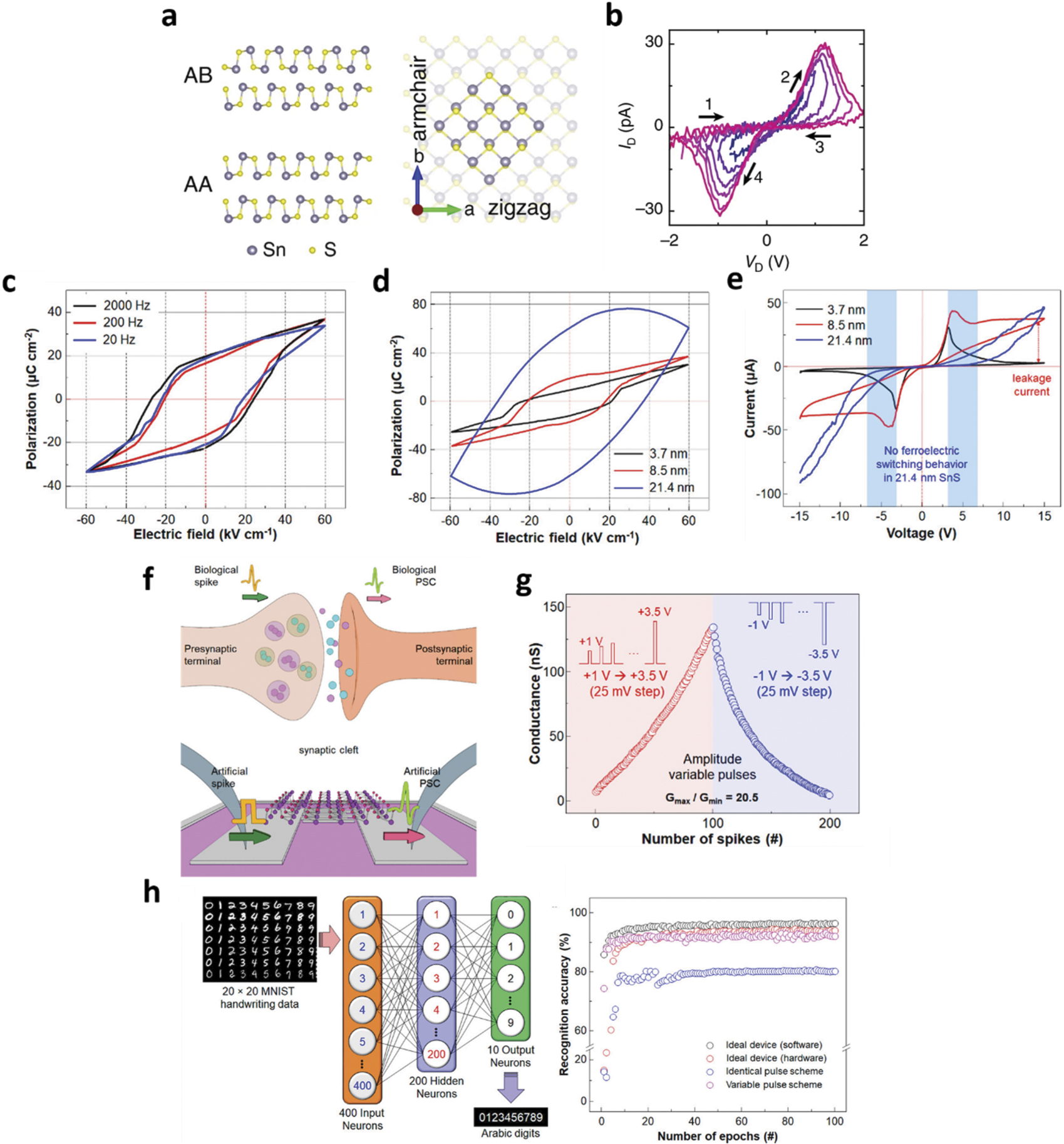
The ferroelectricity of Sn-based 2D materials, including SnS and SnSe, has been experimentally examined. As shown in figure 4(a), the in-plane ferroelectricity of SnS shows the odd–even effect arising from the stacking sequence of the centrosymmetric AB stacking [62]. The ferroelectric switching behavior was observed in the two-terminal lateral structure as shown by the ID–VD measurement in figure 4(b). Kwon et al evaluated the ferroelectricity of CVD-grown polycrystalline SnS by directly performing the polarization-electric field (P–E) measurements using ferroelectric tester [41]. The SnS film exhibited ferroelectric behavior with a remnant polarization of ∼17.5 μC cm−2 and a coercive field of ∼±20 kV cm−1 under different sweep frequencies ranging from 20 Hz to 2 kHz, as shown in figure 4(c). They further revealed that Sn film exhibited a thickness-dependent ferroelectric response and that a Sn film with less than 6 nm thickness shows the strongest ferroelectric response. As shown in figure 4(d), the P–E curves' shape gradually changes to a round circle as the film thickness increases, indicating that the ferroelectricity is diminishing and becomes a resistor-like semiconductor. (See figure 4(d).) Such a round-shaped P–E hysteresis loop was attributed to the leakage caused by charge screening since the thicker film has a smaller gap and lower resistivity, in agreement with the I–V measurement results, as shown in figure 4(e). Whereas, the hysteresis with low leakage current is observed for ultrathin SnS films with a thickness of <6 nm due to its lower carrier density and larger bandgap. The SnS-based two-terminal artificial synapse was then integrated and schematically illustrated in figure 4(f). The device achieved a high Gmax/Gmin ratio, symmetric, and ideal linearity in synaptic weight updates by applying an incremental voltage spike scheme as shown in figure 4(g). Using the Modified National Institute of Standard and Technology (MNIST) database of handwritten digits [70, 71], supervised learning was carried out with ANN simulation, as shown in figure 4(h). During the training, the SnS-based artificial synapses were trained by two different voltage pulse schemes: identical pulse scheme and variable pulse scheme. For identical pulse scheme, the authors used a fixed pulse amplitude during potentiation and another constant amplitude during depression (+3V/−3V, +4V/−4V, and +5V/−5 V). This scheme leads to high nonlinearity of the conductance and low recognition accuracy. On the contrary, the variable pulse scheme utilizes nonidentical pulse amplitude during the potentiation and depression of the synapse. The detailed pulse waveform of the variable pulse scheme is shown in figure 4(g), showing an improved linearity. This scheme achieved 92.1% accuracy after 100 pulse trains and are comparable to the 93.9% recognition accuracy of the ideal hardware-based synaptic devices. Besides, a ferroelectric SnSe-based two-terminal device was proposed to be a promising candidate for constructing neuromorphic computing architecture by Wang et al [41]. The synaptic device was constructed using a Au/SnSe/NSTO structure and achieved both LTP and LTD synaptic behaviors by applying consecutive pulses with different amplitudes. The PPF behavior was further examined by applying double pulses with different intervals. The PPF ratio was observed to increase with increasing pulse interval when negative pulses were used, while decreased with increasing pulse interval under positive pulses, in agreement with the biological synaptic behavior.

Figure 4. Sn-based two-terminal devices. (a) The crystal structure of SnS. (b) I–V characteristics of SnS, showing a clear ferroelectricity induced current hysteresis loop. (c) P–E characteristics of SnS under various frequencies. (d) P–E characteristics of SnS with different thickness of 3.7 nm, 8.5 nm, and 21.4 nm, respectively. (e) I–V characteristics of SnS with different thicknesses of 3.7 nm, 8.5 nm, and 21.4 nm, respectively. (f) The schematic of the lateral Pt/SnS/Pt synapse. (g) The synaptic behaviors of LTP and LTD obtained in the SnS-based ferroelectric synapse, with a Gmax/Gmin ratio of 20.5. (h) The ANN simulation using MNIST database, showing a high recognition accuracy of ∼80% and ∼92% using identical pulses and variable pulses schemes, respectively. (a) and (b) Reproduced from [62]. CC BY 4.0. (c)–(g) Reproduced with permission [41]. Copyright 2020, American Chemical Society.
Download figure:
Standard image High-resolution image4.1.3. In2Se3-based two-terminal devices
More recently, Xue et al proposed an α-In2Se3-based two-terminal synaptic device with giant ferroelectric resistance switching for neuromorphic computing [72]. Figure 5(a) shows the structure of the two-terminal lateral device, in which a 36 nm α-In2Se3 was used to serve as the active layer. The device achieved multiple current states, and the STDP behavior was well emulated as shown in figures 5(b) and (c), respectively, indicating the learning ability of the α-In2Se3-based memristor. Apart from the demonstration of synaptic plasticity in a standalone device, neural network circuits made of α-In2Se3-based device arrays were implemented for supervised and unsupervised learning. For supervised learning neural network circuits, the offline accuracy was examined using a standard AlexNeT, which consisted of five convolutional layers and three fully connected layers for numerical simulation and training based on the MNIST database, as shown in figure 5(d). The synaptic behaviors were measured under identical pulse scheme (+4 V/−4 V). During the weight mapping, six mean values of the conductance values were extracted from the measured data and the devices were trained based on the nearest neighbour method. By taking into consideration the limited-level-induced quantized weight and device variation, a pattern recognition accuracy of 98% could be obtained. There was only a 1% drop as compared with the ideal case, as shown in figure 5(e), which primarily attributed to the quantized levels instead of device variation. Moreover, the simulation accuracy of AlexNET is shown to be the highest, outperforming MLP and LeNET, as displayed in figure 5(f). Compared with supervised learning, unsupervised learning without the input of past information is more suitable for classifying big data. Thus, a spiking neural network circuit was further employed to examine the function, which essentially operated with the learning rules of STDP. The STDP curves were simulated as shown in figures 5(g) and (h), which showed good matching with the experimental results. The as-constructed spiking neural network obtained an image recognition accuracy of 89% after 30 cycles, which is typical for unsupervised learning.

Figure 5. α-In2Se3-based two-terminal devices. (a) The schematic of a α-In2Se3-based lateral artificial synapse. (b) The corresponding characteristics of PSC as a function of the pulse number. Synaptic potentiation and depression are achieved in the as-fabricated device. (c) The time interval dependence of synaptic weight change. (d) Schematic of the AlexNET neural network with supervised learning. (e) Comparison of the image recognition accuracy with supervised learning among ideal device, and device with weight quantization and variation. (f) Comparison of the simulation results using different networks with supervised learning. (g) Comparison of simulated STDP and experimental data. (h) The simulated STDP as a function of different pulse amplitudes. (i) The image recognition accuracy with respect to training epochs with unsupervised learning. [72] John Wiley & Sons. © 2021 Wiley‐VCH GmbH.
Download figure:
Standard image High-resolution image4.2. Three-terminal devices
Three-terminal FeFETs have also been widely studied using non-ferroelectric 2D materials as the channel materials due to their superior compatibility with the ferroelectric gate stack [73–80], which could potentially tackle surface-induced performance degradation on the basis of the dangling bond-free in 2D materials surface, which could potentially address the short-channel effect in ultra-scaled devices. Here, the working mechanism of a three-terminal n-type FeFET is explained in figure 6. The potentiation and depression behavior of the synaptic device are illustrated using the energy-band diagrams. Firstly, the energy band of the n-type semiconductor is bent upward, and electrons are attracted to the n-type semiconductor channel region when an external exhibitory spike is applied to the gate, which is also known as the weight control terminal. Simultaneously, the initial randomly oriented dipoles in the ferroelectric layer are aligned with the direction of the induced electric field. Consequently, the channel potential is increased owing to the aligned dipole moment. The reduced tunnelling width at the source–semiconductor junction causes a higher carrier injection. As a result, the channel conductance increases and leads to potentiation behavior. On the contrary, the energy band is bent downward when an inhibitory spike is applied to the weight control terminal. It results in a decrease in the electrons density in the semiconductor channel and a reduction in channel potential. Therefore, a wider tunneling width at the source–semiconductor junction is obtained. Consequently, the channel conductance is decreased, leading to a depression behavior. Besides, the polarization of the ferroelectric layer will be even stronger via voltage pulse modulation, leading to a much more significant channel conductance change [81]. So far, 2D channel materials have been intensively exploited to build high-performance FeFET to emulate synaptic behaviors by combining with either the conventional ferroelectric gate stack (such as Zr-doped HfO2, P(VDF-TrFE), PZT) or the 2D ferroelectrics (such as CIPS and α-In2Se3) [81–89]. In the following session, we will further review the latest reported three-terminal ferroelectric memory devices based on 2D materials.

Figure 6. Working mechanism of three-terminal ferroelectric-based memory devices. Vertical and lateral energy-band diagrams before and after potentiation (top) and depression (bottom) pulses. The polarization domains in the ferroelectric film are modulated by the direction of the induced electric field when spikes are applied. The change in the polarization domains gradually occurs when the spike pulse is applied consecutively, thus tunes the number of electrons in the channel region and leads to the change in channel conductivity.
Download figure:
Standard image High-resolution image4.2.1. HZO & 2D materials-based three-terminal devices
With the discovery of ferroelectric Zr-doped HfO2 (HZO), there have been many reports on integrating HZO with 2D channel materials in FeFET, working as a synaptic transistor to emulate the biological synapse. Chen et al reported an artificial synapse using HZO/WS2-based FeFET, as shown in figure 7(a) [82]. A large memory window was obtained in the as-fabricated device (see figure 7(b)), owing to the ferroelectric polarization switching. It is different from those induced by interface traps or floating gate configuration [90]. Meanwhile, an enhanced memory window was observed with an increasing voltage bias due to improved ferroelectricity under a larger voltage stress condition. The channel conductance states were gradually changed by applying a series of voltage pulses on the ferroelectric gate stack, mimicking the evolution of postsynaptic current levels. Moreover, by tuning the gate stimulation, including the amplitude (range from 1 V to 3.5 V) and interval time (range from 5 ms to 50 ms), both SADP and SRDP were achieved, as shown in figures 7(c) and (d). Besides, Jeon et al also reported an HZO/MoS2-based FeFET and its application as an optic-neural synapse [83]. The as-fabricated device can imitate the colored pattern recognition capability of the human vision systems, owing to the ferroelectricity of HZO and the ability to absorb visible light in MoS2, as shown in figure 7(e). A series of gate voltage pulses were applied with an incremental amplitude of ±20 mV to modulate the channel conductance, which was measured at VDS = 0.1 V and VG = 0 V, as shown in figure 7(f). The as-fabricated device exhibited potentiation and depression properties in both dark and visible light conditions, as displayed in figure 7(g). Specifically, the device demonstrated 38 conductance states and a high Gmax/Gmin ratio of 36 under the dark condition, indicating its promise for neuromorphic systems. Notably, 38 conductance states were also achieved when visible light was illuminated, without overlap with those in the dark condition. They further simulated the capability of pattern recognition using HZO/MoS2-based FeFET based on a neural network that consists of 784 input neurons, 100 hidden neurons, and 10 output neurons, as shown in figure 7(h). Consequently, the simulated network could achieve an accuracy of 90.1% after 20 epochs as plotted in figure 7(i), resulting from the good synaptic characteristics of the single device, including multi-level conductance states and a high Gmax/Gmin ratio.

Figure 7. HZO & 2D materials-based three-terminal devices. (a) Schematic of the HZO & WS2-based synaptic transistor. (b) The corresponding transfer curves of the synaptic transistor, showing large memory windows. (c) PSC change as a function of interval time, showing the functionality of SRDP. (d) The corresponding characteristic of PSC weight change ratio as a function of pulse amplitude, showing increasing ratio with rising pulse amplitude. (e) The schematic illustration of the HZO & MoS2-based optoelectronic synaptic transistor. (f) The corresponding pulse schemes to achieve potentiation and depression behaviors, respectively. (g) The corresponding functionalities of potentiation and depression under dark and visible conditions. (h) and (i) Schematic diagram of ANN simulation and simulated recognition accuracy as a function of epoch numbers, respectively, showing an accuracy rate of ∼90.1% as compared to ideal device. (a)–(d) [82] John Wiley & Sons. © 2020 WILEY‐VCH Verlag GmbH & Co. KGaA, Weinheim. (e)–(i) [83] John Wiley & Sons. © 2020 Wiley‐VCH GmbH.
Download figure:
Standard image High-resolution image4.2.2. P(VDF-TrFE) & 2D materials-based three-terminal devices
Organic ferroelectric P(VDF-TrFE) with 2D channel materials have also been implemented to realize synaptic transistors. Tian et al successfully demonstrated an artificial synaptic transistor using ferroelectric P(VDF-TrFE) as the gate insulator and 2D MoS2 as the channel material (see figure 8(a)) [84]. By modulating the stimulation to the gate terminal, the signal was transmitted via the 2D MoS2 channel and the synaptic weights were presented by various conductance states. The as-fabricated device achieved both potentiation and depression behavior by applying consecutive positive and negative pulse trains with a fixed cycle number of 100 and varying pulse amplitudes, as shown in figure 8(b). A highly reproducible change in channel conductance was clearly observed. A higher pulse intensity generated a more extensive range of channel conductance variation. Besides, channel conductance can be dramatically modulated by increasing the pulse cycles, resulting in more than 1000 discrete conductance states. Notably, the energy consumption for operating the single artificial synapse was estimated to be 1 fJ. Besides, the device could still exhibit synaptic behavior after 107 cycles of stimulation, though degradation is observed in depression owing to the increasing negative coercive voltage (figure 8(c)). Following the discovery of high-performance P(VDF-TrFE)/MoS2-based single synaptic transistor, Kim et al further systematically studied the influence of formation temperature of P(VDF-TrFE) and metal contacts on the training and recognition tasks via MNIST datasets [81]. Specifically, the dataset included 10 categories of items and was built up by training/test images, in which each image has 784 pixels. Meanwhile, the multi-layer neural network was constructed using one input layer (784 neurons), one hidden layer (100 neurons), and one output layer (10 neurons). Each neuron in one layer was connected to the neuron located in the next layer via FeFET-based artificial synapse. The results showed that the formation temperature of 140 °C for ferroelectric P(VDF-TrFE) and contact metal of Pd would obtain the highest recognition accuracy among others (such as Cr and Ti), which was slightly lower than that of the software-based neural networks. Moreover, another commonly used 2D material, such as graphene, has also been utilized as the channel material to realize synaptic transistor with P(VDF-TrFE). For instance, Chen et al proposed a graphene-ferroelectric transistor as an artificial synapse for supervised learning in spiking neural networks, as shown in figure 8(d) [85]. The single device obtained both long-term potentiation and long-term depression behaviors, well mimicking the biological synapse. Following that, the complementary artificial synapses and neuron circuits were then proposed to execute the remote supervise method (ReSuMe) to realize supervised learning in SNN by taking advantage of the tunable conductance states (figure 8(e)). Unlike the conventional stochastic gradient descent method or the Widrow–Hoff rule to achieve supervised learning [90–93], the ReSuMe employs a window function to drive the spike timings of the output neuron to the desired ones [94]. It is capable of learning spike sequences that applies to different types of neuron models. In the constructed complementary circuit, the spikes from the presynaptic neuron were received by the source and drain terminals which were connected to the FeFET in parallel and then transmitted to the postsynaptic neuron. The supervise signals were imposed by gate terminals to adjust the channel conductance. Figure 8(f) shows an example of the time chart when the first-round output fires earlier than the desired output. In this situation, the sampled voltage as amplified by the output signal is larger than that by the teaching signal. This causes the magnitude of conductance decrease in depressive FeFET to be greater than that of conductance increase in potentiative FeFET. Therefore, the sum of conductance of both parallel devices is decreased, resulting in the second-round output to fire later. Following this rule, the output timing finally reaches the desired one round by round. Finally, the network-level performance was theoretically examined by implementing the standard classification task of 3 × 3-pixel images for characters 'Z', 'V', and 'N' (figure 8(g)). As depicted in figure 8(g), satisfactory convergence was realized within 15 epochs of training for all three patterns, indicating the capability to demonstrate quick and accurate learning owing to the power of ReSuMe algorithm and the hardware of complementary graphene/P(VDF-TrFE)-based synaptic transistors.

Figure 8. P(VDF-TrFE) &2D materials-based three-terminal devices. (a) Schematic illustration of the P(VDF-TrFE) & MoS2-based synaptic transistor. (b) and (c) The corresponding potentiation and depression behaviors, which can still be obtained after 107 cycles. (e)–(h) The corresponding simulation results of recognition accuracy rate with different annealing temperature and different metal contacts. (d) Schematic illustration of the P(VDF-TrFE) & graphene-based electronic synapse. (e) and (f) The design of ReSuMe consisting of complementary P(VDF-TrFE) & graphene-based FeFET synapses and the time chart of signals, respectively. (l) Schematic illustration of the design for pattern classification. (m) Simulation results of the output signals, where lines with symbols refer to the output timings for n, v, and z inputs, while dash lines refer to the desired ones. (a)–(c) [84] John Wiley & Sons. © 2018 WILEY‐VCH Verlag GmbH & Co. KGaA, Weinheim. (d)–(g) Reproduced from [85]. CC BY 4.0.
Download figure:
Standard image High-resolution image4.2.3. Perovskite ferroelectrics & 2D materials-based three-terminal devices
Apart from the ferroelectric gate stacks mentioned above, perovskite ferroelectric materials have been examined to be compatible for integrating 2D materials to realize FeFET [48, 95–98]. For instance, Luo et al successfully demonstrated a PZT/WS2-based artificial optoelectronic synapse [86]. The device exhibited both voltage- and light-tunable memristive switching, resulting from the optically and electrically controllable ferroelectric domains in the PZT film, as shown in figure 9(a). Moreover, the ratio between upward and downward domains could be efficiently modified by applying different light and voltage pulses. As a result, multi-level conductance states were realized between 'off' and 'on' states in the WS2 channel via the ferroelectric polarization effect. The device showed an increasing conductance by applying consecutive optical pulse trains. In contrast, a decrease in conductance was observed when a series of gate voltage pulses were applied, imitating the LTP and LTD functions in biologic synapses, respectively. Meanwhile, the retention characteristics were tested, and long-term plasticity was confirmed, as displayed in figures 9(c) and (d). Additionally, by changing the power of light pulses, the device could obtain both STP and LTP, as indicated in figures 9(e) and (f). Specifically, the device would exhibit STP behavior when the power of the light pulse is low (0.19 μW), in which a fast decay was observed. In the meanwhile, LTP behavior could be obtained by applying a high-power light pulse (28 μW). As a result, the biological visual memory functions could be well emulated by leveraging on the combined short- and long-term plasticity. More recently, Du et al reported a robust neuromorphic vision sensor using the MoS2/ferroelectric BaTiO3 optoelectronic synapse [98]. The as-fabricated device obtained a high optical memory switching ratio and multi-level optical memory functions. The simulated ANN built from the vision sensors with neuromorphic pre-processing function demonstrated that the recognition rate could be significantly improved by reducing redundant data.

Figure 9. PZT&2D materials-based three-terminal devices. (a) Schematic configuration of the PZT & WS2-based synapse, which has the optically and electrically tunable channel conductance. (b) The corresponding optical LTP and electrical LTD behaviors. (c) and (d) Time-dependent multi-level conductance states of optical LTP and electrical LTD, respectively. (e) and (f) Optical STP and LTP behaviors corresponding to different light illuminations. Reproduced with permission [86]. Copyright 2020, American Chemical Society.
Download figure:
Standard image High-resolution image4.2.4. 2D ferroelectric materials-based three-terminal devices
In addition to the conventional ferroelectrics/2D channel materials-based FeFET mentioned above, ferroelectric synaptic transistors integrated with 2D semiconductors with ferroelectricity were successfully demonstrated. For example, the α-In2Se3 (see crystal structure in figure 10(a)) was observed to possess both in-plane and out-of-plane ferroelectricity as confirmed by PFM (figure 10(b)) [87]. Moreover, hysteresis loops of the PFM phase and amplitude versus DC bias were obtained in a Au/α-In2Se3/HfO2 structure. They were caused by the ferroelectric switching of polarized domains in the α-In2Se3 layer, as displayed in figure 10(c).

Figure 10. In2Se3-based three-terminal devices. (a) The crystal structure of In2Se3. (b) and (c) PFM phase and amplitude as a function of scanning voltage, proving the out-of-plane and in-plane ferroelectricity in α-In2Se3. (d) and (e) Schematic illustration of the α-In2Se3-based FeCT. (f) and (g) Band diagram of the FeCT with low/high EOT and the corresponding transfer curves, showing an anti-clockwise/clockwise hysteresis loop, respectively. (h) LTP and LTD behaviors of the α-In2Se3-based FeCT synapse. (i) Schematic illustration of the design for recognition classification and the simulation results of the weight distribution and accuracy. (a)–(c) [87] John Wiley & Sons. © 2020 Wiley‐VCH GmbH. (d)–(e) and (h)–(i) Reproduced from [88]. CC BY 4.0.
Download figure:
Standard image High-resolution imageRecently, Wang et al reported a ferroelectric channel transistor (FeCT) based on α-In2Se3 [88], in which the α-In2Se3 flake was prepared by mechanical exfoliation and transfer technique, as shown in figure 10(d). The positive and negative polarized bound charges are distributed on the upper and lower surfaces of the channel, respectively, when the FeCT is in the polarization-up state. As a result, an upward built-in electric field is formed to maintain the polarization-bound charge, as shown in figure 10(e), which is caused by the redistribution of movable charges accumulated on the top and bottom surfaces of the channel. The hysteresis behavior of the FeCT is highly dependent on the equivalent thickness (EOT) of the insulator layer, which is theoretically explained by a simple back-gate transistor structure as illustrated in figures 10(f) and (g). For high-EOT devices, the electric field across the semiconductor is insufficient to penetrate the ferroelectric semiconductor's top surface. In particular, under the polarization down state, the channel resistance is at the low state owing to the accumulated mobile charges at the bottom surface, while in the polarization up state, the density of accumulated mobile charges at the bottom surface is low, resulting in high channel resistance. In contrast, the electric field is strong enough to trigger complete polarization switching in the ferroelectric semiconductor for the low-EOT devices. Hence, in the polarization down state, the channel resistance is at the high state and vice versa. As a result, the transfer curve of the high-EOT device exhibits a clockwise hysteresis loop, while the low-EOT device shows an anti-clockwise hysteresis loop [99]. In the reported work, the as-fabricated FeCT had a clockwise hysteresis behavior owing to the high EOT, and exhibited LTP and LTD behaviors by applying a series of negative pulses and positive pulses, respectively, as displayed in figure 10(h). Notably, the device obtained a fast write speed of 40 ns and ultra-low power consumption of 40 fJ and 234 fJ per unit of excitation and inhibition, respectively. In the end, the recognition and classification capability of the FeCT-based neural network was examined by simulation, as displayed in figures 10(i) and (j). They further revealed that the recognition accuracy could be modulated by temperature due to the flexible thermal tunability of synaptic behavior and could reach 94.74% at 377 K, which is comparable to the software result.
Besides α-In2Se3-based FeCT, FeFETs based on 2D ferroelectric CIPS and 2D van der Waals heterostructure have also been investigated recently. For instance, Wang et al proposed a MoS2/CIPS-based van der Waals FeFET with a metal ferroelectric–metal–insulator–semiconductor structure [89], as depicted in figure 11(a). The as-fabricated device showed an anti-clockwise hysteresis loop with a large memory window of 3.8 V owing to the ferroelectric polarization of CIPS, trap-free interfaces, and diminished depolarization effects by van der Waals engineering (figure 11(b)). Moreover, the device achieved more than 104 cycles of endurance and 10 years memory retention as shown in figures 11(c) and (d). By applying consecutive positive pulse trains with a pulse width of 100 ns, 16 distinct storage levels corresponding to 4 bit were achieved (figure 11(e)), indicating the potential for multi-level storage application.

Figure 11. CIPS-based three-terminal devices. (a) Schematic of the CIPS-based FeFET. (b) The corresponding transfer curve, showing the ferroelectricity induced memory window. (c) and (d) The characteristics of endurance and retention, showing the endurance performance through more than 104 cycles with high retention of over 10 years. (e) The characteristic multi-level current states achieved by applying consecutive positive pulse trains. Reproduced from [89]. CC BY 4.0.
Download figure:
Standard image High-resolution image5. Challenges and outlook
Herein, we reviewed the recent progress in ferroelectric memory devices based on 2D materials for neuromorphic computing. The fundamental switching mechanisms of different memory technologies and the merits of ferroelectric memory devices are discussed. Various experimentally examined ferroelectric 2D materials are summarized. Additionally, recent works about the two- and three-terminal ferroelectric synaptic devices based on 2D materials are reviewed. The successful demonstrations of these devices can be further exploited to implement hardware ANNs. For example, a crossbar array using a three-terminal FeFET can form a basic building block for ANN, as shown in figure 12(a) [100–102]. Simultaneously, two-terminal devices using 2D ferroelectrics as the active layer can be integrated to realize the 1T1R structure, as shown in figure 12(b) [103]. Since 2D materials are also deemed as promising channel materials for the next-generation field-effect transistor, it is feasible to achieve fully-integrated chip based on 2D materials with both logic and memory functionalities.

Figure 12. Ferroelectric memory devices based on 2D materials for ANN circuits implementation. (a) Schematic of the FeFET-based crossbar arrays. (b) Proposed layout with two-terminal devices based on 2D ferroelectrics as building blocks.
Download figure:
Standard image High-resolution image
Over the past few years, significant progress has been made in this field. However, ferroelectric synaptic devices based on 2D materials for neuromorphic applications are still in the infancy stage, and several challenges are hampering the implementation of practical use. As yet, the majority of the reported 2D materials-based ferroelectric synaptic devices were based on exfoliated nanoflakes and remained at the single device level. Large-scale synthesis of high-quality 2D thin films with uniform and controllable thickness is thus crucial for industrial-scale practical use of 2D ferroelectric synaptic devices [104]. Nevertheless, large-scale synthesis of some typical 2D semiconductor layers has been demonstrated with great promise [105–108]. For instance, 12-inch wafer-scale monolayer graphene and few-layer WS2 were successfully achieved [107]. However, it remains challenging to accurately control the microstructure of the 2D materials, such as the thickness and defects, which are key parameters that influence the quality and performance of the thin films. Besides, the experimental investigations of intrinsic 2D ferroelectric materials are still lacking, which require further efforts to explore. For example, some non-ferroelectric 2D materials can be transformed into stable ferroelectric materials via doping, strain engineering, and defect engineering, indicating the versatility to expand the 2D ferroelectric family. Notably, it remains a challenge to obtain the ferroelectric properties such as Pr and Ec in ultrathin films due to much-reduced vertical signals compared with bulk films. Generally, the experimental examined 2D ferroelectric materials were primarily characterized by PFM, x-ray scattering, ultraviolet Raman spectroscopy, polarized second-harmonic generation (SHG), etc, instead of the direct P–E measurement. Usually, various techniques are used together to examine the 2D ferroelectricity owing to its challenging nature. For example, SHG is employed to justify the centrosymmetric, whereas PFM provides evidence of ferroelectricity. Besides, high-resolution atomic structure imaging such as high-resolution transmission electron microscopy and aberration-corrected scanning TEM are further used to prove the right specimens' phases and possible ferroelectric mechanisms, including ion displacement, interlayer translation, etc [84]. Therefore, more advanced experimental approaches are needed to probe the Pr and Ec of these 2D ferroelectric materials to enable better comparison with conventional ferroelectric materials.
Additionally, the current studies primarily focus on the demonstration of synaptic behaviors in 2D materials-based ferroelectric synapses and the reported devices are encountering similar issues, which require further systematic investigations to enable practical implementations. Firstly, the small range of channel conductance and resolution of the device will significantly increase the cost of an analog-to-digital converter (ADC) and make the design of ADC extremely complicated. Secondly, the programming speed of the reported devices is relatively slow, which will eventually cause high accumulative latency and lead to the challenge of serial data transmission/serial programming techniques. Thirdly, the high variation in multi-level programming indicates its unsuitability for offline training, and the reported endurance property (typical experimental data is <105) is still far from meeting the requirements for actual online training process. Therefore, device variation engineering and performance enhancement are indispensable to enable the realization of integrated circuits. Moreover, to construct hardware ANNs with high efficiency, the corresponding algorithms and network structure require further development to match the specific synaptic devices. With continuous efforts dedicated to addressing these issues and coupled with the rapid progress in ferroelectric materials (including conventional and 2D ferroelectrics) and 2D channel materials, high-performance ferroelectric synaptic devices and circuits based on 2D materials could be demonstrated for practical neuromorphic computing applications in years to come.
Conflict of interest
The authors declare no conflict of interest.
Acknowledgments
This work is supported by A*STAR Science and Engineering Research Council (No. A2083c0061), Ministry of Education AcRF Tier 1 and Tier-2 Grants (MOE-T2EP50120-0016) and by the National Research Foundation, Prime Minister's Office, Singapore, under its Competitive Research Programme (NRF-CRP24-2020-0002).
Data availability statement
No new data were created or analysed in this study.