
Abstract
Bottom-up synthesized graphene nanoribbons (GNRs) are precise quantum materials, offering a high degree of tunability of their physical properties. While field-effect transistors and single quantum dot (QD) devices have been reported, the fabrication of double QD devices using GNRs remains challenging due to their nanometer-scale dimensions. In this study, we present a multi-gate double QD device based on atomically precise GNRs that are contacted by a pair of single-walled carbon nanotube electrodes. At low temperatures, the device can be tuned with multiple gates and reveals triangular features characteristic for charge transport through a double QD system. From these features, the QD level spacing, as well as the interdot tunnel coupling and lead-dot tunnel couplings are extracted. Double QD systems serve as essential building blocks for developing different types of qubits based on atomically precise GNRs.
Export citation and abstract BibTeX RIS

Original content from this work may be used under the terms of the Creative Commons Attribution 4.0 license. Any further distribution of this work must maintain attribution to the author(s) and the title of the work, journal citation and DOI.
Carbon is a promising material for hosting scalable qubit architectures due to the long coherence times [1] as a result of the suppressed hyperfine interaction and weak spin–orbit coupling [2]. Experimentally, significant progress has been made in the fabrication of single quantum dots (QDs) in top-down lithographical graphene nanoribbons (GNRs) in which quantum confinement leads to the formation of discrete quantum states. However, in such top-down GNRs, imperfect edges lead to localized states [3], of which the transport properties are not well controlled. More recently, gate-defined QD in double bilayer graphene has attracted significant attention as it offers the possibility to electrostatically define nanostructures by opening a band gap through the application of a displacement field normal to the bilayer plane. This has led to the realization of highly clean single [4] and double QD systems [5, 6]. In gate-defined QDs, the size of the QD is typically in the range of hundreds of nanometers and is limited by the resolution of the lithography process which defines the graphene channel and electrostatic gates. The fabrication of QDs of smaller size requires fundamentally different fabrication approaches in which the material can be controlled with single-atom precision.
Bottom-up synthesized GNRs are one of such materials, in which the precise control over ribbon width and edge structure gives rise to a wide range of physical properties [7–9]. Such materials can serve as key elements for post-Moore electronic devices, with applications in quantum technologies. To date, a range of field-effect transistors has been fabricated with various types of GNRs [10] based on either metallic [10], graphene [11, 12] or carbon nanotube electrodes [11]. Several such devices have been reported to also exhibit QD behavior at low temperatures with the observation of Coulomb blockade [11–14]. Contacting a single GNR is challenging [11, 14], but has been achieved using, for example, steric hindrance [12]. In addition, we have recently demonstrated the contacting and electrical characterization of individual GNRs using single-walled carbon nanotubes as electrodes, which intrinsically are of similar width as the GNRs. This approach has led to well-defined quantum transport features such as Coulomb diamonds, exited states, and Frank–Condon blockade [15].
While single QDs can be viewed as an artificial atom, double-QDs can be viewed as an artificial molecule, in which the strength of the inter-dot coupling (weak or strong), determines the ʼnature of the bond' (ionic or covalent). As the number of electrons can be reliably controlled, they serve as a playground for investigating singlet–triplet physics and shell-filling effects. Moreover, double QDs are a versatile platform for applications in the field of quantum technology. For example, they allow for the realization of qubits by exploiting the charge and spin degree of freedom. In addition, they can be used as highly efficient spin filters by relying on Pauli spin blockade. However, the fabrication of double-QD devices based on bottom-up synthesized GNRs is challenging due to their nanometer-sized width and length. Nevertheless, due to their atomically precise edges, these GNRs are promising for applications in quantum information technologies. On the one hand, their addition energies are significantly large than those in top-down etched or gate-defined graphene QDs, putting less stringent requirements on the operating temperature of such devices. In addition, as their edges are controlled during the chemical synthesis, the GNRs are free from disorder-induced edge states [16, 17].
In this work, we report on the realization of a double QD device based on two bottom-up synthesized GNRs contacted in series. The GNRs utilized in this study are armchair-type with a width of nine atoms (9-AGNRs). Their synthesis is well established, and they are stable in ambient conditions. Moreover, as they belong to the 3p family, they are semiconducting in nature, which, in combination with a high coupling, ensures multiple charge state can be addressed. This is in contrast to the insulating  family. The 9-AGNRs are contacted using single-walled carbon nanotubes within a multi-gate device architecture (side gate 1 (SG1), side gate 2 (SG2), and finger gate (FG)) for fine tuning of the electrostatic landscape. The double QD is formed by two GNRs connected in series with a large tunnel barrier (figures 1(a)–(c)) and can be tuned using either FG and SG1, or FG and SG2. At low temperatures, the measurements exhibit a honeycomb-like pattern, characteristic of charge stability diagrams of double QD systems. The level spacing of GNR QDs, as well as the interdot tunnel coupling and lead-dot tunnel coupling, are extracted by analyzing the measured triangle features. The design principle used here may be extended for creating double-QD-based qubits based on atomically precise GNRs with multi-gate control.

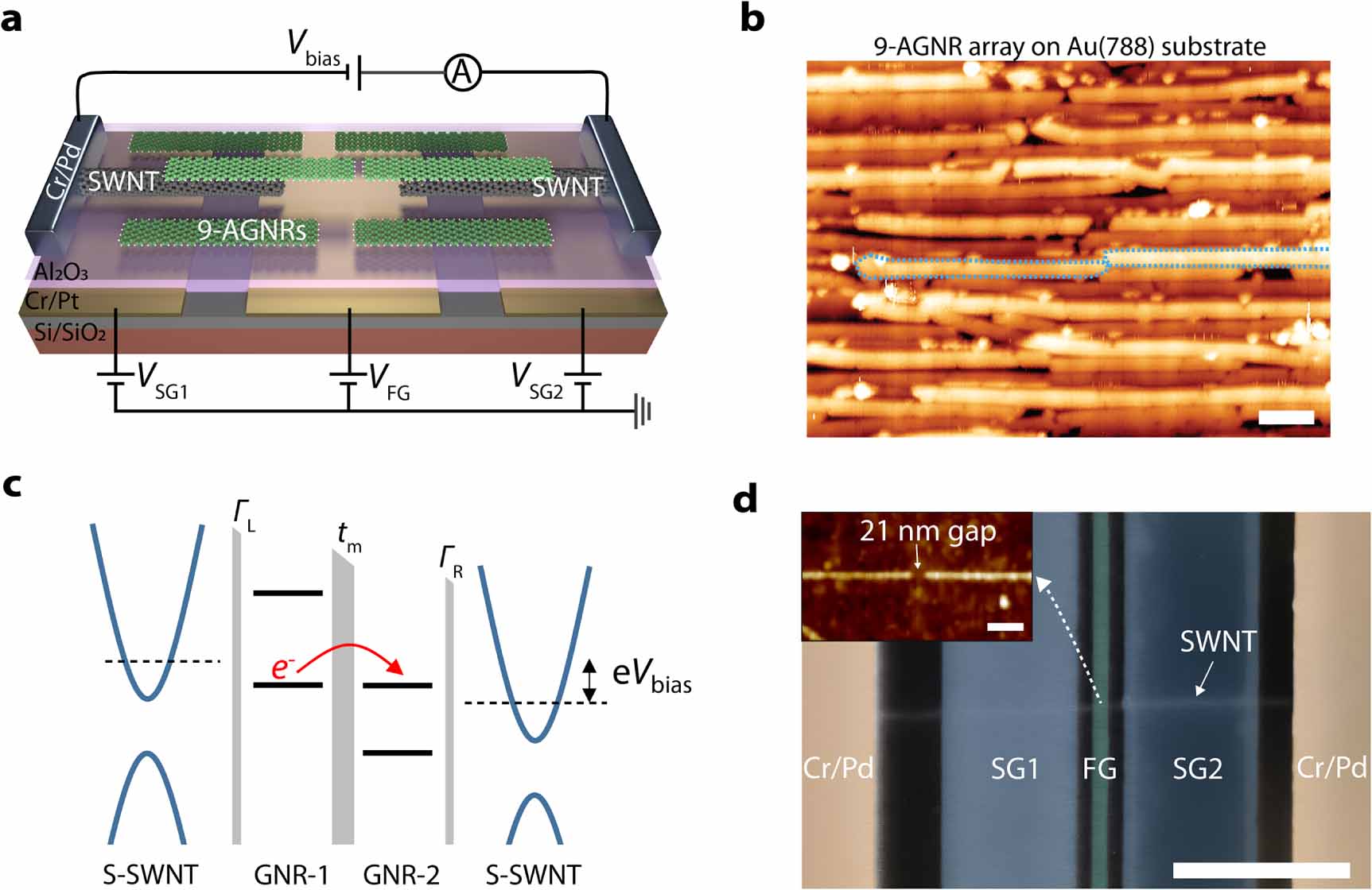
Figure 1. Double QD device from atomically precise GNRs. (a) Device schematic and the measurement circuit. Two serial-connected GNRs are contacted via a pair of SWNT electrodes. Three metal gates are patterned below the SWNT-GNR-SWNT junction and isolated with a 30 nm Al2O3. (b) Scanning tunneling microscopy image of the GNRs on the gold growth substrate, before transfer to the device substrate. The blue dotted lines highlight two GNRs in series. Scale bar, 5 nm. (c) A schematic energy diagram of a double QD made from two serial-connected GNRs contacted by a pair of SWNT electrodes. (d) Scanning electron micrograph of a device similar to the measured device, showing a single SWNT and three bottom gates (SG1, FG and SG2). Scale bar: 1 µm. Inset: topographic AFM image of a representative SWNT nanogap (∼21 nm) located over the FG. Scale bar: 40 nm.
Download figure:
Standard image High-resolution image1. Device fabrication
The device is fabricated on a substrate consisting of highly p-doped Si, covered with 285 nm of thermally grown Si O2. A 100 nm wide and 20 nm thick Cr/Pt FG is patterned alongside the two side gates (SG1 and SG2) and covered by a 30 nm thick Al2O3 layer deposited using atomic layer deposition acting as the gate dielectric. After that, a uniaxially aligned array of single-walled nanotubes (SWNT) is transferred on top of the Al2O3 and individual SWNTs are then contacted by 3/50 nm Cr/Pd electrodes. Then, large nanogaps of 15–25 nm are created in the SWNTs using an optimized electron-beam lithography process in combination with reactive ion etching [11, 15]. Finally, a dense array of uniaxially aligned 9-AGNRs, with lengths of about 45 ± 10 nm [18], is grown on a Au(788) substrate (figure 1(b)) and transferred on top of the device [19] with an array of SWNT electrodes. Our approach critically relies on the self-aligned nature of both the SWNT and GNR growth on their respective growth substrate. Figure 1(d) presents a scanning electron microscopy image of a representative device, with three gates, source/drain contacts, and a single SWNT. A high-resolution atomic force microscope image of the SWNT nanogap is presented as inset, revealing a gap size of ∼21 nm. A detailed description of the fabrication process can be found in figure S1 of the supporting information. Moreover, a similar fabrication process has been reported previously [20].
2. Results and discussion
In a double QD, charges flow through the system when at least one energy level of each dot lies within the bias window, that is, the energy window between the electrochemical potential of the source electrode (µS
) and that of the drain electrode (µD
),  . At zero bias, the levels of the two dots need to be aligned with each other for charges to flow. This alignment can be achieved by adjusting the gate voltage on each QD. In a charge stability diagram recorded on a non-coupled QD in which the voltage on each gate is varied, this leads to a series of points, also called the tripled points, at which charges can flow through the system. When the two dots are coupled by an interdot coupling tm
, these triple points are split by 2tm
, and the well-known hexagonal, honeycomb structure is observed.
. At zero bias, the levels of the two dots need to be aligned with each other for charges to flow. This alignment can be achieved by adjusting the gate voltage on each QD. In a charge stability diagram recorded on a non-coupled QD in which the voltage on each gate is varied, this leads to a series of points, also called the tripled points, at which charges can flow through the system. When the two dots are coupled by an interdot coupling tm
, these triple points are split by 2tm
, and the well-known hexagonal, honeycomb structure is observed.
In case a finite bias voltage is applied, current will also flow when the two levels are not exactly aligned. For this reason, the triple points evolve into bias triangles. The tip of the triangle corresponds to the situation where the level on each dot is aligned with the electrochemical potential of its adjacent electrode. The base of the triangle represents the situation when the two sites are aligned with each other. On one side of the triangle, they align with the electrochemical potential of the source electrode, and on the other side, they align with the drain electrode. The line connecting the tip of the triangle with the center of the base is typically referred to as the detuning axis, along which the two levels gradually move apart from each other at the same rate until they each align with the electrochemical potential of their adjacent electrode [21].
While single-QD devices based on SWNT-GNT-SWNT junctions have been extensively discussed in our previous work [15], in this work we focus on one device where double QDs are formed. This device is electrically characterized at room temperature at different stages during the fabrication process: Before the nanogap formation (the pristine SWNT), after the gap formation and after 9-AGNR transfer. These measurements, provided in figure S2 of the supporting information, are performed in a three-terminal fashion by applying a DC voltage bias on the source electrode, measuring the current at the drain electrode, and applying a voltage on the FG. The degenerately doped Si substrate is grounded. Both the SWNT before patterning and the final SWNT-GNR-SWNT junction show p-type semiconducting properties. As expected, the nanogap exhibits current levels at the noise floor of our setup. As the SWNT behave as p-type semiconductors, their conductance is highly sensitive to the applied gate voltage. To ensure a maximally conducting electrode, both V and V
and V are set below 0 V or sometimes fixed at −4 V, well in the hole-transport (conductive) regime.
The electrical properties of the SWNT-GNR-SWNT device are extensively characterized as a function of the different gate voltages in a Helium-3 refrigerator with a base temperature of 255 mK. In the figure S3 of the supporting information, we show a VBias–VFG conductance map (V = V
= V V) and three I–V characteristics at V
 V, 0 V and 0.5 V. A conductance/bias gap between −200 mV and 200 mV is observed, as well as gate-independent resonances, which we attribute to the presence of states in the leads that are not affected by the side gates. Figure 2(a) plots the current as a function of the voltage applied on FG (VFG) and SG1 (V
 ), measured at V
 mV. In addition, the V
 is set to −4 V to ensure the SWNT electrode is in its conducting state. The current map shows a series of triangles of high current pointing to the left and organized on a grid-like pattern. These features are reminiscent of the honeycomb-like pattern characteristic for charge stability diagrams of double QD systems. In such diagrams, the two gates (FG and SG1) control the number of charges on dot 1 and 2, respectively. While at low bias the corners of the honeycomb correspond to the triple points at which the energy level of the left dot aligns with the energy level of the right dot, these triple points evolve to bias triangles when high bias voltages are applied [21]. In the measurements, bias voltages of ±250 mV are used, where distinct triangles are observed. We find this be an ideal value as for bias voltages between −200 mV and 200 mV, charge is blockade and for larger values, the bias triangles gradually expand, resulting in an increased overlap between adjacent triangles.

Figure 2. Double QDs tuned by FG and SG1. (a) Current as a function of FG voltage and SG1 voltage (charge stability diagram) in the double QD regime at V V and V
 mV. (b) Schematic model of the double QDs with two capacitively coupled gates (FG and SG1). The QDs are coupled to the source (S) and drain (D) electrodes via tunnel junctions. SG2 is set to −4 V. (c) High-resolution measurement zooming in around several bias triangles. (d) Energy level schemes of the double QDs corresponding to the triangle marked by the black solid line in (c). (e) Line-cut along the detuning axis marked by the black dashed line in (c). The red solid line is a Lorentzian fit to the ground state lines of the triangle in (c). (f) High-resolution measurement of a triangle at positive bias VBias = 250 mV.
Download figure:
Standard image High-resolution imageWe attribute these triangles to the formation of double-dots in the nanojunction, as shown by a schematic of a double QD system coupled capacitively to FG and SG1 in figure 2(b). The measurement at positive V does not reveal any further triangles, presumably due to the Fermi energy of the electrodes entering the band gap of the SWNT on top of SG1 electrode. From the size of the area(marked with black dashed lines in figure 2(a), the spacing between the adjacent triangles in FG and SG1 axes is extracted to be ΔVFG = 0.150 V and ΔV
 = 0.091 V, respectively. For extracting additional information, figure 2(c) zooms in on a particular region of large current, highlighting the triangular shape of the triple points. This shape is characteristic of double dot systems. From the size of the representative triangle marked by the thick black lines, we extract the gate couplings, converting gate voltages to energy, and find
  = eV
= eV /δV
/δV eV V−1 and
  = eV
= eV /δV
/δV eV V−1. Using these values, we find addition energies in QD 1 and dot 2 to be 106.5 meV, and 23.7 meV, respectively. The triangle depicted in figure 2(c) is schematically represented in figure 2(d). Along the baseline of the triangle, the ground states of the two dots are aligned and shifted within the bias window. When moving along the detuning axis (black dashed line from the black point to the tip of the triangle), the energy levels in QD 1 shift downward while those in QD 2 shift upward. At the tip of the triangles, the ground states of the two dots are aligned with the Fermi levels of the source electrode and drain electrode, respectively. Along the detuning axis, at the green point, a stepwise increase of the current is observed, which we attribute to the alignment of the ground state of dot 1 with the first excited state of dot 2. At this point, resonant transport leads to a rise in the current. When the ground/excited states of the two QDs are not aligned, charge transport is non-resonant, possibly dominated by inelastic tunneling processes [21]. In figure 2(c), the transition from the nonresonant to resonant transport is observed and marked by a green dashed line. Figure 2(e) plots the current as a function of the detuning energy as marked by the black dashed line in figure 2(c). From the data, the level spacing ΔE
 of dot 1 is extracted to be around 20.3 meV. To determine the tunnel coupling, we further analyze the resonant tunneling data as plotted in figure 2(e). As the measurement temperature is 255 mK ≈ 21.5 µeV, the condition of eVBias
 κbT is fulfilled, and thus the line width of the resonance at zero detuning is temperature independent. To extract the interdot coupling, we fit the current to a double QD model [22, 23] (red curve in figure 2(e)) assuming a Lorentzian line shape leading in the limit of weak interdot tunnel coupling tm

 : Transport through the excited states can be analyzed more quantitatively using the result from Stoof and Nazarov for resonant tunneling [22, 23]. In particular, the inter-dot coupling and coupling to the electrodes can be extracted. In the limit of a weak inter dot tunnel coupling tm

 , the current I follows a Lorentzian line shape as a function of detuning
  :
:

where h is the Plank constant, tm
the interdot tunnel rate and  the tunnel rates to the left and right lead, respectively. Figure 2(e) plots a line-cuts along the detuning axis for negative bias V
 mV. The red line represents a Lorentzian fit for extracting inter-dot coupling and the lead-dot coupling. The fit yields an interdot tunnel coupling of
  meV and a dot-lead tunnel coupling of
  meV.
meV.
Alongside these triangle patterns, many resonances in the vertical direction are observed as shown in figures 2(a) and (c), showing up as small peaks in the linecut shown in figure 2(e). The energy difference  between these resonances is between
  meV. These resonances are attributed to the modulation of the SWNT lead states, which will be discussed in more detail later.
In double QD systems, the sequence in which the charge is flowing through the QDs can be obtained from the shape of the bias triangles, with the tip pointing towards the charge state towards which the charge is flowing. The triangle is therefore bias polarity dependent. figure 2(f) shows a representative triangle measured at a large, opposite (positive) bias VBias = +250 mV. Here, the orientation of the triangle is reversed. Similar to figure 2(e) and marked by a green dashed line , charge transport through an excited state is observed. The level spacing of dot 2 is estimated to be  meV.
meV.
Interestingly, the two QDs can also be tuned using the FG and SG2, while keeping the voltage on SG1 fixed at V V. Figure 3(a) shows a schematic diagram of a double QD system coupled capacitively to FG and SG2. Figure 3(b) plots the current as a function of the VFG and V
 , measured at V
 mV and V
 V. The map shows a similar honeycomb pattern characteristic as that in figure 2(a). The gates FG and SG2 control the number of charges on dot 1 and 2, respectively. Again, from the size of the area (marked by black dashed lines in figure 3(b), the spacing between the adjacent triangles along the FG and SG2 axes is extracted to be ΔVFG = 0.173 V and ΔV
 = 0.21 V, respectively. Figure 3(c) shows a zoom-in triangle enclosed by the red dashed line in figure 3(b) measured at V
 mV. Within this triangle, a resonant line (as marked by green dashed line) parallel to the baseline is observed due to resonant transport through the ground state of QD 2 and excited states of QD 1. Figure 3(d) plots the current as a function of the detuning energy as cut by the black dashed line in figure 3(c). From the data, the level spacing ΔE
 of dot 1 is extracted to be around 18.0 meV in this transport regime. By fitting the resonance at zero detuning using the equation (1), an interdot tunnel coupling of
  meV and a dot-lead tunnel coupling of
  meV are extracted.

Figure 3. Double QDs tuned by FG and SG2. (a) Schematic model of the double QDs with two capacitively coupled gates (FG and SG2). The QDs are coupled to the source (S) and drain (D) electrodes via tunnel junctions. The SG1 is biased with −4 V constantly. (b) Current as a function of FG voltage and SG2 voltage (charge stability diagram) in the double QD regime at V V and V
 mV. (c) Close-up of the triangle marked in the red dashed box in (b). (d) Line-cut along the detuning axis marked by the black dashed line in (c). The red solid line is a Lorentzian fitting to the ground state line of the triangle in (c).
Download figure:
Standard image High-resolution image
We note that for both the charge stability diagrams showed in figures 2 and 3, the current is completely suppressed when VBias
 200 mV and no triple points or bias triangles are measured. This could be caused by the ungated semiconducting SWNT segments between Cr/Pd contacts and SG1/SG2, as shown in figure 1(d), or caused by localized states at the SWNT leads. In this device, the double QDs are formed by two GNRs connected in series, not in a single GNR or involving the SWNT electrodes, for the reasons discussed below. First, many narrow and vertical resonances are observed in the charge stability diagrams (e.g. figures 2(a) and (c)). These resonances are mainly modulated by the SG1, while being almost independent on the FG. Thus, we attribute these vertical narrow resonances to states associated with the SWNT lead states, as the SGs are expected to couple more strongly to the SWNT leads due to its close proximity. Moreover, the energy spacing
  of these vertical resonances is
  meV, which is significantly smaller than the level spacings of
  = 20.3, 38, 18 meV for the double QDs. Given the largely different energy scales, we attribute the QDs to the GNRs and the closely-separated resonances to states present in the SWNT. Second, as the gate coupling αFG is about 3 times larger than
  or
or  , we conclude that both the QDs are located in the nanogap rather than in the leads, located on top of the SGs. Third, the extracted interdot tunnel couplings (
 or 0.049 meV) are much smaller than the dot-lead tunnel couplings (
 or 18 meV), as calculated from the Lorentzian fits in the two charge stability diagrams (figures 2(e) and 3(d). These fits support that the two QDs are formed in two distinct GNRs in series with a large tunneling barrier in between. In addition, the large dot-lead tunnel couplings suggest that the orbital overlap between the states of the leads and those of the electrodes is large, possibly due to a large contact length between the two GNRs and source/drain SWNT electrodes. Finally, lead states in the SWNT electrodes result in additional resonances. We also anticipate that using metallic SWNT as contact electrodes would greatly reduce the presence of such resonances by their continuous density of states around the Fermi energy. This more favorable density of states would prevent the gate electrodes from pinching off the current in the electrode and would allow tuning the double QD in the low-bias regime.
While this study reports on the observation of double QD behavior based on bottom-up synthesized GNRs, several aspects are not ideal in the current implementation. First, the location of the QDs is not well controlled, leading to a significant amount of cross-talk between the two gates. Moreover, applying a voltage on the gate also pinches off the conductance of the electrodes. This renders it challenging to identify the charge state of both dots. Without the presence of a charge sensor, it is therefore challenging to determine the charge state of the system, in particular in the region where the electrodes are switched off. In addition, given the number of electrons on the two GNRs, it is highly unlikely that a full depletion of the two QDs can be achieved in order to reach the  charge state from which it is possible to count the absolute number of electrons on either QDs. Nevertheless, this study provides the first demonstration of using bottom-up synthesized GNRs for the realization of double QD systems.
3. Conclusion
In conclusion, we have realized a double QD device based on bottom-up synthesized GNRs, contacted using SWNT electrodes and creating an SWNT-GNR-GNR-SWNT junction. The device possesses three electrostatic gates with which the double QD system can be tuned and accesses different charge states. At cryogenic temperatures, the measurements exhibit double QD characteristics such as the formation of bias triangles and the presence of excited states. The level spacing of GNR QDs, as well as the interdot tunnel coupling and lead-dot tunnel coupling, are extracted by analyzing the measured triangle features. In addition, the energy of the excited states is determined. As the addition energies in GNRs can be tuned to the range of hundreds of mili-electronvolt range, we envision the realization of double QD systems that operate at non-cryogenic temperatures, with major implications for several quantum technologies that currently heavily rely on mili-Kelvin operation temperatures.
Acknowledgments
M C acknowledge funding by the EC H2020 FET Open Project No. 767187 (QuIET) and by the Swiss National Science Foundation under the Sinergia Grant No. 189924 (Hydronics). M L P acknowledges funding by the Swiss National Science Foundation (SNSF) under the Spark Project No. 196795 and the Eccellenza Professorial Fellowship No. PCEFP2_203663, as well as funding by the Swiss State Secretariat for Education, Research and Innovation (SERI) under Contract Number MB22.00076. G B B, P R and R F acknowledge funding by the Swiss National Science Foundation under Grant No. 200020-182015, the European Union Horizon 2020 research and innovation program under Grant Agreement No. 881603 (GrapheneFlagship Core 3), and the Office of Naval Research BRC Program under the Grant N00014-18-1-2708. We also greatly appreciate the financial support from the Werner Siemens Foundation (CarboQuant). We thank Michael Stiefel and the Cleanroom Operations Team of the Binnig and Rohrer Nanotechnology Center (BRNC) for their help and support.
Data availability statement
All data that support the findings of this study are included within the article (and any supplementary files).
Author contributions
Jian Z, M L P and M C conceived and designed the experiments. K M provided the GNR precursor molecules. G B B under the supervision of P R and R F, performed the on-surface synthesis and substrate transfer of GNRs. L Q under the supervision of Jin Z performed the growth of aligned SWNTs and SWNT transfer. Jian Z, and P C fabricated the devices. Jian Z and M L P performed the electrical measurements. Jian Z and M L P analyzed the data. Jian Z and M L P wrote the manuscript. All authors discussed the results and their implications and commented on the manuscript.
Conflict of interest
The authors declare that they have no competing interests.
Supplementary data (1.6 MB PDF)