
Abstract
We report a numerical design procedure for pursuing a near-unity coupling efficiency in quantum dot (QD)-cavity ridge waveguide single-photon sources (SPSs) by performing simulations with the finite element method. Our optimum design which is based on a 1D nanobeam cavity, achieves a high source efficiency εxy of 97.7% for an isotropic in-plane dipole, together with a remarkable Purcell factor of 38.6. Such a good performance is mainly attributed to the high index contrast of GaAs/SiO2 and a careful cavity design achieving constructive interference and low scattering losses. Furthermore, we analyze the bottleneck of the proposed platform, which is the mode mismatch between the cavity mode and the Bloch mode in the nanobeam. Accordingly, we present the optimization recipe of an arbitrarily high-efficiency on-chip SPS by implementing a taper section, whose high smoothness is beneficial to gradually overcoming the mode mismatch, and therefore leading to a higher Purcell factor and source efficiency. Finally, we see good robustness of the source properties in the taper-nanobeam system under the consideration of realistic fabrication imperfections on the hole variation and QD position deviation.
Export citation and abstract BibTeX RIS

Original content from this work may be used under the terms of the Creative Commons Attribution 4.0 license. Any further distribution of this work must maintain attribution to the author(s) and the title of the work, journal citation and DOI.
1. Introduction
A deterministic and high-quality single-photon source (SPS) has a great potential to become an indispensable building block in numerous applications ranging from quantum computing [1–3], quantum cryptography [4–6] to large-scale on-chip quantum information processing [7–10]. The semiconductor quantum dot (QD)-based scheme features a wide operational range, on-demand photon generation, good stability, and compatibility with on-chip technology [7, 8, 11], making it outstanding from the many candidates. However, the QD emission in bulk material has no directional preference, leading to an extremely low collection efficiency of less than 1% in free space [12]. Employing a nanostructure and engineering a cavity around the QD allows the guidance of photon propagation and boosts the coupling efficiency into a single guided mode thanks to Purcell-enhanced spontaneous emission (SE) [13–17]. State-of-the-art micropillar [14], and photonic crystal (PC) waveguide cavities [18–22], can offer a near-unity source efficiency. However, PC-based sources suffer from poor out-coupling into single-mode waveguides, which is a limitation towards large-scale integration [23]. On the other hand, the rotationally symmetric property of the micropillar SPS results in an equal excitation on two polarization orientations. Thus, the extraction efficiency meets the 50% bottleneck after the post-filter operation under the resonant excitation strategy [24]. This can be avoided by implementing the stimulated biexciton cascade decay [25] or breaking the symmetry in the elliptical micropillar [15, 24].
A more straightforward way to simultaneously avoid these drawbacks is to embed the QD into a semiconductor ridge waveguide, which features low propagation loss [26, 27] and selective guidance of photons with specific polarization orientation [28]. Applying this strategy, the coupling efficiency from an InAs QD to a bare GaAs ridge waveguide located on the top of a low index silica substrate has achieved  % [28]. Recently, researchers presented a rectangular distributed Bragg reflector (DBR) holes-based SPS featuring an efficiency of 86% [29], and a value of 73% in a circular-hole DBR device [30]. Nevertheless, realizing a near-unity efficiency comparable to the state-of-the-art micropillar or PC waveguide SPS in semiconductor ridge waveguide platform is still of critical importance and under pursuit. One possible solution is the tapered cavity, which can help to reduce the losses into radiation via an adiabatic transition from fundamental cavity mode to Bragg mirror mode [31, 32], and thus can be fused into the ridge waveguide SPS design to approach the source efficiency that we are pursuing.
In this work, we numerically investigate the SE rate and source extraction efficiency of the InAs QD-GaAs cavity waveguide coupling system on a SiO2 chip. We tailor the waveguide dimensions to only support the propagation of the fundamental transverse electric (TE) mode and naturally suppress the transverse magnetic polarization. Thanks to the Purcell effect introduced by the carefully-designed cavity, the directional improvement in power funneled into the waveguide fundamental TE mode leads to a near-unity source efficiency comparable to the state-of-the-art. Moreover, our platform shows good tolerance to some potential realistic fabrication imperfections. Overall, we propose an optimization recipe to achieve arbitrarily high efficiency in the QD-nanobeam cavity waveguide platform.
2. General concept
The structure under consideration in this work is schematically depicted in figure 1. An infinitely long GaAs ridge waveguide surrounded by air is on the top of a substrate with a lower index material SiO2. The inset of figure 1 shows the fundamental TE mode, denoted by mode M, is well confined inside the structure instead of leaking into the substrate, mainly thanks to the significant index contrast between GaAs and SiO2. An InAs QD with the free-space emission wavelength of 940 nm is embedded on the central axis of the waveguide. We build a cavity composed of two sets of DBRs formed by cylindrical air holes around the QD to improve its SE rate with the help of the Purcell effect. Considering SE wavelength, the refractive indexes are set as  ,
,  , and
, and  [28]. We adopt a finite element method (FEM) based commercial solver (JCMsuite [33]) and the usage of HPC cluster hardware [34] to perform fully three-dimensional numerical simulations in this work. The self-assembled semiconductor QD typically features a several times larger horizontal than a vertical extension, and thus can be modeled as a linear in-plane xy-polarized dipole under the consideration of the dipole approximation [33, 35, 36]. The red double-headed arrow in figure 1 depicts the orientation of an xy-polarized dipole. θ is the polarization angle, randomly distributed in the xy-plane. Since one can always project the arrow onto two base axes, we consider the total emission from the sum of two cases: purely x-polarized (θ = 0) and purely y-polarized (
 ) dipoles.
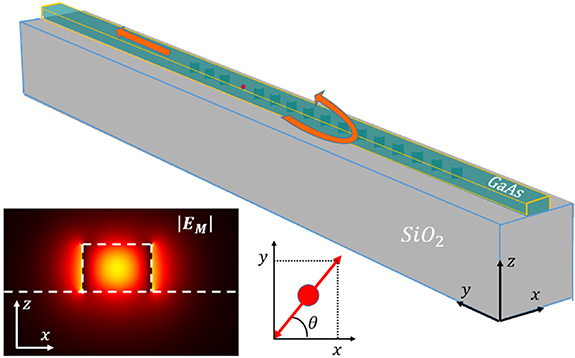
Figure 1. Sketch of the GaAs nanobeam cavity waveguide on top of the SiO2 substrate. An InAs quantum dot denoted by the red circle is embedded in the center of the cavity sandwiched between two mirrors formed by cylindrical air holes. The red double-headed arrow represents the dipole orientation, which can always be projected onto two base axes x and y. The curved arrow indicates most of the light going to the bottom mirror is reflected back to the cavity, and this part escapes from the top mirror along with the light emitting upwards, as demonstrated by the straight arrow. Inset is the 2D mode profile of the fundamental TE mode M propagating along the bare ridge waveguide.
Download figure:
Standard image High-resolution imageCorrespondingly, we define  as the power emitted by the
  -polarization configuration. The Purcell effect describes the enhancement of the QD SE rate by the nanostructure. The Purcell factor can quantify this effect and is defined as:

where P0 is the power emitted by the QD in the bulk material. As the figure of merit, the coupling efficiency of an xy-polarized dipole is given by [37]:

where  denotes the power emitted by the
  -polarized dipole funneled into the mode M and is evaluated by the overlap of the scattered electromagnetic field and the mode M at the waveguide cross-section, which is pointed by the arrow in figure 1. When the dipole is on the central axis of the waveguide, it always yields
  [28, 37]. Therefore, we simplify the notation in the following by
  only referring to
  . We also investigate the efficiency of the source only under the x-polarized configuration, defined as:

From the aspect of the numerical simulations in JCMsuite, we use the following solvers for solving different categories of problems in the whole work: a propagation mode solver for computing waveguide modes, a mode solver for computing Bloch modes for the cylindrical air hole unit cell, a scattering solver for computing scattered field with a dipole excitation and deducing Purcell factor, and a mode solver for computing the modes of the full structure and deducing Q factor [33].
3. Designs and results
3.1. QD coupled to a ridge waveguide
First, we investigate the dependence of εxy
on the waveguide geometry for an infinitely long and pristine waveguide (with no holes), whose cross-section and top view are depicted in figures 2(a) and (b). We consider a rigde waveguide of height h and width w in the ranges ![$h\in[100\, \mathrm{nm},300\, \mathrm{nm}]$](https://content.cld.iop.org/journals/2633-4356/2/4/045004/revision3/mqtaca8e8ieqn13.gif) ,
, ![$w\in[200\, \mathrm{nm},580\,\mathrm{nm}]$](https://content.cld.iop.org/journals/2633-4356/2/4/045004/revision3/mqtaca8e8ieqn14.gif) respectively, with a step-size
respectively, with a step-size  nm. Transparent boundary conditions are implemented using perfectly matched layers [33] to perform the infinitely spatial scattering simulations. Then, we compute the mode overlap and the emitted power by
  -polarized dipole for each set of parameters to calculate the Purcell factors and efficiencies according to equations (1)–(3), and the results are shown in figures 2(c)–(g). The white areas correspond to the specific sets where no guided mode can be found.

Figure 2. (a), (b) Front view/top view of the QD-bare ridge waveguide system with physical dimensions: w = waveguide width, h = height, and material properties: substrate SiO2 (dark blue), waveguide GaAs (yellow), embedded QD (red cross).  denotes the power emitted by x-polarized dipole into the fundamental propagation mode M. In this bare waveguide, two opposite arrows indicate two equal output channels. (c), (d) Purcell factors
  for
for  -polarized dipole, (e) mode coupling power
  normalized by its maximum value, and (f), (g) coupling efficiencies
  for
for  -polarized dipole as functions of waveguide width and height. The white cross represents the physical dimensions yielding the optimum efficiency.
Download figure:
Standard image High-resolution imageComparing figures 2(c) and (d), the Purcell factor of y-polarized dipole Fy
is more sensitive to the dimensional variation than that of x-polarized dipole Fx
. This is because the oscillation axis of the y-polarized emitter (y-axis) is perpendicular to the waveguide cross-section (xz-plane) [37]. Next, we consider the sum of the power extracted from the top and bottom outputs,  and
and  , as shown by the arrows in figure 2(b). In principle,
  =
=  +
+ . Figure 2(e) shows
  normalized by its maximum value.
  increases by reducing the waveguide dimensions to an optimum mode confinement.For a purely x-polarized emitter, the coupling efficiency εx
can reach as high as 95%. In addition, the area with a small cross-sectional size can maintain high efficiency of over 90%, as shown in the dark-red area in figure 2(f), where we can also see εx
diagonally drops, as indicated by the arrow. The reason is that a wider structure supports additional guided modes, thus decreasing the relative emission into the fundamental TE mode. The white cross in figure 2(g) represents the geometric parameters h = 140 nm and w = 220 nm yielding a maximum coupling efficiency εxy
of 70% for an xy-polarized emitter. The structures that we investigate in the following will inherit this set of dimensions.
increases by reducing the waveguide dimensions to an optimum mode confinement.For a purely x-polarized emitter, the coupling efficiency εx
can reach as high as 95%. In addition, the area with a small cross-sectional size can maintain high efficiency of over 90%, as shown in the dark-red area in figure 2(f), where we can also see εx
diagonally drops, as indicated by the arrow. The reason is that a wider structure supports additional guided modes, thus decreasing the relative emission into the fundamental TE mode. The white cross in figure 2(g) represents the geometric parameters h = 140 nm and w = 220 nm yielding a maximum coupling efficiency εxy
of 70% for an xy-polarized emitter. The structures that we investigate in the following will inherit this set of dimensions.
Comparing figures 2(d), (f) and (g), higher values of εxy
coincide with high εx
and low Fy
. Moreover, the bright/dark areas in figure 2(g) almost perfectly correspond to the dark/bright areas in figure 2(d). This is due to  and the strong dependence of efficiencies on the dipole orientation (x). Therefore, the distribution of εxy
relies on the interplay of εx
and Fy
, and a relative suppression of Fy
will significantly contribute to a higher εxy
. However, a bare waveguide always features
and the strong dependence of efficiencies on the dipole orientation (x). Therefore, the distribution of εxy
relies on the interplay of εx
and Fy
, and a relative suppression of Fy
will significantly contribute to a higher εxy
. However, a bare waveguide always features  , which means we will always lose 50% of the light if we only collect from the top. Therefore, in the following we will try to make
  by engineering a highly reflective bottom mirror.
3.2. Design concept and results for a DBR in a ridge waveguide
As depicted in figure 3(a), the DBR mirror is composed of cylindrical air holes with a number of  . The hole radius r and the distance between successive hole centers, periodicity ph
, should be carefully selected to ensure a good reflection from the bottom mirror at the designed SE wavelength 940 nm. We find the correct periodicity by performing a photonic band structure calculation for 3D unit cell of the PC in a 1D-periodic arrangement for different values of ph
and r, as shown in the inset of figure 3(b). The yellow shade indicates the bandgap [38] of the periodic structure with parameters r = 20 nm,
. The hole radius r and the distance between successive hole centers, periodicity ph
, should be carefully selected to ensure a good reflection from the bottom mirror at the designed SE wavelength 940 nm. We find the correct periodicity by performing a photonic band structure calculation for 3D unit cell of the PC in a 1D-periodic arrangement for different values of ph
and r, as shown in the inset of figure 3(b). The yellow shade indicates the bandgap [38] of the periodic structure with parameters r = 20 nm,  nm, in the center of which a red dashed line denotes its center wavelength
  precisely at 940 nm. For the highest possible reflectivity in DBR, the band gap should be engineered exactly around the SE frequency. After scanning the periodicities for three radii that we would investigate in the following and extracting all the corresponding center wavelengths, we finally get the impact of ph
on
precisely at 940 nm. For the highest possible reflectivity in DBR, the band gap should be engineered exactly around the SE frequency. After scanning the periodicities for three radii that we would investigate in the following and extracting all the corresponding center wavelengths, we finally get the impact of ph
on  , as shown in figure 3(b). It reveals that a longer period is necessary for a larger hole or a longer wavelength to achieve the greatest reflection. The intersections of the dashed lines in figure 3(b) represent the optimal ph
of three periodic structures at the designed wavelength 940 nm. They are
, as shown in figure 3(b). It reveals that a longer period is necessary for a larger hole or a longer wavelength to achieve the greatest reflection. The intersections of the dashed lines in figure 3(b) represent the optimal ph
of three periodic structures at the designed wavelength 940 nm. They are  , respectively. By applying these parameters, we can expect a fairly high bottom reflection to appear in this structure.
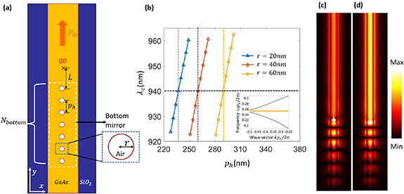
Figure 3. (a) Top view of the QD-ridge waveguide system with bottom mirror, formed by an array of periodic and uniform holes.  denotes the number of holes in the bottom mirror, L and ph
is the distance from QD to the bottom mirror and between two adjacent periods. Inset shows the enlarged view of one of the air holes with the radius of r. Emitted photons can only propagate through one output channel, as the arrow indicates. (b) Center wavelength λc
, obtained from the bandgap calculation of three different hole radii (r = 20 nm, r = 40 nm, r = 60 nm), as a function of periodicity ph
. The intersections of horizontal and vertical dashed lines imply three suitable ph
to reach
denotes the number of holes in the bottom mirror, L and ph
is the distance from QD to the bottom mirror and between two adjacent periods. Inset shows the enlarged view of one of the air holes with the radius of r. Emitted photons can only propagate through one output channel, as the arrow indicates. (b) Center wavelength λc
, obtained from the bandgap calculation of three different hole radii (r = 20 nm, r = 40 nm, r = 60 nm), as a function of periodicity ph
. The intersections of horizontal and vertical dashed lines imply three suitable ph
to reach  nm (designed wavelength). Inset shows the bandgap (yellow shade) of a period with r = 20 nm,
  nm, where the red dashed line indicates the center frequency (
 nm). (c), (d) Field profile
  when QD is at a random position/an antinode relative to the bottom mirror under the same color bar.
Download figure:
Standard image High-resolution imageNext, a stronger Purcell enhancement can be achieved by the constructive interference between the forward-propagating photons and the ones reflected at the bottom mirror [37], which requires the dipole to be precisely at an antinode relative to the mirror. We first place the emitter at a random distance L to the bottom mirror to obtain a field profile, where we can observe the position of the antinodes. As shown in figure 3(c), there are three antinodes between the dipole and the mirror, indicated by three bright standing wave patterns. The second step is to choose one of the antinodes and relocate the emitter there. Here, we avoid the first antinode in case there is any influence induced by the close distance between QD and DBR. In this structure, we choose the third antinode to locate the dipole, and the field profile is shown in figure 3(d), where the output signal is much stronger than that in figure 3(c). As mentioned above, this results from a perfect constructive interference when the emitter is precisely at the antinode. The quantitative analysis for the dipole misalignment will be discussed in section 3.4. For different radii, the distances of QD to the bottom mirror used in this work are given as follow: 
 . Although we observed an enhanced SE rate and
  by only implementing a bottom mirror, we are still pursuing a better Purcell factor and higher source efficiency, as shown in the next section.
3.3. QD in nanobeam cavities with and without taper
The third step in the design procedure is to construct a complete cavity, in which two sets of DBR sandwich the QD in the center, and thus cavity length is twice as long as L. By applying the parameters designed in the previous step, the cavity will further enhance the QD SE through a more substantial Purcell effect. Figure 4(a) is the sketch of a QD-nanobeam cavity waveguide coupling system. Here, we design a top mirror with a higher transmission than the bottom one, which is achieved by using less holes. For a purely x-polarized dipole, part of the total emitted power  funnels into the waveguide fundamental guided mode M, denoted by
  . The rest lost into radiation, named
  , mainly appears at the interfaces of the cavity and the DBRs.
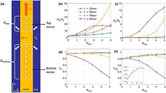
Figure 4. (a) Top view of the QD-nanobeam cavity waveguide (regular DBR) coupling system.  is the number of periods in top/bottom mirror. For x-polarized dipole,
  denotes the power funneled into fundamental mode M, all the other power lost by radiation
  is depicted by the small arrows, total power
  . (b), (c) Emitted/lost power
  and (d), (e) coupling efficiencies
  for
for  -polarized dipole as a function of
  . Inset shows the maximum efficiency εxy
can reach 97.7% with parameters: r = 20 nm,
. Inset shows the maximum efficiency εxy
can reach 97.7% with parameters: r = 20 nm,  .
.
Download figure:
Standard image High-resolution imageFigures 4(b)–(e) show the impact of the number of periods in top mirror  on the SE properties and coupling efficiencies under four sets of configurations. Generally, when
  increases, the top reflectivity increases as well. For each data point,
  is accordingly increased to ensure the bottom reflectivity stays higher. Here, we state that the parameters used in the design of r = 30 nm are
  nm, L = 291 nm. Figure 4(b) demonstrates the normalized
  emitted by an x-polarized dipole as a function of
  . In the range of
 ![$N_\mathrm {top}\in[0,5]$](https://content.cld.iop.org/journals/2633-4356/2/4/045004/revision3/mqtaca8e8ieqn55.gif) , the large size design (r = 60 nm) has already reached the highest Purcell factor. In contrast, the curves for 20, 30 and 40 nm are still going up but will not increase infinitely. Due to the scattering taking place at the cavity-DBR interface, there is a trade-off between the enhancing quality factor and the scattering loss when increasing
, the large size design (r = 60 nm) has already reached the highest Purcell factor. In contrast, the curves for 20, 30 and 40 nm are still going up but will not increase infinitely. Due to the scattering taking place at the cavity-DBR interface, there is a trade-off between the enhancing quality factor and the scattering loss when increasing  , and therefore those curves will reach a maximum at a larger
  . As
. As  increases, the reflectivity from the top becomes comparable to that from the bottom, and thus more light into the free space leads to a rise in
  , as shown in figure 4(c). Here, the structure with the smallest size (r = 20 nm) yields the lowest
  . Figures 4(d) and (e) confirm indeed that a smaller radius is beneficial for suppressing
  , as both εx
and εxy
achieve much higher values in this regime.
, as both εx
and εxy
achieve much higher values in this regime.
We find a maximum efficiency εxy
= 97.7% for r = 20 nm and  (and a corresponding
  ), accompanied by a Purcell factor of
  , and a Q factor of 668. As the supplementary information to figure 4(e), we show the maximum efficiency εxy
for four different radii and the corresponding period configurations in table 1. The optimum efficiency increases with a smaller hole radius thanks to the reduction in scattering losses. Still, it pays a cost for more periods due to the reduced reflection from a single hole. A single computation in the parameter scan is performed with an accuracy setting yielding an estimated numerical relative error of
, and a Q factor of 668. As the supplementary information to figure 4(e), we show the maximum efficiency εxy
for four different radii and the corresponding period configurations in table 1. The optimum efficiency increases with a smaller hole radius thanks to the reduction in scattering losses. Still, it pays a cost for more periods due to the reduced reflection from a single hole. A single computation in the parameter scan is performed with an accuracy setting yielding an estimated numerical relative error of  for Q and of
  for εxy
. The corresponding discrete problem has a dimension of N = 14 836 908 and is solved on with a RAM consumption of 500GB and with a computation time of roughly 4 hours, using 6 nodes on a standard workstation. The numerical error has been estimated using a numerical convergence study with gradually increasing numerical accuracy settings.
for εxy
. The corresponding discrete problem has a dimension of N = 14 836 908 and is solved on with a RAM consumption of 500GB and with a computation time of roughly 4 hours, using 6 nodes on a standard workstation. The numerical error has been estimated using a numerical convergence study with gradually increasing numerical accuracy settings.
Table 1. Maximum coupling efficiency εxy under different configurations.
| Radius (nm) |

|

| Maximum εxy |
|---|---|---|---|
| 20 | 85 | 12 |

|
| 30 | 35 | 5 |

|
| 40 | 15 | 3 |

|
| 60 | 10 | 1 |

|
To make a more fabrication-friendly design, the last step in the design procedure is to find a structure with fewer periods but which can keep a near-unity coupling efficiency simultaneously. On one hand, the r = 20 nm platform effectively suppresses the scattering loss into the free space but takes a large number of periods because a single period contributes very little to the overall reflectivity. On the other hand, the 40 nm platform achieves high bottom reflection with few holes, but features stronger scattering losses due to a significant mode mismatch between the Bloch mode in the DBR mirror section and the cavity mode. One way to take advantage of both configurations is to implement a taper section [39–41] in the bottom mirror, where the hole radius gradually increases from 20 nm in the vicinity of the QD to 40 nm. We thus consider a bottom mirror consisting of  holes of radius 40 nm and a taper section including
  holes, as shown in figure 5(a), and the new variable distance between two holes pʹ is given by
  , where
  and
and  are the individual periodicities of two adjacent periods. The principal power loss in this platform still appears at the interfaces of the cavity and two mirrors, as depicted by the thick arrows.
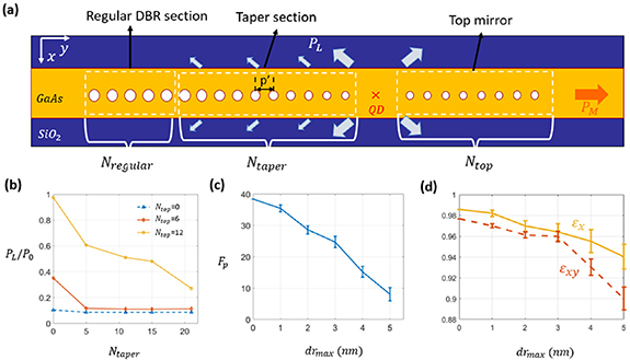
Figure 5. (a) Top view of the QD- taper cavity waveguide structure. The bottom mirror is divided into a taper section and a regular DBR section, whose number of holes are described by  and
and  . (b) Power into radiation modes
  as a function of
  . (c) Purcell factor for x-polarized dipole and (d) coupling efficiencies
  for
for  -polarized dipole as a function of maximum radius deviation
  from the perfectly designed holes in the entire structure. All the data shown in (c) and (d) are obtained from 10-times simulations.
Download figure:
Standard image High-resolution imageHowever, the increased size in the taper section also introduces additional scattering loss, denoted by the small arrows in figure 5(a). We investigate the impact of  on the normalized
  , as shown in figure 5(b). We can find increasing
  will effectively suppress
  . In our investigations, the cavity effect is indispensable, and therefore we employ a large
  in the design. Then, we propose an optimum new design yielding a coupling efficiency
  , a remarkable Purcell factor of 38.3, and a Q factor of 616 with the parameters
  ,
,  ,
,  . Compared with the previous result in this section, which is obtained via 20 nm-hole regular DBR nanobeam cavity, we achieve identical performance but with only 1/3 of the total periods in the bottom mirror, contributing to a smaller mode volume and, in turn, a broader bandwidth.
In principle, the figure of merit εxy can be further improved by using a longer taper section and smaller holes, but these come at the price of much longer structure and heavier calculations. Under the premise that the minimum design radius is 20 nm, we do not implement a similar taper section in the top mirror and instead keep the regular DRB. This avoids the additional power loss introduced by the increased radius in the taper.
3.4. Investigation of the impact of fabrication tolerances on the performance of the SPS
Considering the imperfections that will appear in the actual situations, the tolerance study for the optimum QD-taper cavity platform is carried out by randomly changing the radii of the well-designed holes. Figures 5(c) and (d) demonstrate the Purcell factor and efficiencies as a function of the maximum radius deviation  between the designed radii and the possible imperfections in fabrication, which means that each hole radius is changed by an individual random amount in the interval (0,
  ). Even under a 5 nm deviation, our platform is still robust on εx
and εxy
, keeping the performances of over 90% with a standard deviation of 1%. However, the Purcell factor is more sensitive to imperfect situations. This is because a misalignment of the new antinode with respect to QD position leads to poor constructive interference.
). Even under a 5 nm deviation, our platform is still robust on εx
and εxy
, keeping the performances of over 90% with a standard deviation of 1%. However, the Purcell factor is more sensitive to imperfect situations. This is because a misalignment of the new antinode with respect to QD position leads to poor constructive interference.
In section 3.2, the field strength comparison between figures 3(c) and (d) implies the QD-cavity coupling might highly depend on the accuracy of the QD position. To offer a more quantitative analysis, we investigate the impact of QD misalignment on the SPS performance. In this subsection, we still consider the on-axis dipole but change its position along the axis. We define ρ as the deviation of QD position from the ideal center in the cavity, and this value varies in the range [−(L−rb ),(L−rt )] when we assume ρ = 0 is the cavity center. Here, L is the half cavity length, and rb (rt ) is the radius of the hole closest to the cavity in the bottom (top) mirror. The peaks and valleys in figure 6(a) correspond to the QD at the cavity's antinodes and nodes. The wave shape is the consequence of walking in the cycle between constructive and destructive interference. The green shade area reveals that a relative QD position deviation of 50 nm is tolerable with a cost of 50% Purcell enhancement. In figure 6(b), the efficiencies εx and εxy present an even broader spatial linewidth, denoted by the blue shade area. Within a 90 nm QD-cavity center deviation, our platform can still perform a more than 90% coupling efficiency.

Figure 6. (a) Purcell factor for x-polarized dipole and (b) coupling efficiencies  for
for  -polarized dipole as a function of ρ, which is the deviation of on-axis QD (red cross) from ideal cavity center (green dot). The shade areas indicate the tolerance ranges of the QD-taper cavity waveguide SPS on the imperfect QD position.
Download figure:
Standard image High-resolution image
4. Conclusion
In summary, we adopt the FEM to numerically investigate the QD SE and its coupling efficiency to the waveguide fundamental guided mode in a nanobeam cavity SPS. A careful cavity design can not only improve the dipole emission but also boost the source efficiency via lower scattering losses. By investigating the impact of the hole radius on the dipole emission properties, we find that the smaller the hole, the better it controls the scattering loss at the cavity-DBRs interfaces and that in the taper. Our optimum platform appears with a near-unity efficiency (97.7%), a remarkable Purcell factor of 38.6, and a Q factor of 668. We also propose a taper to strongly reduce the number of holes in the bottom mirror by a factor of  , and to achieve a broader bandwidth, corresponding to a slightly lower Q factor of 616. Moreover, the Purcell factor and efficiency are still comparable to those in the optimum system. Considering the feasibility in fabrication, the smallest hole applied in the current design is with a radius of 20 nm. However, it is possible to pursue a source efficiency arbitrarily close to unity by reducing the radii in the overall structure and increasing the number of holes in the taper section based on our design. Finally, the platform under investigation is proven tolerant of imperfections on the hole variation and QD position deviation, especially for source efficiency. To some extent, our work is promising to allow for the fabrication of the nanobeam SPS with significantly improved performance compared to today, and provide the potential contribution to the integrated on-chip, and large-scale quantum information processing.
Acknowledgments
The authors acknowledge support from the European Research Council (ERC-CoG 'UNITY', Grant 865230), from the European Union's Horizon 2020 Research and Innovation Programme under the Marie Sklodowska-Curie Grant Agreement No. 861097, from the Independent Research Fund Denmark (Grant DFF-9041-00046B), and from the EMPIR programme co-financed by the Participating States and by the European Union's Horizon 2020 research and innovation programme (Project 20FUN05 'SEQUME').
Data availability statement
The data that support the findings of this study are available upon reasonable request from the authors.