

Abstract
We studied the temperature dependent transport properties and memory behaviour of ultrathin black phosphorus field-effect transistors. The devices show electrical conductance and field-effect mobility that decreases with the rising temperature. The field effect mobility, which depends also on the gate voltage sweep range, is 283 cm2V−1s−1 at 150 K and reduces to 33 cm2V−1s−1 at 340 K, when the voltage gate sweep range is  50 V. The transfer characteristics show a hysteresis width that increases with the temperature and is exploited to enable non-volatile memories with a wider programming window at higher temperatures.
Export citation and abstract BibTeX RIS

Original content from this work may be used under the terms of the Creative Commons Attribution 4.0 licence. Any further distribution of this work must maintain attribution to the author(s) and the title of the work, journal citation and DOI.
Introduction
Two-dimensional (2D) materials, in monolayers or a few-layer form, have attracted significant attention for high-scalable and low-power electronic devices [1–5]. Specifically, few-layered black phosphorus (BP) exhibits higher mobility and a more tunable band gap (0.3−2 eV) in comparison to other 2D semiconducting materials [6–8]. These characteristics of BP establish it to be critical in novel devices for optoelectronics [9, 10], non-volatile memories [11, 12], photovoltaics [13], and field-effect transistor (FET) [14, 15] applications.
Thus, due to the continuously targeted applications of BP, the understanding of its electrical transport mechanisms, mainly in terms of various physical parameters such as temperature, pressure, and environments, is of great value to confirm thermal stability, phase transformation, etc. It has been found that, at higher pressure, BP goes through a series of phase transitions and becomes superconductive [16–18], indicating that correlated phenomena play an important role under extreme conditions. On the other hand, due to the chemically active atoms at edges or defect sites, BP tends to attract chemisorbed species and results in instability. The stability of BP after chemical modifications such as hydrogenation, fluorination, and oxidation [19], and the tensile strength improvement due to Ar gas absorption [20] have been studied.
The electrical properties of BP at different temperatures are yet the subject of intense research. However, there are few reports related to the thermoelectric (TE) properties of BP. For instance, TE measurements of BP have been investigated in the temperature (T) range of 77−300 K and it was found that the Seebeck coefficient (S) of BP is lower than 0.1 mV/K for a thickness in the range of 5−100 nm [9, 21]. Further, it has been found that S of bulk BP reaches 0.3−0.4 mV/K for T in the range of 300−400 K [22]. In another report, in a hexagonal boron nitride (h-BN—BP—h-BN) sandwiched configuration, it has been reported that carrier transport at low temperatures is facilitated, due to the Shubnikov−de Haas oscillations and a quantum Hall effect with Landau level filling factors down to two in conventional laboratory magnetic fields [23]. Further, ohmic contact with vacuum annealing below 250 °C exhibits improved current-voltage characteristics, while at the temperature over 300 °C, the device performance deteriorated after vacuum annealing due to the catalytic amorphization of BP caused by the metal electrode [24]. Temperature dependent processing has been widely used as an approach for improving structural defects [25], ohmic contacts [26], as well as cleaning the thin film for microelectronic applications. This can effectively reduce the contact resistance [27] and eliminate residues adsorbed on the surface of the channel layer in 2D thin film based electronic devices [28], improving the electrical performance and long-term stability. Since, BP is vulnerable to ambient molecules, especially at higher temperatures, thermal annealing in the vacuum can be an effective method to measure the actual performance of the devices. However, systematic studies of the dependence of the electrical transport properties on the temperature are still lacking.
Recently, BP has shown some notable performance for memory applications. Mostly reported non-volatile memories based on 2D materials employ a charge-trapping layer or heterojunctions to collect and store the charges induced by the applied gate voltage. H. Tian et al studied a BP/Al2O3 based memory device, demonstrating the existence of four different memory states and, hence, 2-bit per cell data storage [29]. Grillo et al exploited the BP and SiO2 defects without an additional charge-trapping layer for the realization of stable non-volatile memory performance longer than 200 cycles [12]. Zhang et al demonstrated a BP/h-BN/graphene heterostructure in which BP acts as a transport channel layer, hexagonal boron nitride (h-BN) serves as a tunnel barrier layer, and graphene as a charge-trapping layer, resulting in two different operating modes [30]. Lee et al showed that Au nanoparticles can be employed as a charge-trapping layer for mechanically exfoliated few-layered BP FETs enabling a large memory window of about 60 V [11]. Recently, Huang et al demonstrated a BP/MoS2 heterojunction with a record-high on/off current ratio as a memristor [31]. Wang et al demonstrated POx/BP memristor with reliable resistive switching, long data retention time, and repeatable programmable behavior. They reported that the resistive switching originates from the oxygen vacancy migration in the self-assembled grown phosphorous oxide layer [32].
Here, we fabricated back-gated BP FETs by directly transferring exfoliated BP flakes onto a pre-defined SiO2/p++ Si substrate. We then systematically investigated the charge carrier transport in the temperature range between 150–340 K, in the dark, and low-vacuum. As expected, we found that characteristic electrical parameters of the transistor, such as on/off current, hysteresis width, and mobility, are strongly sensitive to temperature. We explain such behaviour in terms of charge traps at the BP/SiO2 interface and phonon scattering mechanism. Moreover, we also report BP channel-based temperature dependent stable non-volatile memory performance and a wider programming window.
Experimental methods
Multilayers BP thin flakes were mechanically exfoliated by adhesive tape from the bulk BP single crystals (from Smart Elements). A standard photolithography process followed by electron beam evaporation was used to deposit 10 nm Ni/70 nm Au electrodes. Prior to the electrical measurements, the BP channel-based device was dipped in acetone and isopropanol to remove the protective poly(methyl methacrylate) (PMMA) layer. The fabricated BP devices were back gated with silver (Ag) pastes onto the degenerate Si substrate. A detailed explanation of the device fabrication procedure can be found elsewhere [12]. Figures 1(a), (b) show the schematic diagram, and the optical image of a typical BP transistor, with channel length and width of 5.2 μm and 13.3 μm, respectively, that were used for the analysis. Atomic force microscopy (AFM) measurements were performed, and the obtained height profile of the flakes is about 30 nm, as depicted in the inset of figure 1(b).

Figure 1. (a) Schematic diagram, and (b) the optical image of the fabricated BP transistor (the inset represents the height profile along the dotted white line obtained by AFM).
Download figure:
Standard image High-resolution imageThe electrical measurements were performed in the two-probe configuration using a Janis ST-500 probe station connected to a Keithley 4200 SCS (semiconductor characterization system), having current and voltage sensitivity of about 0.1 pA, and 2 μV, respectively. All the electrical measurements were carried out at 2 mbar pressure and different temperatures. The substrate temperature was monitored using a Scientific Instruments Model 9700 temperature controller, and the chamber pressure was maintained using a Pfeiffer Vacuum pump.
Results and discussion
Initially, the general behaviour of the device was analysed by transfer (Id-Vgs, drain current as a function of gate voltage) and output (Id-Vds, drain current as a function of source-drain voltage) characteristics at room temperature. Figure 2(a) displays the output characteristics measured for −10 mV ≤ Vds ≤ 10 mV and Vgs stepping from −50 V to + 50 V, at room temperature, and pressure of 2 mbar. The linear behaviour points to good ohmic contacts [33, 34]. This is consistent with the reduction of the Schottky barrier height for increasing BP thickness reported by Jiang et al who found a vanishing Schottky barrier height for Cr contacts over BP with more than 10 layers [35]. We did not observe any change in the linear behaviour at the various gate voltages, confirming the presence of good ohmic contacts. Next, the higher channel current for negative gate bias indicates that p-type charge carriers are present in the device. Figure 2(b) represents the transfer characteristics of the device obtained at room temperature by measuring Id as a function of different sweeping gate voltages, up to −50 V ≤ Vgs ≤ 50 V, at a constant drain bias, Vds = 2 mV. The device exhibits a unipolar, p-type behaviour and hysteresis related to the charge/discharge of intrinsic and interfacial traps between BP channel and SiO2 [36–39]. Figure 2(c) demonstrates that the hysteresis width Hw, defined as the Vgs difference corresponding to the average current Im = (Ion + Ioff)/2, between the highest (Ion) and lowest (Ioff) currents at the extreme of the Vgs range, as depicted in figure 2(b), is a growing function of Vgs. The enhancement in Hw as a function of the gate voltage range indicates that charge storage occurs across the SiO2 capacitor. We exclude a dominant role of adsorbates in the obtained hysteresis as measurements were performed in the vacuum [28, 37]. Figure 2(d) shows Ion and Ioff currents extracted from the transfer characteristics of the BP device over the investigated Vgs range, highlighting a current modulation factor of about 5. Our findings of the on/off ratio around 5 are consistent with the reported literature. L Feng et al fabricated devices with BP flakes with a thickness ranging from 6 to 50 nm and studied the dependence of the transistors on the material's thickness. They found that the drain current increases by several orders of magnitude for thickness increasing from 6 to 20 nm, while only a few times increases are observed for thicknesses over 20 nm [40]. F Xia et al investigated the dependence of BP based transistors on the thickness. They reported an exponentially decreasing on/off current ratio for BP flakes ranging from 2 to 17 nm [7]. Likewise, H Liu et al reported a decreasing on/off ratio with increasing crystal thickness, which becomes less than 10 for BP thicknesses higher than 15 nm [41].

Figure 2. (a) Output characteristics, (b) transfer characteristics, (c) hysteresis width, (d) Ion and Ioff current values, and (e) extracted mobility of the BP device.
Download figure:
Standard image High-resolution imageCharge carrier mobility of the BP film was calculated using the following equation
where L and W are the channel length and width, respectively, and dId/dVgs is the maximum slope of the transfer curve.
Figure 2(e) depicts the calculated two-terminal field-effect hole mobilities, in the reverse and forward bias direction, with maximum values of 95 and 120 cm2V−1s−1 at Vds = 2 mV, respectively. The different mobilities in the two directions and the dependence on Vgs are due to the interfacial trap states which are differently populated and show different behaviour for the two gate-voltage sweeping directions. We note that the observed hole mobility is higher than in our previously reported work on thin BP [12] at room temperature. This could be due to less defective BP flake in the present case. However, the obtained mobility is lower than in other recently reported works where the mobility was measured on thinner flakes [35, 40]. Indeed, it has been shown that BP mobility decreases with increasing thickness [41]. This trend has been further confirmed by Feng et al that reported a rapid increase in mobility below the BP thickness of 21.7 nm [40]. Furthermore, Jiang et al reported a mobility of 521 cm2V−1s−1 but for a thinner BP FET of 6 nm [35]. We also remark that the mobility decreases with increasing Vgs sweep range because more carriers are trapped at the BP/SiO2 interface at higher Vgs.
Figure 3(a) shows the temperature dependence of the electric behaviour of the device in the 150 − 340 K range, at Vds = 2 mV and Vgs in the range ± 50 V. The device maintains its unipolar p-type conductance behaviour. We found that the conductance decreases, while the hysteresis width increases, with the increasing temperature. The hysteresis width of around 40 V at 340 K is about two orders of magnitude higher than at 150 K, where it is 0.4 V (see figure 3(b)). This indicates temperature-enhanced trapping at the BP/SiO2 interface because the high temperature might facilitate the charge trapping at the BP/SiO2 interface. The obtained Ion and Ioff currents decrease as the temperature increases. The highest current is more than 7 μA at T = 150 K and reduces to about 1.3 μA at T = 340 K. This is a very promising result for low temperature electronic applications.
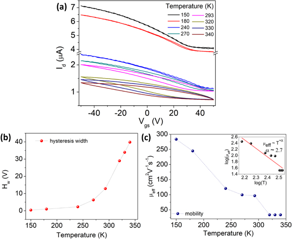
Figure 3. (a) Temperature dependent transfer characteristics, (b) transfer width, and (c) forward mobility of the BP device.
Download figure:
Standard image High-resolution imageAdditionally, the carrier mobility reduces as the temperature increases, and this is consistent with the current trend. Figure 3(c) shows the calculated field effect mobility from the forward sweep slopes of the transfer characteristics of the device at different temperatures. The mobility passes from about 283 cm2V−1s−1 at T = 150 K to 33 cm2V−1s−1 at T = 340 K. This characteristic could be understood by the fact that the mobility is influenced by two types of scattering mechanisms, (i) from charged impurities and (ii) from phonons. Charged impurities' scattering is typically only seen at very low temperatures. In the temperature range we examined, the phonon scattering is dominant, and the mobility is expected to decrease with temperature following a power law, μeff ∼ T−α , where α is a positive number that can be measured experimentally. For the atomically thin 2D materials, in a similar temperature range, the exponent α has been reported to be ranging from 1 to 6 for graphene [42–45], ∼ 2 for GeAs [46] , ∼ 1.7 for MoS2 [47]. In the present case, a fit of the data of figure 3(c) yields α ∼ 2.7 (see inset figure 3(c)).
Figure 4(a) shows the transient behaviour of the device at different temperatures. The current is monitored during a series of Vgs = ± 30 V pulses applied to the gate.

Figure 4. (a) Temperature dependent memory performance, (b) transfer characteristics, and (c) memory programming window of the fabricated BP FET.
Download figure:
Standard image High-resolution image
A positive or a negative Vgs pulse sets the current at a given level, which evolves with time, exhibiting similar behaviour at different temperatures. The separation between the two different current states, obtained with positive and negative Vgs, is retained for a time longer than 40 s, indicating a non-volatile behaviour. Figure 4(b) displays the corresponding transfer curves highlighting the widening hysteresis for increasing temperatures. This trend is reflected in the memory behaviour. At zero gate voltage applied for memory read purposes, the two currents (erase and program states, see inset figure 4(c)) are more separated at higher temperatures, passing from 1.3 μA at 293 K to 6.8 μA at 340 K (figure 4(c)). This provides us with a wider memory programming window at higher temperatures. The good data retention characteristic may be attributed to the long BP/SiO2 interface trapping. In fact, there are several defects formed at the BP/SiO2 interface that provide deep intragap states acting as trap centers. These trap centers are caused by adsorbates, or process residues at the BP/SiO2 interface and charged ions in the SiO2 layer. Charge carriers can be stored by these trap centers under the effect of the gate voltage. Trapping and detrapping occur mainly by tunneling but factors such as temperature can also influence the trapped charge density. The shape of the transfer characteristic, which tends to have a right shift for increasing Vgs sweeping range (see figure 2(b)), indicates accumulation of negative charge. When the gate pulse is in the high positive or negative state, the drain current increases or decreases rapidly, and intragap trap states get filled or emptied by electrons, causing the memory effect.
Thus, BP based FETs can be considered as a potential device for non-volatile memories which can function over a wide temperature range, as requested for example in automobiles.
Conclusions
In conclusion, we fabricated and investigated the temperature dependent behaviour of unipolar p-type FETs based on a BP channel. FET mobility was observed to increase at low temperature, reaching a value of about 283 cm2V−1s−1 at 150K. It was observed that at higher temperatures the carrier mobility is limited by phonon scattering. Further, a stable memory response of the device and wider memory programming window at higher temperatures was reported. This study provides a better understanding of BP properties and their dependence on temperature and suggests pathways for non-volatile memory usage.
Data availability statement
The data cannot be made publicly available upon publication because they are not available in a format that is sufficiently accessible or reusable by other researchers. The data that support the findings of this study are available upon reasonable request from the authors.
Author declarations
The authors have no conflicts to disclose.
Funding
This research was funded by the University of Salerno, Italy, grant numbers ORSA218189 and ORSA223384. A.D.B. and A.K. acknowledge the European Union's REACT-EU PON Research and Innovation 2014–2020, Italian Ministerial Decree 1062/2021 Project. M.S., S.S., and O.K. acknowledge financial support from the DFG within the SFB 1242 ('Non-Equilibrium Dynamics of Condensed Matter in the Time Domain') Project C5, #278 162 697).