
Abstract
Electric fields play a crucial role in modulating the electronic properties of nanoscale materials. Electron emission, induced by an electric field, is a representative phenomenon. Experimental and theoretical aspects of such electron emission from graphene are briefly reviewed. The emission occurs at the edge of graphene flakes, not at the surface, because the edge highly concentrates the electric field. Emission currents are sensitive to the edge shapes and edge functionalization. This review provides guiding principles for designing high-efficiency field-emission devices by using graphene nanostructures.
Export citation and abstract BibTeX RIS

Original content from this work may be used under the terms of the Creative Commons Attribution 4.0 licence. Any further distribution of this work must maintain attribution to the author(s) and the title of the work, journal citation and DOI.
1. Introduction
Electrons in matter are basically bound via deep attractive potentials of their constituent nuclei. Electrons are occasionally emitted to outside matter by applying appropriate external conditions to matter. An external electric field, the thermal effect, or photoirradiation causes electron emission from matter; known as field, thermal, photoelectron, Schottky, and ballistic emissions. Among these emission mechanisms, electron emission that is induced by the electric field (i.e., field emission (FE)) is an active area of research in the pure and applied sciences because of the fast turn-on process, low working temperatures, and ultrahigh brightness [1, 2]. In addition, the thermal emission also has been widely studied due to their importance in both vacuum and solid-state devices [3, 4]. Accordingly, FE is widely applicable to modern technologies; such as displays [5–8], lithography [9, 10], x-ray tubes [11–13], and electron microscopes [14, 15]. In FE, electrons of the cathode material pass through the material surface into vacuum by overcoming the electrostatic barrier, under an external electric field on the order of 10∼100 MV/cm. Such a strong field enables electron tunneling from bound states in the matter near the Fermi level to the vacuum outside the matter, in accordance with the modulation of the potential profile outside the matter (figure 1).
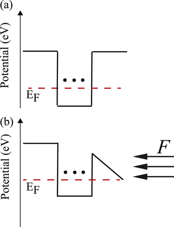
Figure 1. Change of potential profile of matter under an external electric field. The potential of matter (a) without an electric field and (b) under an electric field. The black dots in the potential well indicate the atomic positions of matter.
Download figure:
Standard image High-resolution imageThe FE current I is described in terms of an applied electric field (F) by the Fowler–Nordheim (F–N) theory:


where a = 1.54 × 10⁻⁶ A·eV/V2, b = 6.83 × 10⁹ eV−3/2 · V/m, β is the field enhancement factor at the material surface, ϕ is the work function of the emission site of the material, and m is the slope of the F–N plot (obtained by plotting  versus 1/F, which determines the field-enhancement factor) [16]. This conventional F–N theory was derived from planar emitters under an assumption that electron dispersion in material is a parabolic type function. Therefore, many field emission experiments on graphene nanostructures have reported that current–voltage characteristics of graphene do not well agree with the conventional F–N law [17–20]. To overcome the problem, Ang et al proposed a generalized electron emission model, which can describe the field emission from two-dimensional materials with unusual electronic structures [21]. This formula indicates that the emission current depends on the electric field, field enhancement factor, and work function of the surface of the cathode materials. For an efficient field emitter, a high current density at a low electric field is desirable. Therefore, the field enhancement factor should be as high as possible and the work function ϕ as low as possible. In addition, the field screening effect and FE stability are also important factors for determining the FE efficiency. For instance, the field screening effect associated with the proximity of emission sites substantially decreases the electric field around the emission sites, leading to the decrease of the emission current [22]. Finally, for obtaining a stable FE current, the cathode material should be chemically and thermally stable, with high thermal and electric conductivity.
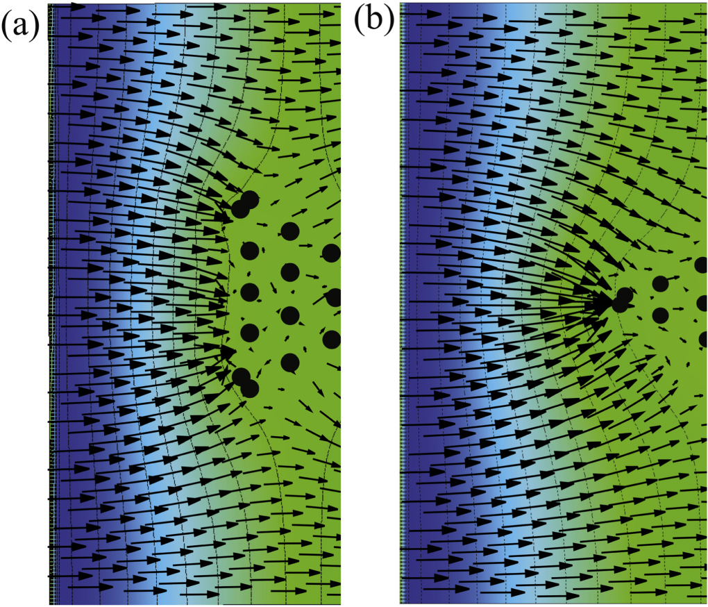
The electric field is highly concentrated at the sharp region rather than the flat region of materials according to the electromagnetism, even though the materials have nano-scale structures (figure 2) [23]. For instance, the electric field is highly concentrated at the tips of carbon nanotubes and metal nanostructures, resulting in a high emission current and bright emission patterns [21, 24–29]. Atomistic images have been observed from field emitters comprising single- and multi-walled carbon nanotubes, enabling researchers to detect the details of atomic structures of their tips [25, 26, 30–34]. Graphene is a promising material for field emitters because of its unique structures and useful properties [20, 35–41]. The atomic thickness of graphene results in a large aspect ratio, which leads to a high enhancement factor that decreases the turn-on electric field. Furthermore, the mechanical and chemical stability renders graphene a stable FE source. A strong covalent network of sp2 C atoms ensures suppressed degradation of the structure, a high electronic conductance ensures a high current density, and a high thermal conductance brings faster dissipation of heat [42, 43]. Accordingly, a number of theoretical and experimental efforts have focused on uncovering the physics behind the FE phenomena of graphene and improving its FE efficiency to advance its wide application. Here, experimental and theoretical aspects of the FE of graphene and its nanostructures are reviewed.
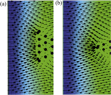
Figure 2. Electric field concentration around a nano-scale material. Vector plots of electric field distributions at the (a) flat and (b) sharp regions of a diamond nanowire.
Download figure:
Standard image High-resolution image2. Electronic structure of graphene and its nanostructures
Electron emission of graphene reflects its electronic structure near the Fermi level. Firstly, the electronic structures of graphene and its nanostructures are briefly reviewed. Because of a hexagonal bipertite network of sp2 C atoms, graphene has a pair of linear dispersion bands at the Fermi level, and at the K point, in the two-dimensional Brillouin zone [44–46]. By introducing imperfections, the hexagonal bipertite structure renders graphene a unique material for band engineering at the Fermi level. Atomic vacancies and nanopores cause non-bonding π electron states at the Fermi level, leading to spin polarization around the imperfections and long-range spin ordering through graphene nanostructures [47–49]. Edges causes peculiar edge-localized states (edge states) (figure 3(a)), which are attributable to the delicate balance in the electron transfer near the edge atomic sites when the edges have a zigzag shape [50–54]. In contrast, graphene nanoribbons with armchair edges are semiconductors, in which the band gap asymptotically decreases and oscillates with increasing width (figure 3(b)) [51, 55–59]. Furthermore, the electronic structure near the Fermi level also exhibits interesting variations, depending on the edge chiral angles [60, 61].

Figure 3. (a) Band structure and edge states of graphene nanoribbons with zigzag edges. Reproduced with permission from [50]. © [1996] The Physical Society of Japan. (b) Energy gaps of graphene nanoribbons with armchair edges at k = 0 and zigzag edges at k = 2π/3, as a function of the ribbon width W [56].
Download figure:
Standard image High-resolution imageThe electronic structure of graphene nanoflakes also strongly depends on their geometric structures: Triangular flakes possessing armchair edges have finite energy gaps between bonding and antibonding states, whose gap energies gradually decrease with the increase of the flake size. In contrast, triangular flakes with zigzag edges, known as [n]traiangulene (n is the number of hexagons along it edge), exhibit peculiar electronic structure: Non-bonding states emerge at zero energy or Fermi level, whose number exactly corresponds with the number difference of two sublattices in their hexagonal networks [62, 63].
Edge functionalization of graphene highly modulates the electronic structure near the Fermi level, which causes unique electron states that depend on the functional groups [64]. The planar structure of graphene can enable formation of a thin film structure where the stacking arrangement is tunable. The electronic structure of the thin film is sensitive to the stacking arrangement [65–68]. Bilayer graphene with a twisted stacking arrangement at a particular small angle exhibits superconductivity because of the flat band (attributable to the band repulsion in the folded small Brillouin zone) [66], even though bilayer graphene with an AB stacking arrangement has a pair of parabolic bands at the Fermi level. Therefore, graphene and its nanostructures are promising materials which are used to explore unusual electron emission phenomena, because of such materials unique intrinsic electronic structures at and near the Fermi level.
3. Experimental works on the FE from graphene and its nanostructures
Because of its planar structure with structural and morphological variations, graphene has various emission sites under an electric field. By constructing nanostructures from graphene, edges, wrinkles, and flat surfaces are potential emission sites. Xiao et al studied the FE of individual single-layer nanostructured graphene adsorbed onto SiO2. They constructed edges, wrinkles, and flat areas by scratching graphene on SiO2 with an anode probe (figures 4(a) and (b)). FE current from the lifted edge was larger than that from the surface or an edge that was attached to the substrate [36]. Thus, the free-standing edges were preferential sites of electron emission under an electric field. In contrast, emission from the surface of graphene required a high turn-on field, even though a stable emission current was observed. Highly efficient and stable FE with a turn-on field of 0.5 V/μm at 1μA was observed in 3-nm-thick graphene oxide sheets lying on the vertically aligned Ni nanotip arrays (figure 4(c)) [69]. Similarly, the effect of graphene on the field emission of InP nanocrystals arrays was also investigated. The FE was improved, when graphene was covered on the InP nanocrystals arrays, due to higher conductivity of graphene as well as the formation of additional ripples and edges on graphene lying on the arrays [70]. A FE current with a turn-on electric field of 600 V/μm at a current of 10 pA was observed from single- and few-layer graphene flakes transferred onto SiO2 (figure 4(d)) [71].

Figure 4. (a) Scanning electron microscope image and (b) three-dimensional schematic of curved graphene for field-emission (FE) measurements. FE measurements were performed on points A–E. Reproduced with permission from [36]. Copyright 2010, American Chemical Society. (c) FE current from the surface of graphene oxide sheets supported on Ni nanotip arrays as a function of the applied voltage. Reproduced with permission from [69]. Copyright 2012, American Chemical Society. (d) FE current from the surface of graphene, with various distances between the graphene and anode, as a function of the applied voltage. Reproduced with permission from [71]. Copyright 2011, American Institute of Physics.
Download figure:
Standard image High-resolution imageThe morphology, arrangement, and atomistic structure of graphene depend on its synthesis and affect its FE properties. Radio-frequency plasma-enhanced chemical vapor deposition facilitates preparation of mono- and few-layer graphene vertically aligned with the substrates. Because of the substrate-free edges of single- and few-layer graphene, these systems exhibit remarkable emission properties, with a low turn-on field of 4.7 V/μm (figure 5(a)) [72]. Furthermore, chemical functionalization and coating of graphene can help one to modulate the FE properties of graphene. Hou et al fabricated carbon nanosheets with a thickness of 1–2nm, standing on p-type Si wafers. They found that coatings of CrO2 modulated the emission properties. The turn-on electric field from 4.25 V/μm of as-grown carbon nanosheets was improved to 2.4 V/μm when the nanosheets had a 1.5-nm CrO2 coating (figure 5(b)) [73]. In addition, the atomistic structure or purity of graphene also affects the emission properties. Malesevic et al synthesized few-layer graphene (four to six layers of graphene), aligned vertically to either a Si or Ti substrate, by microwave plasma-enhanced chemical vapor deposition with CH4 and H2. The emission properties depended on the gas concentrations and substrate. An increased H2 concentration improved the emission properties by increasing the field enhancement factor by up to 7500, because H2 causes sharp edges by removing amorphous carbon. In addition, a graphene film on the Ti substrate had a lower turn-on electric field than that on the Si substrate, which was attributable to the superior electrical conductivity of Ti [39].
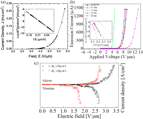
Figure 5. (a) Field-emission (FE) current from nanosheets grown on an Si substrate as a function of the electric field. Inset: corresponding F–N plot. Reproduced with permission from [72]. Copyright 2004, American Institute of Physics. (b) FE current of as-grown graphene sheets and graphene nanosheets coated with CrO2 (at coating thicknesses of 0.5, 1.5, 15, and 20 nm) as a function of the electric field. Inset: corresponding F–N plot. Reproduced with permission from [73]. Copyright 2008, American Institute of Physics [73]. (c) FE current of few-layer graphene grown on Si and on Ti substrates, and synthesized at H2/CH4 gas ratios of 8/1 and 4/1. Reproduced with permission from [39]. Copyright 2008, American Institute of Physics.
Download figure:
Standard image High-resolution imageDoping of foreign elements also affects the emission properties [17, 19, 74, 75]. Palnitkar et al reported that B- and N-doped few-layer graphene exhibited a remarkably low turn-on field of 0.8 and 0.6 V/μm, respectively, at an emission current density of 10μA/cm2 (figure 6(a)). The FE patterns and stability of the emission current were also confirmed (figure 6(b)). The excellent FE was attributed to the high electrical conductivity caused by doping and resonance tunneling [17]. Similar improvements to the FE properties caused by N-doping were also reported in few-layer graphene nanoflakes on bare Si substrates, in which the turn-on field was dramatically reduced to 1.05 V/μm from 1.9 V/μm; the stable FE current lasted for 3 h [19]. The turn-on electric fields of field emitters in these works are listed on table 1.

Figure 6. (a) Field-emission (FE) current as a function of the applied electric field of non-, boron-, and nitrogen-doped graphene. (b) FE current stability of non-, boron-, and nitrogen-doped graphene. Insets: corresponding FE patterns. Reproduced with permission from [17]. Copyright 2010, American Institute of Physics.
Download figure:
Standard image High-resolution imageTable 1. The turn-on electric field (FON ) of graphene nanostructures. Most of them is @ 10 μA/cm2 emission current density.
| Material | FON (V/μm) | References |
|---|---|---|
| Graphene oxide sheet lying on the Ni nanotip Arrays | 0.5 @ 1 μA | [69] |
| Graphene lying on the InP nanocrystal Arrays | 100 @ 10−5 μA | [70] |
| Single and few-layer graphene lying on the SiO2 substrate | 600 @ 10−5 μA | [71] |
| Mono- and few-layer graphene flakes standing on the Si substrate | 4.7 | [72] |
| Carbon nanosheets standing on the Si wafer | 4.25 | [73] |
| Cabon nanosheet coated by CrO2 standing on the Si wafer | 2.4 | [73] |
| Few-layer graphene standing on the Ti substrate | 1 | [39] |
| B-doped few-layer graphene standing on the Si substrate | 0.8 | [17] |
| N-doped few-layer graphene standing on the Si substrate | 0.6 | [17] |
| Few-layer graphene nanoflakes standing on the Si wafer | 1.9 | [19] |
| N-doped few-layer graphene flakes standing on the Si substrate | 1.05 | [19] |
Transfer technique also plays an important role in fabricating field emitters. Recently, Komlenok et al proposed a laser-induced forward transfer technique, which enables crumpled graphene flakes to transfer on a variety of substrates without losing the quality of the initially synthesized. The transferred crumpled-graphene field emitter shows a field enhancement factor of 3300 [76].
The emission patterns generated on a counter screen are important to the investigation of atomic structures of graphene edges. Tsai et al studied the emission patterns from individual, free-standing graphene. Single-layer graphene produces a dot emission pattern (figure 7(a)), indicating that electron emission only occurs at a particular atomic site at the edges, whereas multilayer graphene produces an emission pattern with parallel curved shapes and contrast nonuniformity (figure 7(b)). Tsai et al also confirmed occurrence of the field screening effect by observing the FE pattern from a three-layer graphene sheet, where a line of lower-intensity dots was sandwiched by two parallel lines; indicating that the field at the center layer was screened by electrons in the outermost layers [37]. In addition, the emission pattern reflects the electronic structure of the edge. Saito et al reported the emission pattern from a graphene edge. The pattern consisted of an array of oval spots that were parallel to each other. Furthermore, each stripe was divided into two wings by a central dark line (figure 7(c)). They hypothesized that each oval spot originated from the π orbital of one C atom. Therefore, the dark line resulted from the interference of electron waves from two lobes of π-orbitals, with a phase difference on either side of the graphene plane. The oval shape of each spot was attributed to the anisotropy of the magnification in the directions perpendicular to a graphene plane and parallel to the graphene edge [2]. Furthermore, the emission pattern is sensitive to the graphene edge morphology and termination. There were bright spots on the pattern, after the adsorption of residual gas molecules during the FE (figures 7(c)–(d)) [77]. However, the striped pattern of graphene was unclear when the edge was closed, because of Joule heating during the FE (figures 7(e)–(f)) [78].

Figure 7. Field emission (FE) patterns from a (a) single- and (b) multi-layer graphene emitter (point S: highest emission site; point W: weak emission line pattern). Reproduced with permission from [37]. Copyright 2012, WILEY-VCH Verlag GmbH & Co. KGaA, Weinheim. FE patterns from graphene (c) at the beginning of FE and (d) after FE, at an emission current of 25μA. Reproduced with permission from [77]. Copyright 2016, John Wiley & Sons, Ltd. FE pattern from graphene (e) before and (f) after adsorption of a residual gas molecule. Reproduced with permission from [78]. Copyright 2012, The Japan Society of Applied Physics.
Download figure:
Standard image High-resolution image4. Theoretical works on FE from graphene and its nanostructures
Quantum mechanical calculations provide theoretical insight into the FE of graphene and related materials. Density functional theory (DFT) and time-dependent density functional theory (TDDFT) are powerful tools for unraveling the corresponding physics, and providing guiding principles for designing high-performance FE devices [79–84]. In addition, recently, another quantum mechanical model for simulating FE was developed based on the Bardeen transfer Hamiltonian considering the atomic structure of the emitting material and its quantum properties [85].
The FE from armchair and zigzag graphene nanoribbons was investigated by TDDFT. The time-dependent emission current was evaluated by taking the time evolution of the wave functions of graphene nanoribbons under an electric field. The FE current from a clean zigzag ribbon was larger than that from an H-terminated ribbon; the interpretation of these results was that dangling-bond states contribute to the FE, because of the corresponding reactions with the electric field (figures 8(a) and (b)) [82, 86]. As revealed by experiments, pristine graphene surfaces are not responsible for the FE [36]. However, vacancy defects substantially enhance the emission current by 22 times compared with pristine graphene surfaces, because the unsaturated bonds that are associated with the vacancy are sensitive to the external electric field (figures 8(c) and (d)) [86].

Figure 8. Energy distribution of the field-emission (FE) current for (a) H-terminated and (b) clean zigzag ribbons. On the right-hand side of each panel, the electronic distributions that caused the peaks are shown as blue clouds with C atoms (white spheres) and H atoms (white dots). The dotted and solid lines denote the results in a parallel and perpendicular electric field, respectively. FE images of graphene (c) without and (d) with a vacancy defect. Reproduced with permission from [86]. Copyright 2004, American Physical Society.
Download figure:
Standard image High-resolution imageStatic DFT [87–92] calculations in combination with the F–N formula can also provide the FE properties of various nano-scale materials under an electric field. This procedure can be used to investigate the FE properties of large-scale structures compared with TDDFT approaches. Therefore, detailed edge shape dependence of the FE current can be obtained using this procedure. For instance, the FE current density strongly depends on the edge angles of graphene (figure 9) [93]. The armchair edge has a lower electrostatic potential barrier, such that there is a larger emission current than from the other edge shapes for both clean and hydrogenated edges (figures 9(c) and (d)). For chiral graphene nanoribbons, the electron emission is primarily from the zigzag portion of the edges because of the concentration of electrons by the dangling bond and edge states. The edge hydrogenation substantially enhances the current density for all edge shapes (figure 9(d)). The hydrogenation causes the dipole at the edge atomic sites, which decreases the electrostatic potential barrier outside the edges [93]. Note that the emission current may depend on the temperature when it is high enough to cause the bond dissociation and reconstructions, because the emission current strongly depends on the edge morphology.

Figure 9. Geometries in a unit cell of (a) clean and (b) hydrogenated graphene nanoribbons; with edge angles of 0°, 8°, 16°, 23°, and 30°. FE current as a function of the electric field for (c) clean and (c) hydrogenated graphene nanoribbons. Inset: corresponding F–N plot. Reproduced from [93]. Copyright 2018, Authors.
Download figure:
Standard image High-resolution imageIn addition to the edge shapes, edge functionalization also affects the emission current density. The emission current strongly depends on the functional groups as well as the edge shape and electric field. For both armchair and zigzag edges, H, OH, and COOH groups cause a larger current density than the other functional groups, because these functional groups substantially suppress the electrostatic potential barriers outside the graphene. In contrast, edges with O termination have lower emission currents compared with the other functionalized edges, because of their higher electrostatic potential barriers outside the edge of graphene. The edges functionalized with NH groups exhibit unusual behavior, whereby the NH group enhances the FE current from the zigzag edge but suppresses that from the armchair edge, because the dipole moment of the NH in the zigzag edge is stronger than that in the armchair edge, which arises from the conformational difference of the NH groups at the armchair and zigzag edges (figures 10(a) and (b)). The emission pattern as simulated by the local density of states near the Fermi level strongly depends on the functional groups (figure 10(c)) [94].

Figure 10. Geometries and field emission current densities as functions of the external electric field of functionalized (a) armchair and (b) zigzag graphene nanoribbons. Reproduced with permission from [94]. Copyright 2018, Elsevier Ltd. (c) Contour plots of the local density of states of functionalized zigzag graphene nanorribons by OH, H, O, CHO, COOH, and NH functional groups.
Download figure:
Standard image High-resolution imageEdge morphological effects have also been investigated by DFT with the F–N formula. Stacked graphene nanoribbons with 0.5-nm spacing give the largest current density, whereas the current is insensitive to the ribbon spacing when the spacing is 1 nm or more, for hydrogenated armchair and zigzag edges. In contrast, the current increases with increasing interlayer spacing for clean armchair and zigzag edges (figure 11(a)) [95]. In addition to the open graphene edges, the closed edge of multilayered graphene has been observed during the FE process by transmission electron microscopy [78]. One can enhance the emission current density by closing the edges of bilayer graphene. In particular, for graphene nanoribbons with zigzag edges, the current from the closed edges is remarkably higher than that from the open edges, because the edge closing substantially decreases the electrostatic potential barrier outside the graphene edges (figure 11(b)) [96].

Figure 11. (a) Geometry and field emission (FE) current of graphene nanoribbon arrays, with an interlayer distance of Dx , as a function of the interlayer distance Dx . Reproduced with permission from [95]. Copyright 2005, American Physical Society. (b) Geometries and FE current of bilayer graphene, with closed armchair and zigzag morphologies, as a function of the electric field. Reproduced with permission from [96]. Copyright 2019, Elsevier Ltd.
Download figure:
Standard image High-resolution image
5. Conclusion
This manuscript is a short review of the physical phenomena of the electron emission from the graphene nanostructures. Graphene is a promising material for field emitters because of its unique structures and useful properties. Experimental works have demonstrated that the free-standing edges of graphene are preferential sites for electron emission by applying an electric field. The emission patterns also indicate that the emission occurs at graphene edges. Furthermore, the emission depends on the atomistic structure of graphene nanostructures, which is attributable to the synthesis conditions. Surface and edge coatings by foreign materials also affect the emission properties. Theoretical approaches based on DFT provide theoretical insight into the physical mechanisms of FE from graphene edges. The emission currents from the graphene edges depend on the edge shapes and edge functionalization, because the edge shape and functional groups at the edges substantially affect the electrostatic potential outside the graphene flakes. Furthermore, the edge morphology also affects the emission current: closed graphene edges correspond to a higher emission current than open edges, although closed edges have a lower aspect ratio than open edges. Because graphene has much structural variation, further investigations will reveal new and interesting phenomena, and advance the applications of graphene nanostructures for electron emission devices.
Acknowledgments
This work was supported by JST-CREST (Grant Number JPMJCR1715) from the Japan Science and Technology Agency; JSPS KAKENHI (Grant Numbers JP21H05233, JP21H05232, JP20H05664, JP20K22323, JP20K05253, JP20H02080, JP20H00316, and JP17H01069) from the Japan Society for the Promotion of Science; and the Joint Research Program on Zero-Emission Energy Research, Institute of Advanced Energy, Kyoto University. Part of the calculations was performed on an NEC SX-Aurora at the Cybermedia Center at Osaka University.
Data availability statement
No new data were created or analysed in this study.