
Abstract
Hf0.5Zr0.5O2 (HZO) is an appropriate material for the back-end-of-line (BEOL) process in fabricating ferroelectric TiN/HZO/TiN devices because of its excellent conformality on 3D nanostructures and a suitable crystallization temperature (≥ 350 °C–400 °C). However, in the semiconductor industry, the deposition temperature of TiN is usually higher than 400 °C. Therefore, it is necessary to study the ferroelectric properties of TiN/HZO/TiN devices when the deposition temperature of the TiN top electrode is higher than the HZO film crystallization temperature. In this study, 10-nm-thick TiN top electrodes were deposited at various temperatures on the HZO thin film to investigate the impact of the TiN deposition temperature on the structural features and ferroelectric properties of TiN/HZO/TiN capacitors. Only the sample capped with a TiN top electrode deposited at 400 °C showed ferroelectric properties without subsequent annealing (in situ crystallization). However, this sample exhibited an approximately 40% reduction in the polarization value compared with the other samples that were crystallized after the annealing process. This behavior can be ascribed to the formation of a monoclinic nonpolar phase. To prevent the degradation of the polarization value and suppress the formation of the m-phase in the in situ crystallized HZO thin film, a two-step TiN deposition method was carried out. The sample was fabricated by depositing a 5-nm-thick TiN top electrode at room temperature followed by the deposition of a 5-nm-thick TiN layer at 400 °C, which resulted in strong ferroelectric properties comparable to those of the samples capped with TiN grown at relatively low temperatures (room temperature, 200 °C, and 300 °C). These findings can adequately explain the role of the capping layer in achieving the ferroelectric phase, which is closely related not only during the cooling step of any thermal process but also during the heating and crystallization steps.
Export citation and abstract BibTeX RIS

Original content from this work may be used under the terms of the Creative Commons Attribution 4.0 licence. Any further distribution of this work must maintain attribution to the author(s) and the title of the work, journal citation and DOI.
1. Introduction
Over the past 10 years [1], interest in ferroelectric hafnium oxide (HfO2)-based thin films has been steadily increasing. Because of the advantages of robust ferroelectric properties even in ultra-thin thickness (less than 10 nm) [2, 3], numerous studies have been conducted using HfO2-based thin films in ferroelectric random-access memory (FeRAM) [4, 5] and ferroelectric field-effect transistors (FeFETs) [6, 7]. In addition, HfO2-based thin films are not only compatible with complementary metal-oxide semiconductor (CMOS) technology but also easy to deposit on 3D nanostructures with mature atomic layer deposition (ALD) techniques [8].
The ferroelectricity in the HfO2-based thin films originates from the presence of a non-centrosymmetric polar orthorhombic metastable phase (Pca21, o-phase) [9]. The stability of the o-phase under ambient conditions is strongly affected by various parameters such as chemical doping [10, 11], mechanical stress [12, 13], and thermal treatment [14, 15]. Therefore, in polycrystalline HfO2-based thin films, phase formation can be controlled by parameters that closely affect each other.
Among the various doping materials, Zr is considered the most preferred dopant for HfO2-based thin films [16]. In particular, Hf0.5Zr0.5O2 (HZO) shows strong ferroelectric properties with a high polarization value and a reasonable coercive field [17]. It is well known that HZO films have a relatively low crystallization temperature (≥ 350°C–400°C) [14, 18, 19]. In addition, Onaya et al showed ferroelectric behavior in HZO films annealed at 300 °C [20]. Therefore, the HZO thin film is highly suitable for integration in the back-end-of-line (BEOL) process owing to its low crystallization temperature [5, 19].
In HZO film, the mechanical stress caused by a capping electrode is essential for the phase transformation from the tetragonal (P42/nmc, t-phase) to the o-phase during rapid thermal annealing (RTA) [21]. This phenomenon is known as the capping layer effect. According to previous reports, titanium nitride (TiN) is commonly used as the capping electrode [22] because of its excellent CMOS comparability, thermal and mechanical stability, relatively high work function, and growth maturity with ALD techniques. In most studies, TiN was deposited by physical vapor deposition (PVD) techniques at low temperatures; the HZO film was then crystallized through a subsequent RTA process [14, 18, 23], which is called post-metallization annealing (PMA) [24]. It is worth mentioning that PVD techniques have limitations in depositing in a trench structure with a high aspect ratio [25]. Therefore, ALD techniques are generally used to deposit TiN in the trench structure of metal-insulator-metal (MIM) capacitors [25].
In the semiconductor industry, ALD TiN processes are conducted at high temperatures, which are typically higher than 400 °C [26–29]. Consequently, no subsequent RTA process is required because the HZO film crystallizes during the ALD of TiN growth [27–29]. This type of the process sequence can be called 'in situ' crystallization [27, 29], which represents an intermediate state between the PMA and post deposition annealing (PDA) [24]. In other words, there is no capping electrode during the heating and crystallization of the HZO film, but there is a capping electrode during the cooling step of the deposition process. Zarubin et al [28] showed a remnant polarization of approximately 10 μC cm−2 in an HZO film capped with ALD TiN grown at 400 °C, which is a relatively low value compared with the HZO films capped with PVD TiN grown at low temperatures (the latter device underwent RTA for crystallization) [14, 18]. However, it is difficult to directly compare the ferroelectric properties because of differences in the conditions of the manufacturing process, device structure, and electrical measurement. Therefore, a detailed investigation of the ferroelectric properties of the TiN/HZO/TiN device according to the deposition temperature of the TiN top electrode (TE) and the fabrication method is required.
In this study, we thoroughly investigated the impact of the deposition temperature of TiN TE on TiN/HZO/TiN capacitors. The TiN TEs were deposited at various temperatures from room temperature (RT) to 400 °C, and changes in the ferroelectric behavior were observed according to the deposition temperature of TiN and the fabrication methods. x-ray diffraction (XRD) measurements were conducted to discover the reason for the observed changes. A two-step TiN deposition method was devised to fabricate a ferroelectric TiN/HZO/TiN capacitor without degrading the ferroelectric properties of the in situ crystallized HZO thin film.
The rest of the paper is organized as follows. Section 2 describes the fabrication of the devices and analyses thereof. Section 3 presents the experimental results and discusses them. Section 4 presents the conclusion of the paper.
2. Experiments
A 10-nm-thick TiN bottom electrode (BE) was deposited on a Si/SiO2 substrate using the ALD technique. Titanium tetrachloride (TiCl4) and ammonia (NH3) were used as the precursor and reactive gases, respectively, and the process temperature was 500 °C. Then, a 10-nm-thick HZO film was deposited on the TiN BE via ALD at 250 °C. Tetrakis(ethylmethylamido)hafnium (TEMAHf) and tetrakis(ethylmethylamido)zirconium (TEMAZr) were used as the Hf and Zr precursors, respectively, and 273 g N−1m−3 of ozone (O3) was used as an oxidant with a pulse time of 5 s. A 10-nm-thick TiN TE was deposited using a radio-frequency (RF) sputtering technique at various temperatures (RT, 200 °C, 300 °C, and 400 °C). A 2-inch TiN target of 99.999% purity (iTASCO) was used for RF sputtering. The process pressure and RF power were 2 × 10⁻³ Torr and 100 W, respectively. The samples capped with TiN TEs grown at RT, 200 °C, and 300 °C were subjected to subsequent RTA for the crystallization of the HZO films, whereas the sample capped with a TiN TE grown at 400 °C was not exposed to further thermal treatment. The RTA process was carried out at 400 °C for 60 s under vacuum and a N2 atmosphere (1,000 standard cubic centimeters per minute (sccm)). According to the deposition temperature of TiN TE, the sample names were defined as TiNRT, TiN200 °C, TiN300 °C, and TiN400 °C, respectively. For the TiNtwo-step sample, 5-nm-thick TiN was deposited at RT, followed by 5-nm-thick TiN at 400 °C. As with the TiN400 °C sample, additional RTA was not performed.
Electrode patterning was conducted by a lift-off process; patterned Pt (30 nm) was deposited on the TiN TE by RF sputtering at RT, followed by a reactive ion etching (RIE) process on the TiN. The RIE process was conducted under vacuum using 30 sccm of Ar and 40 sccm of carbon tetrafluoride (NF4). The process temperature and process time were RT and 60 s, respectively, and the RF power was 50 W. The size of the TEs was 100 × 100 μm2.
The thickness and topography of the TiN TEs were confirmed by x-ray reflectometry (XRR; ATX-G, Rigaku) and atomic force microscopy (AFM; Dimension 3100, Veeco), respectively. Time-of-flight secondary ion mass (TOF-SIMS; TOF.SIMS 5, ION-TOF) measurements were performed to analyze the composition and interface states. For the crystal structure analysis, grazing incidence x-ray diffraction (GIXRD; D/max-2500/PC, Rigaku) was performed. Polarization–electric field (P–E) measurements, including a switching method and a positive-up negative-down (PUND) method, were conducted using a precision LC II analyzer (Radiant Technologies). A triangular pulse with an electric field of 3.0 MV cm−1 at a frequency of 1 kHz was used to read and wake up the devices. All the measurements were performed at RT.
3. Results and discussion
In our experiments, it took 600 s to raise the heater temperature to the set temperatures (200 °C, 300 °C, and 400 °C), and TiN deposition was started after a temperature stabilization time of 300 s. The deposition time of the 10-nm-thick TiN TEs was approximately 250 s. Therefore, the total process time was 1150 s. This process time is relatively short compared with the ALD TiN process time [29]. For the TiNtwo-step sample, a 5-nm-thick TiN TE (first layer) was deposited at RT, and then a 5-nm-thick TiN TE (second layer) was deposited at 400 °C after a 900 s delay (heating and stabilization time).
Figure 1 shows Polarization versus Electric Field (P-E) hysteresis loops. The switching measurements were initially carried out in the pristine state, and also after 1 × 10⁴ and 1 × 10⁵ cycles. It is worth noting that the TiNRT, TiN200 °C and TiN300 °C samples showed ferroelectric characteristics only after the RTA process, whereas the TiN400 °C and RT/400 °C TiNtwo-step samples showed ferroelectric characteristics without subsequent RTA. Thus, the HZO films of the TiN400 °C and TiNtwo-step samples might be crystallized during the growth of TiN TEs (in situ crystallization) [27, 29]. It should also be noted that the TiNRT, TiN200 °C, TiN300 °C, and TiNtwo-step samples exhibited similar ferroelectric characteristics. In the pristine state, slightly pinched shapes of the hysteresis loops were observed in the TiNRT and TiN300 °C samples, which were diminished after 1 × 10⁴ and 1 × 10⁵ cycles. Nonetheless, the hysteresis loops of these samples showed more robust ferroelectric behavior than that of the TiN400 °C sample. Therefore, the deposition temperature of TiN and the manufacturing method are expected to be important parameters affecting the ferroelectric properties of TiN/HZO/TiN capacitors.
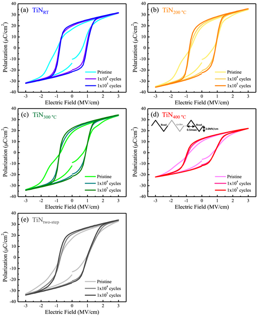
Figure 1. P–E hysteresis loops in the pristine state, after 1 × 10⁴ cycles, and after 1 × 10⁵ cycles: (a) TiNRT, (b) TiN200 °C, (c) TiN300 °C, (d) TiN400 °C, and (e) TiNtwo-step samples. The pulses used for the P–E measurements are shown in (d).
Download figure:
Standard image High-resolution imageFor a more accurate comparison, the polarization values were obtained for each of the 20 samples in the pristine state and at 1 × 10⁵ cycles; these are presented as box plots in figure 2. Because the polarization values were extracted from the P–E hysteresis loops (figure 1), the y-axes of the box plots were marked with a double switching polarization (2Pr s) value. As mentioned previously, the samples capped with TiN TEs grown at relatively low temperatures (TiNRT, TiN200 °C, TiN300 °C) and the TiNtwo-step samples showed almost identical 2Pr s values, which were approximately 30 μC cm−2 and 43 μC cm−2 in the pristine state and at 1 × 10⁵ cycles, respectively. For the TiN400 °C sample, approximately 18 μC cm−2 and 24 μC cm−2 of 2Pr s values were obtained for the pristine state and 1 × 10⁵ cycles, respectively. As a result, the 2Pr s values of the TiN400 °C sample were approximately 40% lower than those of the other samples. In ferroelectric MIM applications, the 2Pr s value determines the memory window [30]. Therefore, it is advantageous to obtain a high 2Pr s value for proper device operation [5].
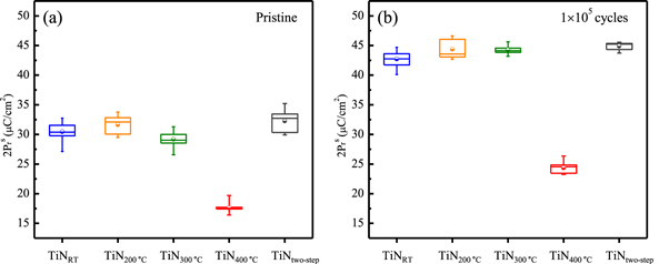
Figure 2. Box plots for 2Pr s value of the TiNRT, TiN200 °C, TiN300 °C, TiN400 °C, and TiNtwo-step samples in (a) the pristine state and (b) 1 × 10⁵ cycles.
Download figure:
Standard image High-resolution imageThe results of the endurance measurements are shown in figure 3. Because the non-switching source (i.e., leakage current) was excluded using the PUND method [31, 32] in the endurance measurements, the y-axis in figure 3 was expressed as the double remnant polarization (2Pr
r) value. All samples showed comparable endurance cycles. Interestingly, the TiNRT, TiN200 °C, TiN300 °C, and TiNtwo-step samples continued to increase their 2Pr
r value above 1 × 10⁷ cycles, whereas the TiN400 °C sample increased its 2Pr
r value by 1 × 10⁵ cycles. As a result, the wake-up effect was much smaller in the TiN400 °C sample. The wake-up effect is one of the most important phenomena involved in the performances of ferroelectric devices; specifically, it increases the Pr valve and coercive field after several electric field cycles [33]. Until now, studies on the wake-up effect have been actively conducted to improve the reliability of ferroelectric devices. [18, 33, 34]. Pešic et al reported two main mechanisms of the wake-up effect in HfO2-based thin films [34]: first, the transition from the non-ferroelectric phases to the ferroelectric o-phase under electric field cycles, and second, the redistribution of defects (mainly oxygen vacancies). A large number of oxygen vacancies in the pristine state can cause a wake-up effect because oxygen vacancies inhibit ferroelectric domain switching [33]. In particular, oxygen vacancies easily accumulate in the interfacial region between the TiN electrodes and the HZO film during fabrication [33]. The wake-up effect occurs when oxygen vacancies are redistributed from the interface region to the bulk region [34]. Considering the high thermal budget of the TiN400 °C and TiNtwo-step samples, it is reasonable to assume that the TiN400 °C and TiNtwo-step samples have more oxygen vacancies than the others. Therefore, we suspect that the reduced wake-up effect in the TiN400 °C sample is attributed to the difference in the phase transition rather than oxygen vacancies. Figure 3. 2Pr
r values as a function of cycle number. The 2Pr
r values were obtained by the PUND measurements. The inset image indicates the pulses used for the PUND measurements. Download figure:

The difference in the phase formation was analyzed in detail to determine the reason for the significantly decreased polarization value. Figure 4(a)–(e) show the GIXRD diffraction patterns of the TiNRT, TiN200 °C, TiN300 °C, TiN400 °C, and TiNtwo-step samples. GIXRD measurements were conducted at a scan rate of 0.006°/s. As reported in a previous study, the peak positions of the monoclinic (−111, P21/c, m-phase), o (111), t (011), and m (111) are located at 28.54°, 30.4°, 30.8°, and 31.64°, respectively [14]. Gaussian curve fitting was performed to compare phase formation [23, 35]. The presence of m-phases was clearly confirmed in the TiN400 °C sample (figure 4(d)), but not in the TiNRT, TiN200 °C, TiN300 °C, and TiNtwo-step samples. The sum of the relative ratios of both m (−111) and m (111) is approximately 43% in the TiN400 °C sample, which was calculated from the integrated area of each peak [35]. The result reasonably explains the cause of the decreased polarization values in the TiN400 °C sample. As the relative ratio of the m-phase increases, the relative ratio of the ferroelectric o-phase is expected to decrease. M  ller et al proved the capping layer effect using a 4-nm-thick TiN TE in a TiN/Y:HfO2/TiN structure [36]. In the TiNtwo-step sample, the 5-nm-thick TiN film grown at RT effectively suppressed the m-phase formation during heating and crystallization of the HZO film, preventing degradation of the polarization value [21]. We observed similar ferroelectric characteristics to the RT/400 °C TiNtwo-step sample from the 200 °C/400 °C and 300 °C/400 °C TiNtwo-step samples (data not shown).

Figure 4. GIXRD diffraction patterns of the (a) TiNRT, (b) TiN200 °C, (c) TiN300 °C, (d) TiN400 °C, and (e) TiNtwo-step samples. (f) Peak positions near 30.5° for the TiN/HZO/TiN capacitors. (g) GIXRD diffraction patterns of TiN/HZO/TiN capacitors with and without subsequent RTA. The diffraction peak positions of the o (200), TiN (111), and TiN (200) planes are marked in (f), and 'w/o' means without. .
Download figure:
Standard image High-resolution imageFrom the perspective of the reliability of device operation, a suppressed wake-up effect is desirable [37]. Therefore, it is necessary to study the cause of the suppressed wake-up effect of the TiN400 °C sample. Figure 4(f) shows the peak positions near 30.5° for the TiN/HZO/TiN capacitors. The GIXRD diffraction peak near 30.5° consists of the t (011) and o (111) characteristic peaks, but classification is difficult owing to structural similarity [14]. The peak positions were calculated using Gaussian fitting in the 2θ range of 27°–33°. For the TiNRT, TiN200 °C, TiN300 °C, and TiNtwo-step samples, the peak positions were observed above 30.55°, whereas the peak position for the TiN400 °C sample was 30.49°. This means that the relative ratio of the o-phase among the t-/o-phases is higher in the TiN400 °C sample than in the other samples. It should be noted that because the TiN400 °C sample has a high amount of the m-phase (∼43%), the absolute amount of the o-phase might be higher in the TiNRT, TiN200 °C, TiN300 °C, and TiNtwo-step samples. This supposition is reasonable considering the high polarization values of the TiNRT, TiN200 °C, TiN300 °C, and TiNtwo-step samples. In any case, the amount of the t-phase was estimated to be lowest in the TiN400 °C sample. Lomenzo et al reported that the phase transition from the t- to o-phase could cause a wake-up effect [38]. In another previous report, the relative free energies of the o-, t-, and m- phases were calculated for a 9-nm-thick HZO film at RT [39]. The most stable phase was the o-phase, with an energy difference of 1 meV/f.u. between the o- and t-phases, and 28 meV/f.u. between the o- and m-phases [39]. The relative energy difference between the o- and t-phases was much smaller than that between the o- and m-phases. Using an experimental method, Park et al demonstrated that the wake-up effect increases when the relative free energy difference between the o- and t-phases becomes small [37]. Therefore, the reduced wake-up effect in the TiN400 °C sample can be explained by the decrease in the t-phase. In contrast, the m- to o-phase transition during electric field cycling would have occurred insignificantly because of the relatively high free energy difference.
Recently, Athle et al reported that the ferroelectric properties of HZO films could be dependent on the TiN TE texture [40]. Their 111-textured TiN TE sample exhibited a high polarization value. They explained that 111-textured TiN can induce high in-plane tensile stress during RTA. In our experiment, it was necessary to confirm whether the difference in the ferroelectric properties was related to the grain orientation of the TiN TEs. Figure 4(g) shows the GIXRD diffraction peaks of the TiN/HZO/TiN capacitors in the 2θ range of 34°–44°.
Samples without the subsequent RTA process were described as 'w/o RTA.' TiN400 °C w/o RTA and TiNtwo-step w/o RTA are not presented in figure 4(g) because neither the TiN400 °C sample nor the TiNtwo-step sample were subjected to subsequent RTA. For the TiNRT w/o RTA and TiN300 °C w/o RTA samples, the diffraction peaks of the o (200) plane of the HZO film are not shown because the HZO films were not crystallized. Furthermore, although their intensities were weak, TiN (111) and TiN (200) diffraction peaks were observed. After the RTA process, the TiNRT and TiN300 °C samples clearly showed not only the TiN (111) and TiN (200) diffraction peaks, but also the o (200) diffraction peaks. Considering that the ALD TiN BEs were deposited at 500 °C, it is reasonable to assume that the ALD TiN BEs were already crystallized before the RTA process. Therefore, we believe that the XRD results mainly indicate the crystallinities of the TiN TEs rather than those of the TiN BEs. The diffraction peaks of the samples are not significantly different. The TiN400 °C and TiNtwo-step samples also showed TiN (111) and TiN (200) diffraction peaks similar to those of the other samples, even though no additional RTA process was performed. These results therefore indicate that the TiN TE texture did not play a major role in determining the ferroelectric properties. However, in the case of ALD TiN deposition, the texture change can be large depending on the process conditions employed [26]. It is therefore necessary to further study the ferroelectric properties of the HZO thin film according to the TiN texture.
Figure 5 shows AFM images of the as-deposited TiN thin films. The TiN thin films were deposited on a Si (0.5 mm)/SiO2 (100 nm) substrate to minimize the effects of the HZO sublayer on the deposition temperature. These images were recorded prior to carrying out the RTA process. The root-mean-square roughness (Rq) values were determined to be 0.232, 0.189, 0.192, and 0.184 nm for the TiN thin films grown at RT, 200 °C, 300 °C, and 400 °C, respectively. The AFM measurements were performed twice for each sample, and we used the smallest Rq values as possible (table 1). The difference in the states of the films grown at 200 °C and 300 °C is minimal. Although the Rq value of the TiN thin film grown at RT was high, the topographies of the TiN thin films were generally uniform. It is well known that roughness is related to the film grain size [41, 42]. However, considering the similar ferroelectric properties of the TiNRT, TiN200 °C, and TiN300 °C samples, the effect of the difference in Rq can be considered negligible. We also calculated the grain sizes of the TiN TEs using the full-width at half maximum and peak positions obtained by XRD measurements (figure 4(g)). The average grain sizes for the TiNRT w/o RTA, TiN300 °C w/o RTA, TiN400 °C, and TiNtwo-step samples were therefore determined to be approximately 8.97, 8.76, 8.65, and 9.91 nm, respectively. The average grain sizes of the TiN TEs for the TiNRT and TiN300 °C samples increased from 8.97 to 9.87 nm and from 8.76 to 9.76 nm, respectively. In other words, the average grain sizes of the TiN TEs increased after the subsequent RTA process. Since the HZO film of the TiN400 °C sample has the smallest grain size of the various samples, it was assumed that this was related to the small grain size of the HZO film (∼ 7.94 nm). It was therefore assumed that the continuous growth of the t/o-phases was hindered due to the presence of the m-phase in the TiN400 °C sample.
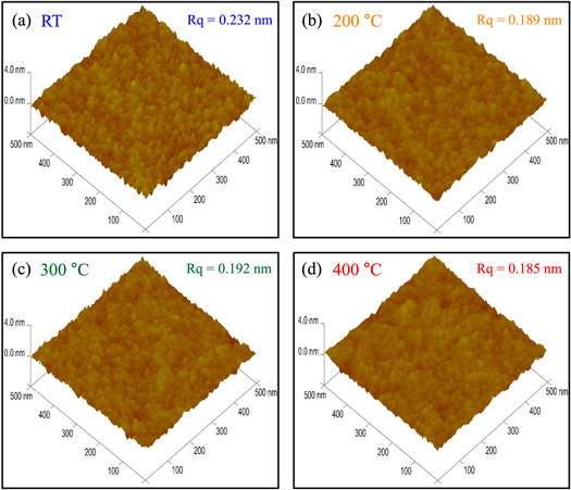
Figure 5. AFM images of as-deposited (a) RT, (b) 200 °C, (c) 300 °C, and (d) 400 °C TiN thin films. The TiN thin films were deposited on a Si (0.5 mm)/SiO2 (100 nm) substrate. 'Rq' indicates the root-mean-square roughness.
Download figure:
Standard image High-resolution imageTable 1. Summary of the Rq values. The Rq values were obtained using AFM measurements.
| TiN film | RT | 200 °C | 300 °C | 400 °C |
|---|---|---|---|---|
| Rq value (nm) | 0.232, 0.279 | 0.189, 0.218 | 0.192, 0.206 | 0.184, 0.185 |
TOF-SIMS analysis was performed to investigate the changes in the film composition and interfacial state by the deposition temperature of TiN. Figure 6(a) and (b) show the results of the TOF-SIMS depth profile for the TiNRT and TiN400 °C samples. Cesium (Cs+, 1 keV) was used as a sputtering source over a 200 × 200 μm2 area, and bismuth (Bi1 +, 30 keV) was used as an ion source over a 50 × 50 μm2 area. TOF-SIMS measurements were performed in the negative mode. In figure 6, ZrO- and HfO- represent the Zr and Hf compositions, respectively. Almost the same film composition was found in the TiNRT and TiN400 °C samples. It is challenging to distinguish the exact interface regions between the TiN electrodes and the HZO film. For the TiNRT sample, the top and bottom interface thicknesses were roughly determined to be 4.9 and 3.8 nm, respectively, while these values for the TiN400 °C sample were approximately 4.5 and 4.1 nm, respectively. Interestingly, similar bottom interfacial regions were observed for each sample despite the fact that the TiN400 °C sample had a high thermal budget. In our previous study [43], we confirmed that TiN BE was mainly oxidized during the ALD process for HZO film deposition. Therefore, it is difficult to say that the decreased polarization value of the TiN400 °C sample is due to the increased thickness of the interfacial region (dead layer).

Figure 6. TOF-SIMS depth profiles for the (a) TiNRT and (b) TiN400 °C samples.
Download figure:
Standard image High-resolution imageTo date, many studies have revealed that parameters such as chemical doping [10, 11], mechanical stress [12, 13], heat treatments [14, 15], and HZO film thickness [14, 44] affect the phase formation of HfO2-based thin films. Here, we focus on how the phase formation of an HZO film is influenced by the deposition temperature of the TiN TE and the fabrication methods. Figure 7 shows a schematic of the phase formation during the RTA and TiN TE processes. During relatively low-temperature TiN processes (below the crystallization temperature of the HZO film, RT–300 °C), the HZO films remained either amorphous or weakly crystallized. In the heating and crystallization steps of the subsequent RTA process, a phase transformation to the t-phase occurs dominantly. At this stage, the phase transformation is determined by a kinetic energy barrier [44, 45]. In the cooling step of the RTA, a part of the t-phase is transformed into the o-phase by an in-plane tensile stress caused by the capping TiN TE [13, 46]. It is generally accepted that capping electrodes also prevent twin deformation, resulting in the suppression of m-phase formation [15, 21]. However, it is not clear whether the in-plane tensile stress significantly influences the o-phase formation during cooling or whether the suppression of the m-phase mainly influences the o-phase formation during heating and crystallization. In the case of the high-temperature TiN process (above the crystallization temperature of the HZO film, 400 °C), the HZO film is almost crystallized during TiN deposition (in situ crystallization) [27, 29]. Even when the heater temperature reached 400 °C and crystallization of the HZO film started, the growth of TiN TE started. Thus, for the 400 °C TiN process, it is difficult to effectively suppress m-phase formation because there is no capping effect during the HZO crystallization process. Park et al reported that the phase transformation to the m-phase is irreversible during RTA [47, 48]. Therefore, the formed m-phase could not transform into the o-phase during the cooling step of the RTA. In the case of the two-step deposition method, the 5-nm-thick TiN film grown at RT suppressed the m-phase formation during heating and crystallization, and the HZO film fully crystallized during the growth of 400 °C TiN (5 nm). Therefore, when the in situ crystallization method is used for the fabrication of ferroelectric TiN/HZO/TiN capacitors, the two-step deposition method using relatively low-temperature TiN (first layer) and relatively high-temperature TiN (second layer) might be useful.

Figure 7. Schematic of the phase formation during the RTA process and deposition processes of the TiN TE.
Download figure:
Standard image High-resolution image
4. Conclusion
In this study, we thoroughly investigated the impact of the deposition temperature of the TiN TE on the structural features and ferroelectric properties of 10-nm-thick HZO thin films, which have a relatively low crystallization temperature (350°C–400°C). Although the TiN400 °C sample showed ferroelectric characteristics without subsequent RTA (in situ crystallization), the polarization value decreased by more than 40% compared with the samples capped with TiN TE grown at low temperatures (TiNRT, TiN200 °C, TiN300 °C samples). The degradation in the polarization value of the TiN400 °C sample is attributed to the increased m-phase formation, which was confirmed by XRD analysis. Through the two-step deposition method, strong ferroelectric properties were achieved using the in situ crystallization method. The two-step deposition method is a promising approach for preventing degradation of the ferroelectric properties of the in situ crystallized HZO thin films.
Acknowledgments
This work was supported by the National Research Foundation of Korea (NRF) under Grant No. 2018R1A3B1052693.
Data availability statement
All data that support the findings of this study are included within the article (and any supplementary files).