
Abstract
The application of solid-state quantum emitters in real-world quantum information technologies requires precise nanofabrication platforms with high process yield. Self-assembled semiconductor quantum dots with excellent emission properties have proven to be among the best candidates to meet the needs of a number of novel quantum photonic devices. However, their spatial and spectral positions vary statistically on a scale that is far too large for their system integration via fixed lithography and inflexible processing schemes. We solve this severe problem by introducing a flexible and deterministic manufacturing scheme based on precise and convenient cathodoluminescence spectroscopy followed by high-resolution electron-beam lithography. The basics and application examples of this advanced in situ electron-beam lithography are described in this article. Although we focus here on quantum dots as photon emitters, this nanotechnology concept is very well suited for the fabrication of a variety of quantum nanophotonic devices based on quantum emitters that exhibit suitably strong cathodoluminescence signals.
Export citation and abstract BibTeX RIS

Original content from this work may be used under the terms of the Creative Commons Attribution 4.0 licence. Any further distribution of this work must maintain attribution to the author(s) and the title of the work, journal citation and DOI.
1. Introduction
Cathodoluminescence (CL) spectroscopy has a long standing tradition as powerful spectroscopy approach with high spatial resolution and high excitation energy [1]. In the field of semiconductors, the CL concept was found to be very suitable for the spatially resolved investigation of low-dimensional heterostructures such as quantum wells and quantum wires [2, 3]. With the advent of quasi zero-dimensional (0D) nanostructures such as self-assembled quantum dots (QDs), CL again demonstrated its capabilities for their detailed optical characterization [4–12]. Due to their small size on the order of the de Broglie wavelength such QDs and other 0D emitters feature discrete energy levels and act as true single-photon emitters (see [13] and references therein). In fact, they became highly prominent for the application as single-photon sources in upcoming quantum information processing (QIP) schemes like photonic quantum computing [14] and quantum cryptography [15].
Despite their excellent optical and quantum optical properties, self-assembled QDs cannot be integrated directly into nanophotonic devices with high control and process yield when using conventional nanotechnology methods such as electron-beam lithography (EBL). In fact, high-quality epitaxial QDs as obtained from the Stranski-Krastanov growth mode [16] show a random spatial distribution and a strong dot-to-dot variation of the emission energy (cf figure 1). This randomness represents a severe obstacle, since the integration of such emitters into nanophotonic structures must be carried out with a spatial accuracy of a few 10 nm at maximum in order to achieve optimal performance in terms of, e.g., photon-extraction efficiency when it comes to single-photon sources which ideally also exhibit broadband efficiency [17–27]. Moreover, in device concepts relying on pronounced cavity-enhanced light–matter interaction also spectral resonance between the emitter and the cavity mode needs to be ensured [28–31]. In addition, advanced applications in photonic quantum technology, such as quantum repeaters, which are based on entanglement distribution via Bell state measurements, require the fabrication of many quantum light sources with identical emission energy and high photon indistinguishably which places very high demands on the manufacturing technology [32–34]. These stringent requirements in the field of quantum nanophotonics stimulated the development of deterministic fabrication techniques where pre-selected quantum emitters are integrated with high accuracy in the photonic structures.

Figure 1. The random distribution of positions and emission energies of self-organized QDs hinders the application of conventional lithography schemes. The simultaneous detection of many QDs results in an inhomogeneously broadened ensemble photoluminescence curve (black) whereas a single QD shows discrete emission lines (red, inset). The lower inset shows an atomic-force microscopy image of a single layer of shallow capped InGaAs/GaAs QDs, demonstrating the random spatial distribution.
Download figure:
Standard image High-resolution image2. Deterministic fabrication techniques for solid state devices
The related deterministic fabrication techniques can be divided into two sub-categories. In the first category, the positions of suitable quantum emitters are determined relative to marker structures on the sample surface by optical mapping. Afterwards, marker-based electron-beam lithography (EBL) [35–37, 21] or direct laser writing [38] are used to define the desired nanophotonic structures aligned to the pre-selected quantum emitters. Other approaches of this type utilize topographic features in atomic force microscopy (AFM) [39] or scanning electron microscopy (SEM) [40] micrographs to pin the emitters' positions before device integration. Despite their success, these techniques have to ensure a very precise matching of coordinate systems in different setups and they suffer from surface blocking by the markers and a non-seamless process flow.
Deterministic in situ lithography techniques on the other hand perform spectroscopy and subsequent lithography in one and the same setup and at the same temperature (e.g. 10 K). The in situ lithography approach was first reported in [41], by combining optical spectroscopy and laser lithography in a confocal micro-photoluminescence setup. This approach is in general very powerful but suffers from the limited capabilities of optical lithography in terms of resolution and design flexibility. In contrast, in situ lithography based on the combination of cathodoluminescence spectroscopy and EBL, namely in situ EBL, can benefit from the full potential of high-resolution EBL. First steps into this direction were presented in [42], where in situ EBL was used to make electrical contacts to nanowires. The further development and application of in situ EBL in (quantum) nanophotonics was reported in [43], in which pre-selected QDs were integrated deterministically into sub-μm mesa structures.
3. In situ EBL - Method and Experimental
Based on first results, we optimized the in situ EBL approach by setting up the hardware and developing the required software environment and processing technologies. A crucial point in the development process was selecting suitable EBL resists and investigating and pioneering their application in low-temperature EBL as described below.
In situ EBL requires the consecutive and seamless combination of CL spectroscopy and EBL in one and the same setup to benefit from the full potential of this deterministic device technology. A suitable system consists of a SEM or EBL setup equipped with a CL extension. Depending on the samples under investigation, also a cryostat for low-temperature operation may be required. As we intensively deal with InGaAs/GaAs QDs that require low-operation temperatures to maximize the luminescence yield and minimize the detrimental interaction with phonons, a cryostat for sample temperatures as low as 5 K is prerequisite for in situ EBL of such QDs. It is interesting to note that in case of quantum emitters with higher thermal stability, like nitrogen vacancy (NV) centers in diamond, in situ EBL could also be performed in a simpler mode at room temperature.
Our prototype in situ EBL setup is based on a JEOL JSM 840 SEM and a custom made CL add-on. The high-resolution spectrometer is equipped with a Si-CCD camera and an InGaAs 1D array detector to cover the spectral range from 300 nm to 1700 nm. The system has a spectral resolution (FWHM criterion) better than 65 μeV at 930 nm and the peak positions of emissions lines can be determined with an accuracy of 1 μeV by fitting of the line profiles. Because we are focusing on the processing of In(Ga)As/GaAs QDs, the standard sample stage was replaced with a He-flow cryostat for sample temperatures down to 5 Kelvin. The EBL functionality is realized via a high-voltage beam blanker ( ≈ 50 ns time response) and a homemade pattern generator that utilizes a fast and programmable AD/DA converter card. For time resolved CL spectroscopy a fast (< 50 ps time response) beam blanker can be inserted right below the gun section. This also enables Hanbury Brown and Twiss (HBT) type measurements [44] as shown below. The operating software provides a seamless and time-efficient work flow of CL and EBL operation and is written in LabView. A schematic of our setup is displayed in figure 2 which includes all key components.
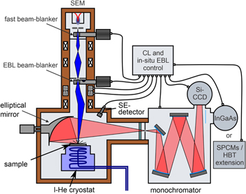
Figure 2. Sketch of our custom made in situ EBL setup. The base unit is a scanning electron microscope of type Jeol JSM 840 that is equipped with a He-flow cryostat, a CL extension, and two beam blankers for EBL and time-resolved measurements, respectively. A Si-CCD camera and a 1D InGaAs diode array (both cooled with liquid nitrogen) cover the spectral range from 300 nm to 1700 nm. The exit ports of the monochromator can also be connected to single-photon counting modules (SPCMs) in a stand-alone or HBT configuration for time-resolved (correlation) measurements. The software and hardware of the CL and in situ EBL controls are fully interlinked. Adapted with permission from [45].
Download figure:
Standard image High-resolution imageA special difficulty and challenge of in situ EBL relates to the EBL resist. In fact, the in situ EBL process starts with spin-coating the sample with e-beam resist. Thus, the sample is already coated with the resist in the initial CL mapping step used for pre-selecting suitable quantum emitters. Importantly, this process step introduces a non-avoidable electron dose to the resist (cf figures 3 and 4). Typical CL mapping doses are in the range of 1 − 7 mC/cm2 which exceeds the clearing dose of all typical positive-tone EBL resists. Consequently, patterning of the resist in the positive-tone regime is no option for the in situ EBL process. The same holds for standard negative-tone resists. Our solution was to identify and utilize EBL resists that undergo a positive- and a negative-tone regime for increasing electron dose. Such resists comprise PMMA and CSAR62. Temperature-dependent investigations of these resists revealed that their respective onset doses are shifted to larger values by more than 5 mC/cm2 when cooling down to low temperatures [46, 47]. This is very beneficial as it enables longer dwell times for the CL mapping without entering the negative-tone regime. Figure 3 shows the afore mentioned characteristics by means of contrast curves of PMMA and CSAR62 for low temperature. Despite the low-temperature and negative-tone operation of the EBL resists, lateral features of acceptable small size are still feasible. With PMMA we were able to demonstrate continuous ridge structures with a width of only 65 nm [48]. When using CSAR62 even features below 50 nm could be obtained [47]. Our initial low-temperature application of PMMA led to a number of written resist patterns that were peeled off when returning to room temperature. This detrimental effect could be related to frozen cracking products that expand upon warming up and rip of the inverted resist above. Application of a wide-area pre-exposure dose was found to circumvent this problem [49]. In case of CSAR62 this resist peeling is absent why CSAR62 became our standard resist for in situ EBL.

Figure 3. Contrast curves for the resists PMMA 950k and CSAR62 for a sample temperature of 7 K. The CL mapping is performed in a dose range that corresponds to the positive-tone regimes of the resists while the EBL patterning happens in the negative-tone regime. Reused with permission from [50].
Download figure:
Standard image High-resolution imageWhilst using such resists, the CL mapping is performed in an electron dose range that corresponds to the positive-tone regime (left area in figure 3) and the actual patterning is done by applying additional electron dose and utilizing the negative-tone regime (right area in figure 3), where the inverted resist acts as etch mask in the subsequent etching step (cf figure 4). Besides the unavoidable requirement to use this dual-tone scenario, the negative-tone regime also exhibits a smaller slope of the contrast curve than the positive-tone regime (cf figure 3) which is very beneficial for 3D greyscale lithography: In this lithography mode, the resist thickness after development directly determines the local etching depth and by thus the 3D profile. Consequently, a smaller slope results in a smaller deviation of the envisaged etch depth when the corresponding electron dose is not exactly met. This is of great importance when structuring, e.g., microlenses using 3D greyscale lithography [49].

Figure 4. Scheme of the in situ EBL work flow. The (epitaxial) sample is spin-coated with resist in a clean room and mounted onto the cold finger of the cryostat in the in situ EBL setup. After CL mapping, suitable luminescence sites are selected in the CL map and the resist is patterned in its negative-tone regime at the extracted positions. Further processing is done in a clean room, again. This includes development of the resist and pattern transfer into the sample by e.g. dry etching. Parts are adapted with permission from [20] and [48].
Download figure:
Standard image High-resolution imageThe general process flow of in situ EBL is sketched in figure 4. Resist-coating of QD-heterostructure templates is performed in a cleanroom with typical resist thicknesses in the range of 80 to 300 nm. The chosen resist thickness depends on the envisaged etch depth and is calculated from the ratio of etch resistances of resist and semiconductor which is about 5 in case of GaAs. The resist-coated sample is attached to the cold finger of the cryostat of the in situ EBL setup and cooled down to 5–10 K. Then a CL map is recorded. The dimensions of the map depend on the sample and planned structuring and are typically in the range of 20 μm x 20 μm to 50 μm x 50 μm. The resulting map is searched for localized emission of quantum emitters, like QDs, whose exact positions are determined by a 2D Gaussian fitting algorithm with 10-20 nm accuracy. Thanks to the highly resolved spectra, not only the position but also the emission wavelength of the emitter is a parameter of the selection process which is set by choosing the corresponding wavelength range for displaying the CL map. This feature is very important for quantum devices and applications requiring a spectral matching of the selected quantum emitters with, e.g., the cavity mode of a QD microcavity device. If additional fine-tuning is required, spectral tuning via temperature, electric field or external strain can be applied (see below). Next, EBL patterns are written at the chosen position(s). The overall workflow (including mapping and EBL at different positions - cf figure 5) is very fast (< 5 min) and can be performed several times consecutively on the sample. When finished, the sample is warmed up and further processing like resist development and (dry) etching is done in a cleanroom. Typically, the negative-tone resist patterns are directly used as etching masks as the etch-rate ratio of semiconductor to resist is sufficiently high (e.g. 5:1 for GaAs vs CSAR62 [47]). It should be noted that there are no detrimental charging effects during the low-temperature in situ EBL process when using the above-mentioned resists. In fact, there are no indications that the cold resist is building up charge that would lead to a Stark shift of emission lines or to a distraction of the electron beam while performing the CL mapping or the EBL writing step.

Figure 5. Fast and parallel processing of many nanostructures is possible by selecting a number of QDs in a single CL map. The rendered sketches include real CL maps as taken during the in situ EBL process and after etching of the mesa structures.
Download figure:
Standard image High-resolution imageAn important figure of merit of the in situ EBL process is the overall alignment accuracy which includes the determination of an emitter's position and the alignment of the nanophotonic structure to this emitter. This number was evaluated by extracting the position of a single QD more than a thousand times and by writing cross hairs on luminescent spots in a shadow mask. The convoluted standard deviations of both investigations yield a value of 34 nm [48] which we treat as our accuracy for the full in situ EBL process. The limited accuracy is mostly related to the brightness of the emitters and the thermal stability of the cryostat, as detailed here: Brighter emitters result in a better signal-to-noise ratio of the CL map and the 2D fitting results are more precise. Alternatively, smaller dwell times in combination with a smaller voxel size for the CL map can be chosen without reaching the onset dose of the resist. The resulting finer grid of the CL map increases the fitting accuracy, too. At the same time, the cold finger of the bulky cryostat is subjected to a slow thermal drift that stabilizes to a speed of several nm per minute after 1–2 hours. This can be improved by choosing a more centric design of the cryostat and a symmetric fixation with thermal isolation to the mounting plate.
As stated before, we have the choice of 2D "black and white" or 3D "greyscale" lithography and patterning. The 2D mode is easily realized by choosing an electron dose in the negative-tone regime where the contrast curve flattens. For the latter one, the local electron dose is varied in correspondence to the greyscale curve of the resist (cf figure 3) to end up with a tailored 3D resist pattern after development [49]. This pattern is directly transferred into the semiconductor by dry etching. The etch ratio of resist and semiconductor introduces a stretching factor that is taken into account when choosing the initial resist thickness beforehand with respect to the required etching depth.
For delicate structuring the omnipresent proximity effect has to be taken into account: First, the point spread function [51] is measured for the respective resist thickness and sample structure. A home-made iterative proximity correction algorithm is then applied with input parameters from the point spread function [52]. The resulting and corrected dose pattern is finally written in the greyscale lithography mode to obtain the envisaged dimensions of 2D or 3D structures.
Another important point of concern is whether the written structures reside completely inside the mapping field or if they extend over the mapping field like prolonged waveguide structures in the field of integrated quantum photonic circuits. In the latter case a neat dose matching for the waveguide parts inside and outside the mapping field has to be ensured to account for the additional mapping dose [53]. Otherwise the waveguide would be of decreased width outside the mapping field and there will be optical losses at the imperfect joint section.
We would like to note that in situ EBL can also be combined with a marker-aided approach [44]. This is necessary in case of extensive pre-characterization that would introduce an electron dose beyond the onset dose of the resist's negative-tone regime. Examples are polarization-, power-, and time-resolved measurements. Another scenario comprises pre-characterization in, e.g., a micro-photoluminescence (μPL) setup. When the pre-characterization is finished, the sample is coated with resist and in situ EBL is performed. Contrary to the marker-based approaches described in the last section, the markers are used for a coarse relocalization of the selected emitters, only. The precise localization happens again via the CL map of the standard in situ EBL process. It is planned to utilize this approach for a detailed statistical analysis of the impact of deterministic device integration on the quantum optical properties of quantum emitters in terms of single-photon emission and emission of indistinguishable photons.
4. Fabricated devices and experimental results
This section details a number of results and quantum devices that were obtained by applying deterministic in situ EBL to semiconductor QD samples. Thanks to the high resolution capabilities of this processing platform and the discrete energy structure of QDs, this combination is highly suited to fabricate devices for applications in single-photon (on-chip) photonics. Important building blocks in this field are efficient (stand-alone) single-photon emitters and on-chip waveguides and linear optical elements.
4.1. Single-photon sources featuring enhanced light extraction
Single-photon sources (SPSs) constitute the 'starting point' for quantum photonic applications that build upon the usage of single photons as information carriers or qubits. The performance of the SPS limits the overall efficiency of the whole schemes. Consequently, SPSs with high photon fluxes and reliable on-demand emission are required for the envisaged applications. The underlying principles are the intrinsic generation of single photons at a high rate and the efficient transmission into connected optical elements.
Self-assembled semiconductor QDs with spontaneous emission lifetimes of about 1 ns provide emission rates up to 1 GHz that can be further enhanced in microcavity structures via the Purcell effect [54]. On the other hand, the high refractive index contrast between semiconductor and air hampers the outcoupling of photons due to total internal reflection [55]. This results in outcoupling efficiencies as small as 1–2% for QDs below planar surfaces (cf left side of figure 6). A neat way to circumvent this detrimental back reflection is to structure the sample surface and to integrate mirror structures below the QDs (cf right side of figure 6). The most intuitive structure to prevent total internal reflection at the top interface by a curved surface is a lens. It also allows for a tailored far field by optimizing its shape via numerical (finite elements method) calculations [24]. For example, an efficient coupling into single-mode fibers is of great interest for distant quantum devices. Another appealing feature of such lenses is their broadband efficiency which means that the increase in efficiency is true in a spectral window of, e.g., 10 nm. This broad-band feature allows for the efficient utilization of, e.g., exciton and biexciton emission for the generation of polarization-entangled photon pairs [56]. Figure 7(a), (b) display such lenses of different geometry. Another structure that promises a very high extraction-efficiency of more than 95% together with a broadband enhancement is the bullseye structure [21, 27, 57]. It comes along with a noticeable Purcell factor of up to 30 and is very well suited for the coupling to single-mode fibers, too [58].
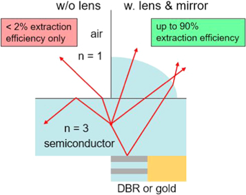
Figure 6. Application of lens structures and bottom mirrors (distributed Bragg reflectors (DBR) or a gold layer) for enhanced light extraction.
Download figure:
Standard image High-resolution image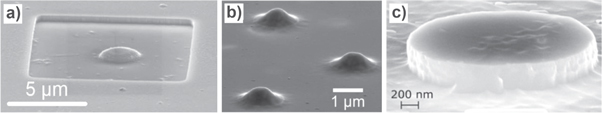
Figure 7. Collection of in situ EBL fabricated structures for enhanced light extraction. (a) and (b) demonstrate hemispherical and Gaussian-shaped lenses and (c) shows a micromesa. Reused with permission from [20, 59], and [60].
Download figure:
Standard image High-resolution imageBesides the more complex structures mentioned above, simple micromesa structures are very efficient, too (figure 7). This is mainly related to weak cavity effects and the related guiding of light via vertical photonic modes inside the structures. Especially when it comes to the coupling into external (single-mode) fibers, mesa structures were identified to promise very high coupling efficiencies via numerical calculations [24] and they provide for a broadband enhancement, too.
Overall, in situ EBL was used to realize a number of such structures for enhanced light extraction. An exemplarily compilation of such structures is shown in figure 7.
First lens and mesa based quantum light sources were fabricated based on InGaAs/GaAs QD samples with a bottom DBR section for operation in the 930 nm wavelength range [20, 43]. Such QDs are very mature at the time being and excellent quantum optical results could be achieved from such SPSs, like almost ideal and excitation-power independent single-photon emission (g(2)(0) < 0.01) [20], highly indistinguishable photons (V = 96%) [61], entangled photon pair emission (F = 0.8) [56], and indistinguishable photons from remote sources could be demonstrated, too [62]. Respective spectroscopic results are given in figure 8.

Figure 8. Optical characterization of QD-microlenses that were fabricated via in situ EBL. (a) Photon autocorrelation traces for different excitation densities, all with g(2)(0) <0.01 that clearly demonstrate emission of single photons. Adapted with permission from [50]. (b) Hong-Ou-Mandel measurement for 2 ns spaced excitation pulses resulting in V = 94% (blue (grey): co- (cross-) polarized, red: fit to the data). Reused with permission from [61]. (c) Quantum tomography for two QD-microlens structures (QDM1 and QDM2) demonstrating biexciton-exciton entanglement with F as good as 0.8. Reused with permission from [56].
Download figure:
Standard image High-resolution imageThe time-resolved CL mode by using the fast beam blanker allows for similar measurement in our in situ EBL setup, too. The largest obstacle is given by the temperature drift of the cryostat which is much larger than in an optimized μPL cryostat. However, time resolved CL measurements on single QDs [11] and even autocorrelation measurements in a HBT configuration [44] are feasible as shown in figure 9.

Figure 9. Time-resolved CL examples for QD-micromesas that were fabricated via in situ EBL. (a) Luminescence traces for one and the same QD before and after processing of the mesa. A slight Purcell enhancement speeds up the emission process in case of the mesa structure. (b) Autocorrelation measurement with a deconvoluted g(2)(0) value of 0.24. Reused with permission from [44].
Download figure:
Standard image High-resolution imageThe next generation of SPSs included structures with a bottom gold mirror [60] and structures that were attached to piezo actuators by a flip-chip process and thermo-compression gold bonding [63]. A bottom gold mirror promises higher photon-extraction efficiencies as there is no limited angle-of-acceptance for reflection as in the case of a bottom DBR. Again, very good quantum optical characteristics could be proven and strain-tuning of the emission energy via the piezo actuator allowed for a tuning range of up to 2.5 meV [63].
Another important discipline in quantum photonics is the plug-and-play integration into fiber-based quantum communication networks. For this, fiber coupling is of utmost importance. Lens structures that were fabricated by in situ EBL were successfully coupled to optical (single mode) fibers by an optical alignment process and hard-contact gluing [64] as well as by a newly established plug-and-play concept that utilizes 3D laser-written fiber chucks and micro optics for increased coupling efficiencies [65].
While the afore mentioned wavelength regime around 930 nm is good for on-chip or short distance communication, mid- and long-distance transmission is ideally realized with photons in the 1.3 μm or 1.55 μm range to benefit from low dispersion and low loss features of conventional fibers. Consequently, the in situ EBL setup was extended with a 1D InGaAs array detector to get access to this wavelength regime [66]. Application of such a detector suffers from a much worse signal-to-noise ratio as compared to the utilization of a Si-CCD camera. At the same time, the fabrication of high-quality InGaAs/GaAs QDs with emission at 1.3 μm is much more demanding as it requires strain-relief techniques to shift the emission beyond 1.1 μm [67]. Nevertheless, the in situ EBL was successfully adapted to the telecom wavelength regime and even indistinguishable photons could be demonstrated [68]. Finally, the gold-bonding technique and piezo-tuning could be realized here, too [69]. For direct fiber coupling a novel approach based on laser interference positioning was successfully applied, ending up in a stand-alone plug-and-play SPS with emission at 1.3 μm [70].
4.2. Building blocks for photonic quantum circuits
So far we have concentrated on isolated single-photon emitting structures and devices based on structuring of discrete sample sites above QDs. Another class of upcoming nanophotonic devices comprises on-chip quantum photonic circuits [71]. The idea is to bring the full functionality from SPSs, over photonic quantum circuits to single-photon detectors onto a single (hybrid) chip [72, 73]. Naturally, on-chip waveguide structures, filters, and beam splitters will be used for routing and manipulation of the single photons. In situ EBL with its high-resolution lithography capabilities seems well suited to tackle this challenge when it comes to randomly distributed emitters, like e.g. QDs, as single-photon sources. For this, the software part of our in situ EBL platform was extended to fabricate waveguide structures with deterministically integrated emitters. The workflow is similar to that presented before and is shown in figure 10.
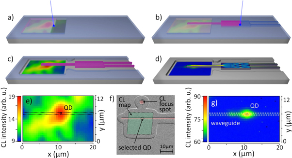
Figure 10. Exemplary scheme for the fabrication of waveguide structures with deterministically integrated QDs and on-chip optical elements. Here, the QD emission is guided into a 1x2 multi-mode interference beam splitter. (a) a CL map is taken to select a single QD, (b) the waveguide system is precisely aligned to the position of the QD during the EBL step, (c) the resist is developed, and (d) the resist profile is transferred into the semiconductor by dry etching. (e) and (g) show CL maps from the in situ EBL CL mapping and the final device, respectively. (f) resembles a false-color SE image of the CL mapping area and the beginning of the waveguide structure. Reused with permission from [53].
Download figure:
Standard image High-resolution imageThe first structure realized is based on InGaAs QDs in a ridge GaAs waveguide above an AlGaAs cladding layer [53]. A 50:50 beam splitter was realized via a multi-mode interference device [74] which offers higher robustness against fabrication deviations as compared to evanescence field couplers [75]. Special care was taken to guarantee the same applied dose for the waveguide part inside and outside the CL mapping field. Micro-photoluminescence investigations confirmed the functionality of the device by means of a true 50:50 splitting ratio as measured on the two output ports and real single-photon emission as this device assembles an on-chip HBT configuration [53]. This device already demonstrates the suitability of in situ EBL for the deterministic fabrication of the most important on-chip components for quantum photonic circuits and networks. Further exploitation of the high spatial selection accuracy of emitters allowed for the realization of directional emission from QDs in waveguides based on chiral effects [52].
Larger quantum photonic circuits that route single photons require lowest-loss circuits. While the InGaAs/GaAs/AlGaAs material system is highly suited for the realization of high-quality SPSs, its waveguiding capability is behind that of Si-based circuits. Si-based systems on the other hand side lack the availability of efficient single-photon emitters. These facts motivate the way for hybrid systems where the best of different worlds is combined [76]. In [77] we report on the deterministic integration of InGaAs QDs in GaAs slabs that are waferbonded onto SiN/SiO layers beforehand (figure 11). First, a thin GaAs membrane with a single sheet of InGaAs QDs was wafer-bonded onto a SiN/SiO/Si template. The resulting hybrid sandwich structure was spin-coated with CSAR62 resist and the in situ EBL process was performed to integrate selected QDs into tapered GaAs slabs. Finally, underlying and elongated SiN/SiO waveguides were fabricated by standard EBL.

Figure 11. Realization of a hybrid GaAs/SiN/SiO waveguide structure with a deterministically integrated InGaAs QD. (a) In situ EBL is performed on an InGaAs/GaAs-QD slab that was bonded onto a SiN/SiO template. (b) The in situ EBL written and tapered GaAs structure is freed from surrounding GaAs. (c) The SiN/SiO waveguide structure is fabricated by standard high-resolution EBL. Sketch (d) and SEM micrograph (e) of the final device. Reused with permission from [77].
Download figure:
Standard image High-resolution image
The resulting structure was demonstrated to preserve the quantum optical quality of the integrated InGaAs/GaAs QD and also showed the emission of indistinguishable photons in HOM measurements with temporal post selection [77].
5. Summary and outlook
The combination of low-temperature CL spectroscopy and low-temperature electron-beam lithography is shown to provide a very precise and powerful nanotechnology tool for the deterministic integration of quasi zero-dimensional light emitters into nanophotonic structures. The high-resolution EBL step not only allows for black and white patterning but also gray-scale lithography is feasible to fabricate 3D profiles. First, lens and mesa structures were introduced that enhance the light extraction from the semiconductor structure while maintaining the exquisite quantum optical properties of the integrated QDs. While a standard DBR as bottom mirror enables an easy device processing, a bottom layer of gold not only increases the possible light extraction further - it also enables bonding onto piezo actuators for strain tuning of the QDs' electronic structure.
The upcoming need for miniaturized and compact all-on-a-chip structures led to the extension of our in situ EBL approach for the fabrication of deterministic waveguide structures. First results were obtained with purely InGaAs/GaAs/AlGaAs based structures before in situ EBL was successfully applied for the realization of hybrid waveguide systems by combining the afore mentioned GaAs-based material with underlying SiN/SiO waveguide systems, too. This best-of-two-worlds combination will enable the fabrication of extended low-loss waveguide circuits with integrated high-quality quantum emitters.
It must be noted that the reported technological developments and results were obtained with an outdated SEM-based system that lacks state-of-the-art components like a laser-interferometer sample stage and an up-to-date electron column for highest spatial EBL resolution and accuracy. Consequently, we have started to transfer our technology and know-how onto a new commercial in situ system with state-of-the-art EBL capabilities to bring in situ EBL to a next level in the near future. Our new in situ EBL system based on a Raith eLine Plus includes a CL mirror between the pole piece of the electron column and the sample for a significantly higher collection efficiency of vertically emitted CL emission. This system has an interferometer stage for precise and stitching-free lithography, allows for continuous waveguide writing, and features an improved cryostat mount to minimize its thermal drift.
Acknowledgments
We acknowledge funding from the German Research Foundation via the projects SFB787, Re2974/12-1 and Re2974/24-1, from the project EMPIR SIQUST (the EMPIR initiative is co-funded by the European Union's Horizon 2020 research and innovation program and the EMPIR Participating States) and from the EU via the International Training Network QUDOT-TECH.
Data availability statement
No new data were created or analysed in this study.