
Abstract
A stack of five Al(Ga)N-based quantum wells is investigated by combined laterally and depth resolved cathodoluminescence (CL) spectroscopy in order to distinguish lateral and vertical inhomogeneities of these wells. Transmission electron microscopy (TEM) micrographs provide data for the real sample structure, which enters into the Monte-Carlo simulation of the depth-resolved CL measurements to refine the depth resolution. The comparison of these CL measurements to the results of electron energy loss spectra (EELS) allows to identify local thickness variations of the lower three quantum wells to be the origin of two different luminescence contributions to the overall spectrum. The differentiation of the two groups of quantum wells by depth-resolved CL is demonstrated.
Export citation and abstract BibTeX RIS

Original content from this work may be used under the terms of the Creative Commons Attribution 4.0 licence. Any further distribution of this work must maintain attribution to the author(s) and the title of the work, journal citation and DOI.
1. Introduction
Scanning electron microscopy cathodoluminescence (SEM-CL) is a non-destructive characterization technique for semiconductors, which provides detailed information about the investigated sample, such as bandgap (composition), defect density, and visualization of single or bundles of structural defects [1, 2]. The spatial resolution is determined by the primary electron beam diameter, the width of the excitation volume inside the semiconductor crystal, and the diffusion length of the primarily excited charge carriers [3]. Depending on the actual material, either the dimensions of the initial excitation volume or the subsequent carrier diffusion limit the resolution [4]. Instead of preparing very thin and comparably small cross sectional samples like the ones needed for transmission electron microscopy investigation, depth resolution can also be obtained in conventional SEM-CL by stepwise variation of the primary electron beam energy in order to control the electron penetration depth [5, 6]. From Monte-Carlo simulations (MCS) of the primary electron scattering inside the crystal, the corresponding maximum depth of the luminescence signal origin can be derived. Using this method, e.g. Brillson et al investigated Ga(In)N-based quantum wells by depth-resolved cathodoluminescence spectroscopy (DRCLS) and found localized states near the quantum well [6].
We present laterally and depth-resolved SEM-CL measurements on an AlN/AlGaN multiple quantum well (MQW) stack comprising five nominally identical quantum wells (QWs). Some of the QWs were found to emit at different emission energies. By the combination of DRCLS, high-resolution transmission electron microscopy (HRTEM), and electron energy loss spectroscopy (EELS), the varying thickness and composition of the QWs could be identified as a reason for the multiple spectral contributions. DRCLS was found to be able to distinguish between two groups of quantum wells. Different from CL carried out in a scanning transmission microscope (STEM-CL), this CL investigation in plan-view geometry is non-destructive, covers a large volume of the sample, does not require any sample preparation, and is therefore independent of artifacts from preparation. The combination with TEM imaging allows a benchmarking of depth-resolved cathodoluminescence.
2. Fundamentals
2.1. Simulation of the excitation volume
The depth resolution used in our study is modeled by a self-written code for MCS of the primary electron (PE) scattering, which is quite similar to the well-known 'CASINO' of Drouin et al [7], but is specifically adapted to take into account also diffusion and local variation of the band gap energy. A detailed description of the simulation process can be found in our earlier publication [8].
The most important steps are briefly sketched in this section, and the simulation model is altered to account for charge carrier capture at the quantum wells. The simulation starts at the sample surface by considering a single PE with defined energy E0. Similar to the well-known CASINO software, the scattering process of the electrons is divided into two parts: An elastic one which is only responsible for the change of the direction and an inelastic one which accounts for the energy loss occurring along the path between two of these elastic scattering events. This 'continuous slowing down approximation' (CSDA) will be discussed later in this article. For the elastic part, the scattering cross section  is calculated. The analytical, semi-empirical approximation of the Mott scattering cross section published by Gauvin and Drouin [9, 10] reads

where λ and β are material constants. E is the actual electron energy in keV, Z is the atomic number, and α denotes a screening factor [11]. β and λ can be calculated using equation (2) and (3) [9, 10]:


Gauvin and Drouin fitted these parameters to tabulated numeric solutions of the scattering's Dirac equation in order to save computing time [9]. The mean free path Λ of the electron in the solid can be derived from the cross section calculated in equation (1) by the expression [12]

where NA is Avogadro's constant and A the mass number. For the density of mass ϱ, a value of 6150 kg/m3 was used for GaN [13] and 3255 kg/m3 for AlN, respectively [14]. The values for ternary AlGaN were calculated by linear interpolation. The final length of the n-th path element sn the electron travels between two scattering events reads [15]:

where R is a random number between 0 and 1. Following the CSDA, the electron is considered to loose its energy continuously along the path between two scattering events. Here, the empiric formula of Zhenyu and Yancai based on the equations of Joy and Luo is applied [16, 17]. The mean ionization potential is taken from Berger and Seltzer [18].
Subsequently, the polar scattering angle Θ (in degrees) can be calculated from the partial elastic Mott cross-section [19]

R is again a random number equally distributed between 0 and 1. α* and β* are material parameters, which are a function of the actual electron energy. The azimuthal scattering angle is assumed to be homogeneously distributed over 2π. The simulation algorithm is repeated, until the residual energy of the PE drops below 50 eV. This scattering simulation is repeated for 15,000-23,000 primary electrons, depending on the corresponding experimental PE current. During this MCS, the energy loss of the PEs is summed up at each position inside the excitation volume. By integration over the x-y-plane (i.e. the plane parallel to the sample surface), a depth profile of the energy deposited is calculated. The number Q of excitons created for each depth reads

where W is the deposited energy [15]. The effective energy  required to create an exciton depends on the band gap energy EG
. Alig and Bloom [20] determined the relation
required to create an exciton depends on the band gap energy EG
. Alig and Bloom [20] determined the relation

Subsequently, the axial diffusion (i.e. parallel to the incident electron beam) is also taken into account by convolving the exciton creation depth profile with a Gaussian, which decays to 1/e over the exciton diffusion length L. To account for the increased capture of the diffusing excitons by the quantum wells, a local effective diffusion length of 1 nm is introduced, which is applied to the simulation results at the assumed position of the quantum wells instead of the bulk diffusion length. Hence, the charge carriers are effectively confined to the quantum wells. The results are also discussed for a larger effective diffusion length of 10 nm in the results section. For unknown structures, the input parameters of the structure might be varied, until simulation and experimental data are consistent with each other.
2.2. Calculation of the quantum well emission energy
To determine the Ga- or Al-content in the quantum wells embedded in an AlN matrix from the emission energy, the eigenstates were calculated from the corresponding Schrödinger equation, which is solved by an approximation following the approach of van der Maelen Uría et al based on a numerical matrix method [21]. The quantum wells are supposed to grow pseudomorphic, i.e. they reproduce the lattice constant of the bulk material and are therefore fully strained. For the lattice constants of AlN, the values published by Paszkowicz et al were used [22]: c = 4.98 Å and a = 3.11 Å. The corresponding parameters of GaN are c = 5.19 Å and a = 3.19 Å, respectively [23]. The unstrained lattice constants of the QWs were interpolated linearly. The elastic constants were taken from [24] and [25], and for the deformation potentials, the values of Ishii et al were used [26, 27]. The band gap energy is calculated with a bowing parameter of 0.9eV [28]. In addition to the discontinuity of the spontaneous polarization [29], the piezoelectric polarization has to be taken into account, because the AlGaN quantum wells are strained by the surrounding bulk AlN. The values of the piezoelectric constants were taken from [29, 30] and were interpolated linearly for the ternary well material.
3. Sample description and preparation
The sample under investigation was grown by metalorganic vapor phase epitaxy. A schematics of the vertical structure is shown in figure 1. First, bulk hexagonal c-oriented AlN was grown on a sapphire substrate (orange in sketch). Subsequently, five nominally identical AlGaN quantum wells were deposited (red). The QWs were grown at 1160 ◦C surface temperature and 80 hPa ambient pressure with tri-methyl gallium (TMGa) and tri-methyl aluminum (TMAl) as precursors, with their flows set to 27 and 18 μmol/min, respectively. The growth time was 45 s for each quantum well, which was expected to result in a thickness of 3 nm. The AlN barriers (orange) were grown at 1145 ◦C and 35 mbar with TMAl precursor with a flow of 22 μmol/min. The growth time of the barriers was 2 min, aiming at a nominal thickness of 7 nm. The cap layer (blue) consists again of binary AlN, and has a nominal thickness of 30 nm. In summary, the quantum wells should be located 30, 40, 50, 60, and 70 nm below the surface.

Figure 1. Schematics of the sample under investigation. The quantum wells are marked in red.
Download figure:
Standard image High-resolution imageFor TEM investigation, two lamellas were sticked face to face and one cross-sectional piece was cut out. The cross-sectional sample was further processed including grinding, dimpling and ion milling. The sample was thinned by grinding to a thickness of ca. 100 μm and subsequently dimpled from both sides to less than 5 μm. A Fischione Ion Mill 1010 was used for ion milling with a milling voltage of 5 kV and an inclination angle of 10°. To reduce ion-bombardment-induced amorphization, the sample stage was cooled by liquid nitrogen during the ion milling process.
4. Experimental
All CL measurements were carried out in a hot field emitter type scanning electron microscope (SEM) Zeiss LEO DSM 982. A liquid helium-cooled cryostat allows sample temperatures between 7 K and 475 K. The SEM is equipped with an UV-enhanced glass fiber, touching the sample under an angle of about 27° relative to the surface, which collects about 15% of the luminescence light emitted by the sample. Larger particles (which were used for drift correction) can therefore cause shadowing of the luminescence. The amplitude of the surface roughness is too low to cause shadowing. The advantages of this method of light collection are a low working distance (less than 5 mm), a fully functional inlens detector system, and the possibility of measurements with very low primary energies down to 400 eV. Spectra are recorded by a nitrogen-cooled open-electrode charge coupled device (CCD) with a quantum efficiency of about 30%, which is attached to a 90 cm focal length monochromator. In the configuration used for the measurements presented here, a 1200 mm−1 grating blazed for 330 nm was used. The spectral resolution was set to 8 meV at 4.8 eV emission energy. Alternatively, a pivoted mirror can redirect the luminescence light to a smaller 25 cm focal length monochromator equipped with a photomultiplier tube in order to record a series of wavelength-selective CL maps. The resolution of the latter monochromator was set to 73 meV at 4.8 eV, using a 1200 mm−1 grating blazed for 250 nm. The CL measurements were carried out at approximately 8 K sample temperature, and the PE energy was varied in 0.5 keV steps between 1 and 10 keV, with a sample current between 110 pA (at 1 keV) and 170 pA (at 10 keV). The resulting non-constant excitation power also enters in the simulation parameters by varying the numbers of simulated electrons proportional to the sample current. The spectra for the depth-resolved measurement were recorded on a 35 × 30 μm2 area, containing a small particle on the sample surface, which was used for spatial correlation and compensation of charge-related drift. This particle was checked not to contribute to the luminescence spectrum of the sample.
Since AlN is a polar semiconductor, the luminescence can be affected by the quantum confined Stark effect. Due to the internal electrical fields, the radiative transition in the quantum wells can be red shifted and the overlap of the electron and hole wave functions is reduced, resulting in lower luminescence intensity. The internal electrical fields are taken into account in the calculations. Due to the comparably low beam current in this measurement, a screening of the electrical field and a corresponding compensation of the quantum confined Stark effect is not expected. Measurements with varying beam currents did not result in any wavelength shift of the quantum well luminescence, which would indicate such a screening by injected carriers.
HRTEM imaging was performed in a Cs -corrected FEI Titan 80–300 operated at an electron energy of 300 keV. The HRTEM images were acquired with a negative spherical aberration coefficient Cs = −13 μm and an overfocus of 6 nm. No objective aperture was used for HRTEM imaging. HAADF imaging was performed in the same microscope operated at 300 kV in STEM mode. The camera length was 130 mm. The scale bar was calibrated for each magnification for all images. A Gatan-Tridiem spectrometer attached to the Titan was used to acquire the EELS spectra. A line scan of EELS with drift correction was applied across the QWs in STEM mode. 179 single EELS spectra were collected along the scanning line. A filter entrance aperture of 5 mm was used. The convergence semi-angle was approximately 10 mrad and the collection semi-angle was ca. 20 mrad.
Photoluminescence (PL) spectra were recorded using an ArF excimer laser ATL Atlex 300 emitting at 193 nm for excitation. The 100 cm monochromator used for this measurement is equipped with a 1200 mm−1 grating blazed for 250 nm. The resolution was 2.8 meV at 4.6 eV emission energy. The detection system is again a liquid nitrogen-cooled UV-optimized CCD chip.
5. Results
Figure 2 shows a PL spectrum of the quantum well sample excited with 193 nm laser wavelength. Unlike other samples grown under comparable conditions, the spectrum of the sample specifically investigated here clearly shows several different contributions in the survey spectrum; the two main contributions are marked by the vertical arrows. The maximum of the quantum well emission can be found at 4.65 eV. Inhomogeneities of the quantum wells are suspected to be the root cause of the multiple spectral contributions. This will be discussed in detail with the help of the depth-resolved measurements. The origin of the low energy tail around 4.3 eV presumably is related to impurities, e.g. a transition from the conduction band to a (CN − SiAl) complex was found to emit at 4.3 eV by Gaddy et al [31].

Figure 2. Photoluminescence spectrum under ArF excitation (T = 6 K) showing at least two contributions.
Download figure:
Standard image High-resolution imageTo distinguish between lateral inhomogeneities within each QW and vertical inhomogeneities of the QWs grown in sequence, both lateral and depth-resolved cathodoluminescence measurements were performed. Figure 3 shows the superposition of spatially correlated monochromatic CL maps, in which the emission energy is coded by false colors. The particle on top was used for spatial correlation and does not contribute to the luminescence. In order to make luminescence patterns better distinguishable from noise, a Gaussian blur filter with 1.2 pixel radius was applied to the map. This CL map reveals fluctuations of the emission wavelength on a sub-micrometer scale, which might be caused by local variations of the gallium content and/or by fluctuations of the quantum well thickness. There is a clear pattern of neighboring green and blue coded stripes. To guide the eye, some of these fluctuations are marked by the white arrows, which point to some of the green lines and are aligned parallel to these lines. The corresponding luminescence signal intensity is clearly above the noise level and shows short-scale patterns with a certain preferred orientation (For details please refer to the supplemental material). To investigate whether there is also an inhomogeneity in terms of depth, i.e. differences between the individual quantum wells in the stack, a depth-resolved CL measurement was carried out on exactly the same sample area. For these measurements, the primary electron energy was varied in steps between 1 and 10 keV. The resulting series of spectra is shown in figure 4. With increasing PE energy, the penetration depth and thus the origin of the emitted luminescence light shifts deeper into the sample. Figure 4 reveals that for low penetration depth the spectrum mainly consists of the peak at lower energy. With increasing electron energy, the contribution at higher photon energy appears in the spectrum and dominates for electron energies above 4 keV. To obtain quantitative information which part of the spectrum gains or looses intensity for increasing electron energy, figure 5 shows the calculated difference between two consecutive spectra of the series depicted in figure 4. Upon increase of the PE from 1 to 1.5 keV, the low energy peak shows a pronounced increase in intensity (black line). When the energy is increased further to 2 keV (red line), the signal intensity increases further, and the high energy contribution is starting to appear. For 3 keV PE, the low energy peak saturates in the spectrum, while the luminescence intensity of the second peak at 4.8 eV emission energy still increases. From 7 keV upwards, the overall luminescence intensity decreases again, because the center of mass of the excitation density is shifted below the quantum well stack. The different saturation conditions of the two spectral contributions also hint to a difference between the lower and higher quantum wells in the sample.
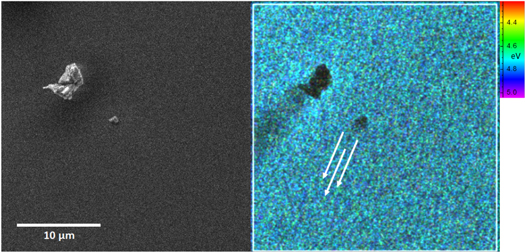
Figure 3. Color coded lateral distribution of the luminescence energy, recorded at 8 K and 5 keV PE energy.
Download figure:
Standard image High-resolution image
Figure 4. Series of DRCLS spectra taken at different primary electron energies. (T = 10 K)
Download figure:
Standard image High-resolution image
Figure 5. Difference spectra from the DRCLS series. The switching between the two contributions is clearly visible. The label on the right hand side marks the number of the pairs of spectra which were subtracted from each other.
Download figure:
Standard image High-resolution imageA reciprocal space map from x-ray diffraction (XRD) shown in figure 6 reveals that all quantum wells are lattice matched. From DRCLS it is obvious that there is a difference between the individual QWs, and because lattice matching is retained, either the lower quantum wells must contain less gallium, or their thickness must be reduced. Assuming a nominal quantum well thickness of 3 nm for now, the two peaks would correspond to 45% Ga and 41% Ga content, respectively, resulting from the numerical calculations described in section 2.2. Both, decreasing width of the QW or increasing Ga content, increase the emission energy and cannot separately be determined from the optical spectra alone.
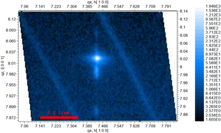
Figure 6. Reciprocal space map from XRD. The bright spot represents the AlN bulk material. Since the satellite peaks are aligned vertically under the AlN signal, the QWs are lattice matched.
Download figure:
Standard image High-resolution imageFigure 7 shows the lateral distribution of the 4.65 eV and the 4.8 eV luminescence measured with 1 and 5 kV acceleration voltage. The images have been smoothed by a Gaussian blur, contrast and brightness have been enhanced (similar to all images) in order to make the luminescence patterns better visible. The maps of the 4.65 eV luminescence band have a similar spatial distribution at 1 and 5 keV excitation energy, only the signal to noise ratio changes. There are some dark spots in the lower right quarter of the image, which stay dark even for the higher excitation energy. While the monochromatic CL map of 4.80 eV recorded at 1 keV PE energy consists mainly of noise, the map taken at 5 keV PE energy shows a clear lateral distribution, which only slightly differs from the one of 4.65 eV. These findings correlate with the speckles coded in blue color in figure 3. In summary, the 4.65 eV contribution is mainly homogeneously distributed for both excitation energies, while the 4.80 eV luminescence only contributes to the spectrum for high excitation energy. We therefore deduce that the high energy contribution at 4.8 eV originates from lateral inhomogeneities of the deeper lying QWs.
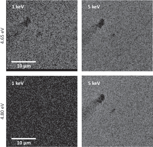
Figure 7. Comparison of the lateral distribution and intensity of the 4.65 and 4.80 eV luminescence measured with 1 and 5 kV acceleration voltage. For 1 kV, the 4.80 eV signal consists mainly of noise, while at 5 kV a clear luminescence map can be observed.
Download figure:
Standard image High-resolution imageTo evaluate which quantum wells are mainly contributing to the additional 4.80 eV band, the CL signal was evaluated with a corresponding simulation of the excitation at different electron energies. For a precise simulation, the sample structure was modeled with the stacking sequence determined by TEM as input. Figure 8 shows a cross-sectional TEM overview image of the quantum well stack. The white arrows ending at the sample surface indicate the growth direction. The five QWs are clearly resolved as dark stripes in this image. The cap layer nominally 30 nm thick was found to be actually only 25 nm. Figure 9 contains high resolution TEM images of the quantum wells in both HRTEM and HAADF mode. The fringes of the c plane can clearly be seen. The inset shows 2D power spectra obtained from the 2D FFT of the HRTEM image, clearly exhibiting the 0002 and the weaker 0004 reflection. Below, the corresponding selected area electron diffraction (SAED) pattern can be seen. The high-angle angular dark field (HAADF) image on the right also shows fluctuations of the quantum well thickness. An average thickness of 1.7 nm for the QWs and 8.3 nm for the AlN barriers was measured from the HRTEM image and was used for the simulation of the PE scattering and CL excitation.

Figure 8. Overview TEM images with two lamellas. The white arrows indicate the growth direction of the vertical structure, ending at the surface.
Download figure:
Standard image High-resolution image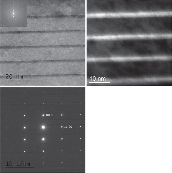
Figure 9. Left: HRTEM image of AlGaN quantum wells. Sample oriented along the  zone axis. The QWs are visible as dark contrasts. Inset: 2D power spectra obtained from the 2D FFT of the HRTEM image. Right: HAADF image in higher magnification. Lower image: Corresponding SAED pattern showing the orientation of the sample.
Download figure:
Standard image High-resolution imageThese values are now used as input for a Monte-Carlo simulation of the excitation volume, following the model described in section 2.1. We assume, that the CL emission intensity for the given layer under the surface is determined by the total energy deposited in the respective layer. The CL profile as a function of depth calculated this way is shown for some relevant PE energies in figure 10. These profiles reproduce the findings from the spectra series in figure 4 well. For 1 kV, only the first QW is expected to significantly contribute to the luminescence spectrum. When the PE energy is increased to 1.5 keV, the upper three QWs should dominate the spectrum. A comparison with the difference spectra in figure 5 shows, that for this excitation energy the higher energy parts of the spectrum start to contribute very weakly to the spectrum. Switching to 2 keV results in a stronger increase of the higher energy contribution. For 2 keV all five quantum wells should contribute simultaneously to the overall spectrum. The dashed profiles in figure 10 represent the expected CL intensity distribution when longer diffusion length around the quantum wells is assumed. The confinement of the excited carriers to the QWs is reduced, but the depth distribution of the generated luminescence shows the same tendency: For 1 keV, the CL signal is mainly generated at the position of the first QW, whereas at 2 keV all five quantum wells are excited. From this comparison between experiment and Monte-Carlo simulation we can conclude that the upper two quantum wells must significantly differ from the lower three. Therefore, these lower three QWs are responsible for the blue-shifted luminescence contribution in the overall spectrum, which is excited for higher PE energies. These findings also agree with the CL maps in figure 7, where the higher energy contribution does show a clear and structured signal only for higher acceleration voltages.
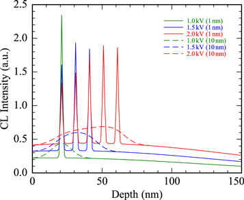
Figure 10. CL intensity profile calculated from the simulation of the PE scattering for two different effective diffusion length at the QWs.
Download figure:
Standard image High-resolution imageThese findings could be confirmed by further evaluation of the TEM data. The HAADF image in figure 9 shows, that the lower interfaces of all quantum wells are not as sharp as the upper ones. Lateral potential fluctuations due to the varying thickness of the QWs evolve from these inhomogeneities. Furthermore, the lower three QWs seem to exhibit a reduced average thickness. To ascertain whether this reduced thickness or a higher Al content (or lower Ga content, respectively) is responsible for the blue-shift, each QW was separately investigated using electron energy loss spectroscopy (EELS) in STEM mode, aiming at the determination of an approximate Al content. Figure 11 shows the HAADF reference image and the 179 spectra recorded along the orange line. Each pixel row in the lower spectral image corresponds to one spectrum. The intensity is brightness coded. To measure the absolute sample thickness for each quantum well, the log-ratio function of Malis et al was applied [32]. EELS spectra were recorded between 0 and 180 eV. For Al semi-quantification, the edge of the 73 eV of Al was chosen. To improve background fit and cross section agreement, the 'remove plural scattering' function of DigitalMicrograph was applied before final quantification. The ratio of zero-loss electrons to the total transmitted intensity t/λ was 1.3, which is a little high for quantification. Therefore, the Al content is shown in figure 12 without error bars because only a statistical error of about 10% is available (obtained by quantification tool Gatan Digital Micrograph Suite). For a quantitative measurement of the element content the sample is too thick and the effect of systematic errors such as multiple inelastic scattering, beam broadening of the probe etc are not included. However, the aluminum profile clearly shows a trend and demonstrates the presence of 5 QWs. Therefore, even without exact quantification the EELS data is meaningful and supports the other experimental data. This seems to contradict the findings of depth-resolved CL at first glance, which finds that the deeper QWs locally emit at higher energies, which would require larger Al content. From these results, we deduce that the reduced thickness and the thickness fluctuations of the lower three QWs must be overcompensated by their higher Ga content (lower Al content, respectively), resulting in the additional high energy contribution in the overall luminescence band. To evaluate these fluctuations further, two gray scale profiles were extracted from the HAADF image. Figure 13 shows the square-root of this ADF intensity profile [33]. The peaks in the ADF intensity profile corresponding to the bright stripes of the QWs in the HAADF image exhibit different full width at half maximum (FWHM) at the two positions. While the upper two QWs (0–20 nm) are roughly congruent with each other, the lower three QWs show a reduced FWHM for the blue profile. For a fixed composition, this narrowing of the QW width should result in a blue shift of the corresponding luminescence energy. This comparison of the local QW thicknesses is another indication that the lower QWs show pronounced thickness fluctuations. These findings are in good agreement with the DRCLS results. So local thickness variations, especially of the lower QWs can be identified to cause the high energy contribution to the QW luminescence spectrum.

Figure 11. HAADF reference image and corresponding EELS spectra. The 179 spectra were recorded along the orange line. The yellow box denotes the reference for drift correction. There is a clear signal contrast from all five quantum wells.
Download figure:
Standard image High-resolution image
Figure 12. Relative aluminum content of the five QWs determined by EELS, normalized to the upper most QW.
Download figure:
Standard image High-resolution image
Figure 13. Square root of the gray scale profile from top to bottom extracted form the HAADF image. There are clear local thickness fluctuations. The inset shows the HAADF image with lower magnification and the position of the profiling.
Download figure:
Standard image High-resolution image
6. Conclusions
We explore here the possibilities of depth-resolved CL measurements using fine steps in primary energy to resolve inhomogeneities in a stack of nominally identical quantum wells in the AlGaN/AlN material system. In combination with Monte-Carlo simulations and TEM micrographs, we can show specifically that the topmost two QWs differ from the lower lying ones in terms of Ga content and thickness fluctuations. DRCLS shows that these lower QWs show a more inhomogeneous luminescence distribution and are therefore responsible for the observed high energy shoulder in CL. While TEM is a very powerful tool to characterize small volumes of the sample with very high resolution, DRCLS can provide information on a comparably larger sample volume without additional sample preparation. The measurement demonstrates the ability of depth-resolved cathodoluminescence to differentiate even between individual quantum wells under certain circumstances with a non-destructive technique.
Acknowledgments
We thank Benjamin Neuschl for technical support and the Deutsche Forschungsgemeinschaft (DFG) for financial support within the project 'Untersuchungen zur Epitaxie von AlBGaN-Heterostrukturen für Anwendungen in UV-LEDs', # TH 419/25-1, SCHO 393-31/1, and KA 1295/22-1.
Data availability statement
The data that support the findings of this study are available upon request from the authors.