

Abstract
The metal-graphene contact resistance is one of the major limiting factors toward the technological exploitation of graphene in electronic devices and sensors. High contact resistance can be detrimental to device performance and spoil the intrinsic great properties of graphene. In this paper, we fabricate back-gate graphene field-effect transistors with different geometries to study the contact and channel resistance as well as the carrier mobility as a function of gate voltage and temperature. We apply the transfer length method and the y-function method showing that the two approaches can complement each other to evaluate the contact resistance and prevent artifacts in the estimation of carrier mobility dependence on the gate-voltage. We find that the gate voltage modulates both the contact and the channel resistance in a similar way but does not change the carrier mobility. We also show that raising the temperature lowers the carrier mobility, has a negligible effect on the contact resistance, and can induce a transition from a semiconducting to a metallic behavior of the graphene sheet resistance, depending on the applied gate voltage. Finally, we show that eliminating the detrimental effects of the contact resistance on the transistor channel current almost doubles the carrier field-effect mobility and that a competitive contact resistance as low as 700 Ω·μm can be achieved by the zig-zag shaping of the Ni contact.
Export citation and abstract BibTeX RIS

Original content from this work may be used under the terms of the Creative Commons Attribution 4.0 licence. Any further distribution of this work must maintain attribution to the author(s) and the title of the work, journal citation and DOI.
1. Introduction
The isolation of graphene [1–3] in 2004 and, later on, of h-BN [4], phosphorene [5],  [6–14],
  [15–17],
  [18, 19],
  [20, 21] etc, has strongly attracted the interest of the material science community to the world of two-dimensional (2D) materials.
Graphene, the two-dimensional layer of carbon atoms arranged in a honeycomb lattice, is still one of the most studied 2D systems for the unmatched electron mobility, the remarkable current capability and thermal conduction, the relatively high optical absorption coefficient, the mechanical strength as well as the easy and low cost fabrication [22–27].
Graphene is commonly produced by exfoliation from graphite [28, 29], epitaxial growth on SiC [30] or chemical vapor deposition (CVD) [31, 32]. In particular, CVD produces uniform and large-scale graphene flakes of high-quality and is compatible with the silicon technology; therefore, it has been largely exploited to realize new electronic devices such as diodes [33–36], transistors [37–39], field emitters [40, 41], chemical-biological sensors [42, 43], optoelectronic systems [44], photodetectors [45–50] and solar cells [51].
Due to its gapless band-structure, with the valence and conduction bands touching each other at the so-called Dirac points, graphene originates ambipolar field-effect transistors with V-shaped transfer characteristics, dominated by a p-branch at negative and n-type conduction at positive gate voltage [52]. The ambipolar conduction can be an important feature for complementary logic applications; however, the limited on/off ratio caused by the absence of intrinsic bandgap is a significant obstacle and requires delicate material engineering for real applications [53–55].
Despite the several doping techniques available to tune the graphene conductivity and boost the performance of graphene transistors, a major problem remains the suppression of device on-current caused by the graphene/contact resistance [56]. Indeed, ohmic and low resistance contacts are important figures of merit for high frequency devices and the realization of stable and low-resistance contacts is still under intensive study [57–61]. The variation of the contact resistance,  is attributed to many different causes, related to graphene growth and number of layers, metal type and deposition process, quality of the metal graphene/interface, measurement conditions, etc.
Conventional ohmic contacts between graphene and various metals exhibit rather large contact resistance ranging from few hundreds to thousands  Studies have been conducted on various types of metal/graphene interfaces showing that the best contact resistances can be achieved with Ni and Cu contacts yielding
  as low as
  [62–65]. Although the choice of the metal type is an important ingredient for good quality contacts, recent researches have developed special techniques for the reduction of the contact resistance. The most successful strategies have been the modification of the contact area to increase charge injection through the graphene edges and the graphene etching under the contacts to favor the formation of dangling carbon-to-metal bonds. Contact resistances down to
  have been obtained in this way [63, 65–67]. Anzi et al [67] report that the under-contact graphene etching reduces the contact resistance both for Au and Ni/Au contacts. Smith et al [63] demonstrate a contact resistance dependence on the number of graphene cuts under the contacts. Similarly, Lisker et al [57] optimize the metal/graphene interface by incrementing the contact perimeter. A low contact resistance enables the study of intrinsic graphene properties and increases the performance of graphene devices. As the matter of fact, the contact resistance can be tuned by the application of a gate voltage (
 ), which modulates the carrier concentration of the graphene channel. In this scenario, the contact resistance becomes larger in correspondence of the Dirac points, where the graphene conductivity is suppressed [68, 69].
The temperature dependence of  in graphene devices is still a controversial topic. A conspicuous number of studies report discrepant results evidencing either a negligible dependence of
  on T or strong changes of contact resistance with temperature [70–72].
In this work, we investigate the effect of back-gate voltage and temperature on the contact and channel resistance and on the carrier mobility in graphene field-effect transistors with Ni contacts. We fabricate back-gate devices with multiple leads which we analyze by both the transfer length method (TLM) [73–77] and the Y-function method [78–80]. The complementary application of the two methods leads to a more robust estimation of the contact resistance and of the gate-voltage dependence of the carrier mobility. We show that the gate voltage modulates the contact and the channel resistance in a similar way but has negligible effect on the carrier mobility. We also find that the field effect mobility decreases with raising the temperature, which does not affect the contact resistance, but can induce a transition from a semiconducting to a metallic behavior in the channel resistance, depending on the gate voltage. Finally, we show that eliminating the detrimental effect of the contact resistance can result in more than 80% increase of the field effect mobility.
2. Materials and methods
Graphene synthesis has been performed on 200 mm Ge/Si substrates using Aixtron's Black Magic BM300T CVD tool. The synthesis was carried out at the deposition temperatures of  using
using  as source of carbon and
  mixture as carrier gas, at 700 mbar for 60 min Raman and micro-Raman mapping confirmed that the optimized fabrication process led to high quality, defect-free, and uniform graphene film over the whole wafer [57, 81]. The so-obtained graphene was then transferred on p-type doped Si
  capped with 100 nm
  layer, patterned in long stripes by electron beam lithography (EBL) and dry etching, and finally covered by PMMA to prevent damages. Ni metal contacts were sputtered using a 50 W low-power process after keeping the sample degassing in vacuum at pressure
  mbar for 24 h. An annealing in 1:2 mixture of hydrogen and argon at 580 °C for 30 min was applied to further reduce the specific contact resistivity. The devices consist of patterned graphene stripes contacted with several parallel leads, at gradually increasing distances (
 ). Structures with diverse combinations of the contact size, distance and/or shape, were fabricated and analyzed as well, with an example reported in figures 1(a), (b).

Figure 1. Optical images taken at (a) 50x and (b) 100x magnification, and (c) schematic of a device with zig-zag shaped contacts. (d) Schematic of the device, showing the metal  the contact
  and the channel
  resistances.
  is the transfer length, representing the distance over which most of the current
  flows between the contact and the channel.
Download figure:
Standard image High-resolution imageMeasurements at different temperatures were performed using a Janis probe station equipped with four metallic nanotips connected to the source-measurement units of a Keithley 4200 SCS (Tektronix Inc.), at pressure of  mbar. The metal contacts were used as the drain and source electrodes while the
  substrate as the back gate and the gate dielectric, respectively.
The schematic of figure 1(d) shows that the total resistance,  obtained from the
  (drain-to-source current versus drain-to-source voltage) curves measured in a two-probe configuration between two given contacts, includes the contributions of the metal resistance,
  the contact resistance,
  i.e. the resistance at the 3D-metal/2D-graphene interface, and the channel resistance,

The channel resistance can be written as

where  is the graphene sheet resistance in
  (
( ), W the width of the graphene stripe and
  the distance between the two chosen contacts. We can express the contact resistance in terms of the transfer length,
  that represents the distance over which most of the current (
 ) flows between the contact and the channel:
  [82]. Therefore, neglecting
  (order of magnitude lower than
  and
and  ), it results

Equation (3) is used to estimate  and
and  from the straight-line fitting of a
  plot (TLM plot). The intercept of the straight-line with the horizontal axis
  provides the transfer length. If
  is small compared to the size D of the contact, the current flows mostly through the edge of the contact (current crowding effect) and only the contact edge influences the carrier injection and the conduction in the graphene channel. In this scenario, there are only two possibilities to reduce the contact resistance: etching the graphene under the contact to increase the contact edges or increasing the perimeter of the edge, for instance using zig-zag shaped edges.
For two-probe configuration measurements, an alternative approach to estimate the contact resistance is the so-called Y-function method (YFM). The method includes the contact resistance in the expression of the transistor current  as a function of
  and
and  (the gate-to-source voltage) [79, 83]:

where  is the
  capacitance (
 for 100 nm
 is the field-effect mobility and
  is the gate voltage corresponding to the Dirac point, i.e. to the minimum of the
  characteristic of the graphene transistor.
The  derivative of equation (4) represents the transconductance

and the ratio

is the so-called Y-function. Y results independent of  while
while  depends linearly on
  with angular coefficient proportional to the contact resistance. Thus, the plots of
  versus
  can be exploited to obtain the mobility
  (which is not affected by the contact resistance) and the contact resistance
  respectively.
Finally, taking the derivative of the Y-function in equation (6) with respect to  we obtain the mobility unaffected by the contact resistance, which should be independent of

3. Results and discussion
A two-probe configuration is adopted to measure the transfer ( curve at given
  ) and output (
 curves at selected
  ) characteristics for different contact combinations. In figure 2, we report an example of such measurements for the
  wide and
  long graphene channel contacted with Ni leads of size
  and zig-zag shaped edges (see figures 1(a), (b) and the schematic of the device figure 1(c)).
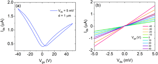
Figure 2. (a) Transfer and (b) output characteristics of a graphene transistor with  channel width and
  channel length.
Download figure:
Standard image High-resolution imageThe transfer characteristic (figure 2(a)) displays an asymmetric ambipolar behavior with a dominant hole branch and a current minimum (Dirac point) slightly above  The different slope of the two branches corresponds to the hole mobility (
 ) higher than the electron one (
 ), while the slight shift of the Dirac point to positive
  indicates a low p-type carrier concentration due to adsorbates and process residues such as PMMA, not removed by the 1 mbar vacuum and 400 K annealing [59, 84]. The hole-electron asymmetry is due to both unbalanced carrier injection from metal contacts and graphene interaction with the
  dielectric [84–89]. The interaction with
  is also the main cause of the hysteresis which appears when the gate voltage is swept back and forth [88–90]. The low mobility is also attributed to the fabrication process which needs further optimization. Figure 2(b) shows a linear
  behavior confirming the ohmic nature of the Ni/graphene contacts in the investigated voltage range. We intentionally limited the analysis to the triode region, as the achievement of a saturation regime would require operating the transistor at high drain bias and power dissipation, which would make the local temperature out of control.
Figure 3(a) shows the total resistance  measured between multiple couples of leads of the TLM structure, at room temperature and under different gate biases, ranging from −40 V to 40 V. The TLM curves display the linear behavior predicted by equation (3) and are used to extract
  and
and  as a function of the gate voltage
  (figure 3(b)). Both parameters exhibit a non-monotonic trend with maximum values (
 and
and  ) corresponding to the Dirac point (
 ), and a decrease when the back-gate dopes the graphene by attracting electrons or holes in the channel. We highlight that figure 3(b) demonstrates how the gate voltage affects the graphene layer not only in the channel region but also under the contacts, as previously reported [91].

Figure 3. (a) TLM plot and (b)  as function of the gate voltage. (c) TLM curves and (d)
  at
at  and
and  (inset) as function of the temperature.
Download figure:
Standard image High-resolution image
 extracted from the
  plot ranges between
  and
and  smaller the
  contact size, thereby confirming that the device works under the aforementioned current crowding regime.
Remarkably, comparison with a similar device contacted by straight contacts, i.e. no zig-zag edges, measured in the same conditions, exhibits  higher contact resistance (
 versus
  at
at  ), confirming the importance of increasing the length of the contact perimeter.
Similar measurements were performed as a function of the temperature, T, in the range 90 K to 400 K. The linear behavior of the  curves is preserved when the temperature is changed (figure 3(c)) but their slope decreases with increasing T. Figure 3(d) reports the temperature dependence of
  and
and  evaluated at
 remains constant over the 90–400 K temperature range while the graphene sheet resistance decreases, changing linearly from
  at 90 K to
  at 400 K with slope
  The independence of
  on the temperature is confirmed also when
  is evaluated at
  as shown in the inset of figure 3(d). Conversely, a new feature appears in the temperature behavior of
  at
at  the sheet resistance decreases until the temperature reaches
  and raises for
  up to
up to  at
at  Otherwise stated, a transition from a semiconducting to a metallic behavior occurs in graphene around
  consistently with what has been observed before [92–95]. Similar TLM analyses have been conducted on devices of the same chip with graphene channel
  or
or  wide or with different layout. The estimated contact resistance, normalized by the channel width,
  and sheet resistances are summarized in figure 4, showing a mean
  value of
  and
and  We note that, owed to the zig-zag geometry, the TZ structure in figure 4 (which is the previously analyzed one), shows a normalized contact resistance as low as
  at
at  within the range of the good quality contacts typically reported in the literature [63, 65–67]. Considering that the device-to-device fluctuations across the wafer are less than 30% [54], the improvement of the zig-zag geometry is highly significant. The differences in the sheet resistance shown in figure 4(b)) can be attributed to local variations of the transferred graphene foil and different damage induced by the fabrication process.

Figure 4. (a) Contact resistance normalized by the channel width and (b) graphene sheet resistance calculated for different TLM devices (TS = star configuration, TN = straight contacts, TZ = contacts with zig-zag edges).
Download figure:
Standard image High-resolution imageWe further exploited the TLM measurements to study the dependence of the field-effect mobility,  on the channel length
  and the temperature. The mobility was estimated from the slope
  of the linear part of the transfer characteristics as

Figure 5(a) shows the hole mobility as function of channel length, an increase of  with
with  appears for small
  with a further saturation at larger channel lengths.. Such a behavior can be expressed as
  where
where  is the saturated mobility and
  the mean free path [96]. From the fit of the experimental data, we obtain
 and
and  The saturation at channel length
  corresponds to the establishment of a diffusive transport regime, while the mobility degradation at lower
  (
( ) is an artifact due to the application of equation (8) in a regime where the transport becomes quasi-ballistic or ballistic [96, 97]. The influence of the temperature on the mobility, for the chosen device with
  is shown in figure 5(b), which indicates that most of the mobility degradation occurs for
  (
( from its value at
 ). This behavior can be understood considering that phonon scattering in graphene becomes relevant only at higher temperatures [98–100].

Figure 5. Hole field-effect mobility plotted as function of channel length (a) and temperature (b). Panel (c) shows the hole and electron mobilities as function of  at room temperature, for two channel lengths,
  (blue circles) and
  ( orange circles).The Y-function method has been successfully applied to eliminate the effects of the contact resistance on the estimation of the mobility and for the evaluation of
  itself. The mobility and contact resistance are obtained from the plots of
  versus
  as explained before (see equations (5) and (6)). An example of these plots is shown in figures 6(a) and (b) for the p-branch of the transfer characteristic of the device with
Download figure:
Standard image High-resolution imageThe electron/hole mobilities evaluated from the numerical derivative of the  curves according to equation (8), are plotted in figure 5(c) as function of
  (gate overdrive) for two channel lengths (1 and 10
  respectively). The mobilities show a minimum at the Dirac point, reach a maximum for increasing overdrive and decrease smoothly for
  The contact resistance, whose effect on the mobility is not eliminated in this type of analysis, could cause this decrease of
  with gate overdrive. To confirm such a hypothesis and obtain a more accurate
  versus
  behavior, we considered the Y-function method as complementary approach to the TLM analysis.
From figure 6(a), we obtained a field effect mobility  which together with the data in figure 6(b) yields
  (or
(or  ). These values are consistent with the results from the TLM analysis.

Figure 6. (a)  and (b)
  plotted as function of gate voltage using the Y-Function method. Comparison between
  versus
  extrapolated through the TLM method (light blue curves) and Y-function method (purple curves) for different the channel lengths
Download figure:
Standard image High-resolution image
The plots of the mobility versus  (figures 6(c) and (d) for
  and
and  channel lengths, respectively) show that
  is unaffected by
  and is independent of the gate overdrive. The elimination of the contact resistance effect by the YFM confirms that gate dependence of the field-effect mobility is only an artifact of the TLM method.
We also note from figures 6(c) and (d) that removing  results in significantly higher mobility, with over 80% increase.
4. Conclusions
In conclusion, we have fabricated and analyzed Ni-contacted graphene FETs and studied the back-gate and temperature dependence of the contact and channel resistance. We have measured devices with different geometrical structures and achieved competitive contact resistances using zig-zag shaped Ni contacts, also confirming the importance of contact geometry in the metal/graphene contact resistance.
We have found that the gate voltage modulates the contact and the channel resistance in a similar way but does not change the carrier mobility. We have also shown that raising the temperature decreases the carrier mobility, has a negligible effect on the contact resistance and can change the initial semiconducting behavior of the channel resistance into a metallic one, depending on the gate voltage. We used two complementary methods, namely the TLM and the YFM, to show that, eliminating the detrimental effect of the contact resistance, can almost double the carrier field-effect mobility.