
Abstract
In this study, in the first stage, an antenna with circular polarization was designed with the technique of cutting the corners of radiation patches. Then a hybrid structure with DGS and EBG methods was presented. For this purpose, the designed structure of the combination of DGS and EBG, which was designed to reduce mutual coupling, was placed between the radiating elements of the antenna. This method is implemented on a microstrip antenna. The reduction of the coupling of this structure is based on the creation of a magnetic band gap. All simulation was performed numerically by CST Microwave Studio software. The simulation results showed that this structure, unlike previous structures, improves all the characteristics of the antenna, such as the antenna gain, antenna radiation efficiency, and antenna envelope correlation coefficient. Also, the resonant frequency of the antenna is 6.35 GHz, which reduces the coupling by 36.5 dB by placing the designed structure between the radiating elements of the antenna.
Export citation and abstract BibTeX RIS
1. Introduction
The antenna is part of a telecommunication system that is responsible for sending and receiving telecommunication waves in the system. There are different types of antennas (spiral wire, reflective horn, phased array, microstrip, etc). MIMO (multi-input, multi-output) is a wave propagation technology (antenna) for wireless telecommunication systems, and it has found a special place in wireless telecommunications due to the significant increase in data throughput and telecommunication link range, without the need for additional bandwidth or additional transmission power [1–4]. If the antennas are placed next to each other in an array [5] (both in receiver and transmitter modes), an undesired coupling occurs between the two antenna radiators elements, due to the reciprocal coupling of electric fields [6] which is induced from the first radiating element to the second radiating element and causes current to flow on the second radiating element, which is called the undesired electromagnetic coupling effect of the reciprocating coupling [7]. This mutual coupling becomes important when the ratio of the thickness of the sublayer to the wavelength of the free space is  as indicated by relation (1) [8]:

where  is the thickness of the substrate,
  is the wavelength of the free space and
  is the relative permittivity or dielectric constant of the substrate.This effect depends on the type of antenna and its design parameters, the relative position of the elements in the array (the distance between the two antennas is inversely related to the amount of coupling between the two antennas), and the power supply of the array elements [9]. In a typical array, to properly isolate the radiators and the antenna, the distance between the radiators is at least
  But today, due to the compression and integration of the circuits, it is necessary to miniaturize the antennas. This can reduce the distance between the radiation elements and thus increase coupling between them [10].
This coupling causes changes such as changes in the radiation beam of the arrays, changes in the input voltage of the arrays, changes in the matching properties of the antennas, changes in the input impedance, and the creation of blind spots [11]. To date, various strategies have been considered to reduce coupling [12–20], including split-ring resonators (SRRs) [13], electromagnetic bandgap structures (EBGs) [14, 15], frequency selective surfaces (FSSs) [16, 17], defected ground structures (DGSs) [18], and photonic bandgap structures (PBGs) [19, 20]. To produce circular polarization, many structures with different properties have been proposed [21].
Among the advanced structures that minimize mutual coupling are split ring resonators [22], EM bandgap [23, 24], frequency selective surfaces [25, 26], shaped elements [27], defected ground structures [28–31], polarization-rotator wall [32], automatically designed parasitic elements [33], indirect coupler [34], and photonic bandgaps [35]. An antenna-to antenna mutual coupling mitigation method using stepped-impedance converters is also explored [36]. Furthermore, the use of parallel microstrip patch lines in a configuration that allows for proper isolation has been proposed by one recent study of dual-functional MIMO antennas [37]. For 3D antenna arrays, feedforward current has been proposed to mitigate mutual coupling [38].
In the practice of communication channels, there are many obstacles and electromagnetic waves reach the receiver from different directions. The waves that reach the receiver antenna directly differ from the waves that reach the receiver antenna due to reflection in terms of amplitude and phase, and cause interference in the receiver, which is called tach. Using circular polarization antennas, the waves change their direction of polarization due to reflection, i.e. if they are upright, they turn left after reflection, and vice versa, multi-directional interference is reduced. Also, unlike linear polarization antennas, which must be in the same direction to have a reliable connection between the transmitter and receiver, circular polarization antennas send and receive both horizontal and vertical components. Therefore, the direction of the antennas in the receiver and transmitter is not important. So.in this research, a structure has been used that, while having the necessary specifications, the antenna manufacturing process is simple and the mass production of the antenna is simple and low cost according to the available facilities.
2. Description of the designed antenna
The analysis of various electromagnetic structures including antennas using analytical and numerical methods has attracted the attention of many researchers. In general, the methods of analyzing electromagnetic problems can be divided into two categories including differential equations or integral equations.Each of these methods has advantages and disadvantages, and its calculations are difficult and complicated, for this reason, the results are analyzed by using appropriate meshing and diagram analysis in the software.
The use of circular polarization due to its attractive properties such as overcoming the multi-way phenomenon, no need to fine-tune the transmitter and receiver antennas, reuse of frequency band using left and right, solving Faraday rotation problem in satellite communications and etc, has more important than linear polarization [7]. Hence it is used in many telecommunication systems. This feature also reduces the effectiveness of mobile communications due to climate, so circular polarization is used today in various military and industrial applications. For this purpose, a square patch with a pair of cut corners is used to produce circular polarization, which is fed by a probe through a coaxial line. Antenna power supply with coaxial line has advantages over micro-line power supply. The most important of these advantages are lower power line losses, prevention of undesirable power line radiation and the ability to adjust the input impedance by changing the power supply (without the need for a quarter wavelength line). The patch is made on a 6035 RT microwave substrate with a dielectric coefficient of εr = 3.6 and a dielectric thickness of 1 mm made by Rogers Company. The antenna resonance frequency is about 6.39 GHz, which is in the C-frequency band and is powered by a 50 ohm coaxial SMA probe. Also, all the dimensions of this antenna were calculated and designed according to the standard formulas presented in [9]. Figure 1 shows the structure of the designed antenna. The antenna is fed by a probe through the coaxial line and the radiant fields of the antenna have a right circular polarization. If the cut is made on the other two corners, left circular polarization will be produced. According to the resonator model, the predominant mode in the square patch is 10TM. In order to produce circular polarization, it is necessary to stimulate the 01TM mode as well. This is done by making cuts in the two corners located on the diameter of the patch. If the square dimensions and the amount of cut are selected properly, two modes with equal amplitude and phase difference of 90 degrees will be created, which will intensify at two frequencies close to each other. In this case, at a frequency equal to the numerical mean of the resonant frequency of these modes, the phase difference between the two modes is exactly 90 degrees and the amplitude of the modes is equal [39]. The power supply must also be adjusted so that the impedance resonant frequency is equal to this frequency. The amount of patch corners cut depends on the quality factor (Q0) of the square patch. The quality factor is also a function of the dielectric characteristics and dimensions of the patch. It should be noted that the feeding position also affects the amplitude of the excited modes and therefore the amount of cutting surface and the feeding location both affect the phase difference between the two modes. Therefore, after the initial design and analysis of the antenna, it is necessary to change the power supply or the amount of cut, the necessary optimization to achieve the desired parameters. If the area of the cut sections in the corners of the patch is denoted by ∆S, the value of ∆S and the resonant frequency of the excited modes are [40]:

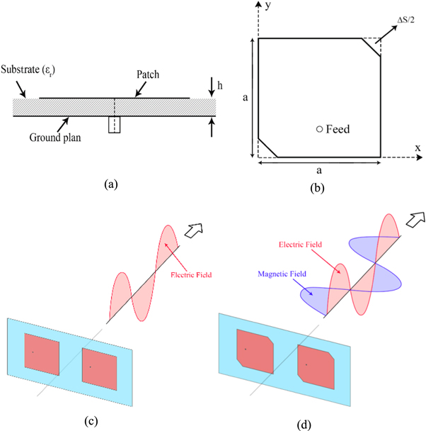
Figure 1. (a) Top view of the antenna patch designed with circular polarization, (b) Side view of antenna components, (c) Antenna polarization display before cutting the corners of the radiation patches (linear polarization), (d) Antenna polarization display after cutting the corners of the radiation patches (circular polarization).
Download figure:
Standard image High-resolution imageIn equation (2), f0 is the resonant frequency of the square patch without cutting, ∆S is the total amount of the cutting surface, S is the surface of the patch without cutting, and Q0 is the quality factor of the square patch without cutting, which depends on the substrate material and +thickness. f1 and f2 are the frequencies of excited modes whose numerical mean will be the circular polarization frequency.
First, according to this central frequency and the characteristics of the substrate used, the length of the square patch (a) can be calculated approximately according to equation (3) [41]

Where:


Where c is the speed of light in open space and h is the dielectric thickness. In order to calculate the amount of cut corners using equation (2), it is necessary to know Q0.

Analytical calculation of Q0 is not simple, but it is possible to determine the bandwidth of the antenna by simulating the antenna using cst microwave studio software according to the S and VSWR charts [40]. After determining the amount of cutting corners, it is necessary to determine the antenna power supply. To have a circular polarization in figure 1(a) and (b), the feed point in the x direction must be in the middle of the patch. Shifting the power supply in the y direction changes the input impedance of the antenna. The closer the power supply is to the edge of the antenna, the higher the real input impedance. By analyzing and simulating the antenna by software and observing the changes in input impedance in the Smith chart, it is possible to adapt the antenna to the line of 50 ohm at the desired central frequency by changing the power supply or other parameters, so that the circular polarization frequency Also correspond to the central impedance frequency. Figures 1(c) and (d) show the vector type of radiation polarization from the antenna.
2.1. Array antenna
In general, the radiative property of an array antenna is determined when its aperture is determined. The amplitude and phase in each element are usually determined by the expected application, such as weak sub-beams or beam orientation. The means of stimulating the radiation elements is an important factor that must be carefully considered in order to achieve the desired distribution for the desired application. The feed networks of microstrip patch array antennas can be broadly categorized into parallel and series feed network.
Parallel network: consists of a single input and several power lines that form parallel outlets. Each of these feed lines terminates in radiation elements [42].
Series network: The second type of network is the series power supply network, which usually consists of a continuous transmission line that transmits part of the energy exponentially to the radiation elements, which receive energy in various ways such as direct coupling or valve. Both feedings can be considered flat with radiant elements or on a separate transmission line [42].
The reason for mutual coupling are electric fields that are induced from the first patch to the second patch and cause current to flow to the second patch. There are two types of microstrip patches, one in the y direction and the other in the 'x' direction (figure 2). The purpose of the field placed by adjusting the supply lines along L is to generate a linear electric field of radiation in intensification along 'y'. This means that the radiated electric fields are further polarized along y, and this also means that there is more coupling in this state. As a result, this position indicates that picking the patch along the x reduces cross-tapping. In this paper, in order to prove the effect of structures designed to reduce mutual coupling, the y-directional arrangement, which has more reciprocal coupling, has been used. Figure 3 shows the antenna design example and table 1 shows the antenna dimension values.
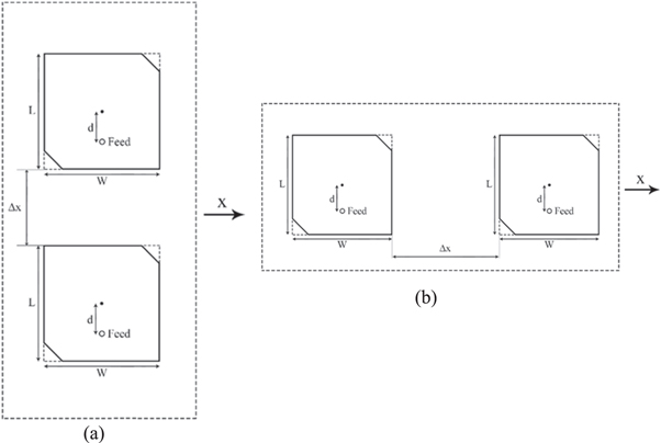
Figure 2. (a) Top view of antenna patch array in X direction, (b) Top view of antenna patch array in Y direction.
Download figure:
Standard image High-resolution image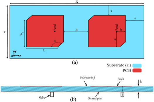
Figure 3. Initially designed antenna view without placement of the coupling reduction structure, (a) Top view, (b) Side view.
Download figure:
Standard image High-resolution imageTable 1. Values of designed antenna dimensions figure 3.
| Parameter | Dimension (mm) |
|---|---|
| X | 70.7 |
| Y | 35.4 |
| c | 11.7 |
| f | 11.7 |
| W1 | 10.6 |
| L1 | 10.6 |
| D | 23.5 |
| A | 5.8 |
| b | 3.3 |
| θ | 135° |
| h | 1 |
To investigate the effect of mutual coupling between the two elements of the array antenna, the scattering parameters of S12 should be analyzed before and after applying the reduction structure. In order to evaluate the amount of cross-coupling in the first step, figure 4 shows the diagram of the antenna scattering parameters before placing the coupling reduction structure. According to diagram S11 in figure 4, the antenna resonance frequency is 6.35 GHz in the C-frequency band. The C-frequency band is in the frequency range of 4 to 8 GHz. This band is the first frequency allocated for communication between the Earth and satellites, and it is mostly used in commercial communication satellites. Also, to study the type of polarization of the antenna, the axial ratio diagram should be examined. When the value of axial ratio in the designed antenna resonance frequency is less than 3 dB, it means that the polarization of the antenna is circular, which is shown in figure 5 in the diagram of the axial ratio of the designed antenna in terms of frequency. According to equation (7), the designed antenna bandwidth is 0.5%.

The characteristics of the radiant pattern of the initially designed antenna are shown in figure 6. Figure 6 shows the simulated E-plane radiation pattern at a 6.35 GHz antenna resonant frequency without mutual reduction structure with a maximum value of 10.4 dB.
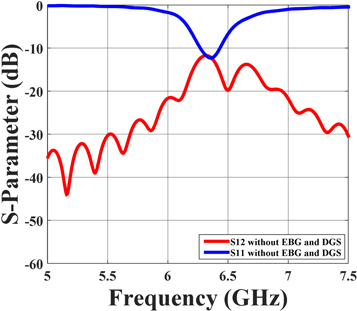
Figure 4. Diagram of antenna scattering parameters without EBG and DGS structure.
Download figure:
Standard image High-resolution image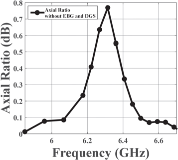
Figure 5. Axial Ratio diagram of antenna without EBG and DGS structure.
Download figure:
Standard image High-resolution image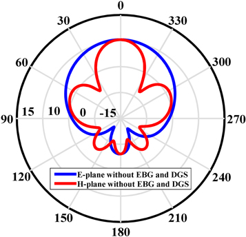
Figure 6. Antenna radiation pattern diagram without EBG and DGS structure.
Download figure:
Standard image High-resolution image3. Describe the structure designed to reduce mutual coupling
EBG structures have provided promising paradigm for novel antenna designs. Due to the complexity of the EBG structures, it is usually difficult to characterize them through purely analytical methods. Instead, full wave simulators that are based on advanced numerical methods have been used in EBG analysis. Dispersion diagram, surface impedance, and reflection phase features are revealed for different EBG structures. These analysis tools have been integrated with modern optimization techniques such as genetic algorithms and particle swarm optimization to synthesis unique EBG structures.
EBG structures can prevent and block the transmission of electromagnetic waves at a certain frequency, or be considered as a structure for the transmission of electromagnetic waves [43]. Stop-band, pass-band, and band-gap can be specified with EBG structures [44]. The structure of EBG is a repetition period of elements of dielectric or metallic materials, which are designed as a unit cell and are placed together with a certain repetition. By adjusting the repetition shape of the unit cell and the resonance value of the unit cell, many and different band gaps can be created [45]. It also provided an EBG structure with inductance and capacitance properties. Therefore, the phase constant of an electromagnetic wave distributed under the patch will be much higher than the transverse electromagnetic mode, and as a result, the EBG structure operates in a slow wave environment with a shorter wavelength than the transverse electromagnetic mode. Typically, the EBG structure is placed between the antenna arrays. Also, DGS refers to the act of creating defects in the ground plane [46]. EBG is a method to improve many characteristics of MIMO systems [47]. Also, EBG plays a significant role in reducing mutual-coupling and can increase reflected radiation [48, 49]. In order to achieve the desired electromagnetic forbidden band, it is possible to create a gap in the ground plane in different shapes and designs. The EBG created in the ground plane controls the current in the ground plane by reducing the interference between the adjacent elements and reduces the mutual coupling between the radiating elements.
In this paper, a combination of EBG and DGS methods is used to reduce mutual coupling to design a new structure. The structure of the EBG consists of several nested circles, and the structure of the DGS consists of a section of the ground plate with two circular rings, which is shown in figure 7 of the unit cell view of the designed structure. Table 2 also shows the dimensions of the designed structure in figure 7. In this study, in order to analyze the structure and obtain the magnetic band gap, Eigenmode method and Dispersion Diagram extraction have been used. One of the things to keep in mind about this method is that the structure is alternating on both the X and Y axes, and the accuracy of this method is reduced for structures that are only alternating in one direction or have a large number of rotations. Figure 8 shows the output of the Dispersion Diagram or PBG curve from the CST Microwave Studio software for the composite structure of figure 7. The yellow area represents the magnetic band gap of the structure and the horizontal diagram is ΓΧΜΓ, the interval [0,1] or [Γ Χ] represents the electrical phase [0,180] degrees. From figure 8, two points are important, first, that the inner area of the light cone is used to determine the band gap, and second, that the mode1 curve is ignored in the band gap calculation. The second point is not considering one of the modes, and the qualitative answer to this disregard can be found by examining the shape of electric fields at one of the values of kx (first Brillouin region (ΓΧ)) in the inner area of the light cone and the YZ plane (according to the structure) determined. Since in this paper the combined structure of EBG and DGS has been investigated for application of coupling reduction in flat array antennas and we know that the electric field vectors inside the substrate are in the ±Z direction and the dominant direction of the vectors in one direction.(For example, all are in the −Z direction). In other words, for the Y axis, there is an expectation of even symmetry for the electric field vectors within the substrate. Therefore, according to the above points, only the first mode is out of this rule and it can not be included in the calculation of Band Gap (figure 8).
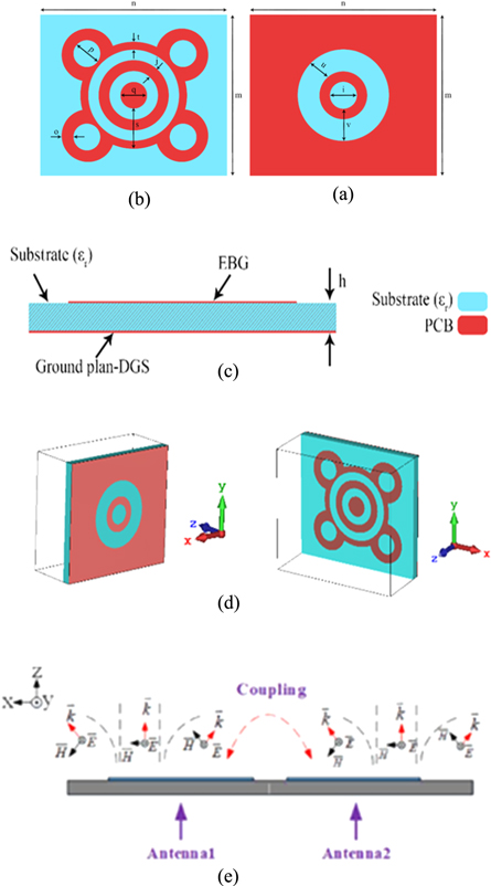
Figure 7. View of the cell structure of the combined DGS and EBG unit to reduce mutual coupling, (a) DGS bottom view. (b) Top view of EBG, (c) Side view, (d) Three-dimensional view, and (e) Radiation field distribution of two antenna radiation elements.
Download figure:
Standard image High-resolution imageTable 2. Unit cell values of figure 7.
| Parameter | Dimension (mm) |
|---|---|
| n | 14 |
| m | 12 |
| t | 0.6 |
| j | 0.8 |
| p | 2 |
| q | 2 |
| s | 3 |
| o | 0.8 |
| u | 1.6 |
| i | 2 |
| v | 2.4 |

Figure 8. Dispersion Diagram output diagram in order to obtain the magnetic band gap of the structure.
Download figure:
Standard image High-resolution imageDispersion Diagram output (figure 8) shows that the magnetic gap band of the structure designed in this study is between 6 GHz to about 7.8 GHz, which means that in this frequency range, there is a magnetic band for the designed structure, and in this frequency range, only coupling reduction is applied. Therefore, it is not used in other frequencies. But by considering the application of the working frequency of the antenna and considering the inverse relationship between the frequency and the dimensions of the structure, different working frequencies can be achieved by changing the dimensions of the structure. So that by reducing the dimensions of the structure, a higher working frequency can be achieved and by increasing the dimensions of the structure, a lower working frequency can be achieved. Therefore, it can be concluded that a special design must be done for each frequency range.
4. Final results
According to the contents and designs of sections 2 and 3, in this section, by placing the combined structure of EBG and DGS designed, the results of mutual coupling between array antenna elements were analyzed. Figure 9 shows the antenna with coupling reduction structures between the two radiating elements of the antenna.

Figure 9. Placement of the structure designed for mutual coupling, (a) Underside view of the DGS structure antenna. (b) Upper view of EBG structure antenna.
Download figure:
Standard image High-resolution imageAlso, figures 10 and 11 show a comparison diagram of the scattering parameters and the radiation pattern of the antenna before and after the placement of the structure designed to reduce the mutual coupling between the elements of the array antenna, respectively. In figure 10, three stages of the effect of the number of repetitions of the unit cell among the antenna patches were investigated. According to the graphs of dispersion parameter S12 in figure 10, the best case for unit cell repetition between patch antennas is STEP3 (4 unit cell repetitions), which applied a 36.5 dB mutual coupling reduction circuit. Also, a comparative diagram of the Axial Ratio antenna without and with EBG and DGS structure is shown in figure 12.
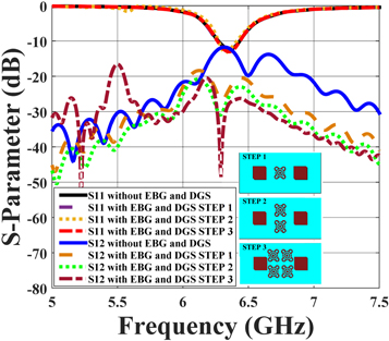
Figure 10. Diagram of antenna dispersion parameters without and with EBG and DGS structure in three STEPs with different arrangement of unit cell.
Download figure:
Standard image High-resolution image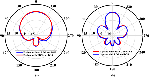
Figure 11. Comparative diagram of unstructured antenna radiation pattern with EBG and DGS structure. a) H-plane b) E-plane.
Download figure:
Standard image High-resolution image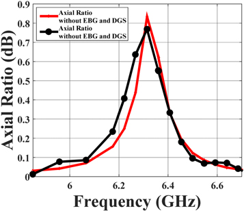
Figure 12. Comparative diagram of Axial Ratio antenna without and with EBG and DGS structure.
Download figure:
Standard image High-resolution imageThe analysis of figure 11 shows the increase in antenna gain from 10.4 dB to 10.9 dB. A comparative diagram between antenna radiation efficiency before and after the EBG and DGS structure (figure 13) shows that the antenna radiation efficiency improves 7.1%.
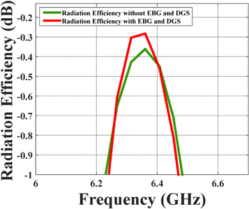
Figure 13. Comparative diagram of Radiation Efficiency of antenna without and with EBG and DGS structure.
Download figure:
Standard image High-resolution imageEnvelope Correlation Coefficient (ECC) is an important merit for any active multi-input multi-output (MIMO) antenna system that can be measured and calculated using complex patterns (equations (8) and (9)) [50]. The comparative diagram in figure 14 shows the ECC diagram before and after the placement of the EBG and DGS structures, which shows the improvement of the diagram after the placement of the EBG and DGS structures compared to before the placement of the EBG and DGS structures. The closer the ECC value is to zero, the better the ECC value. This improvement increases channel capacity and increases diversity gain.


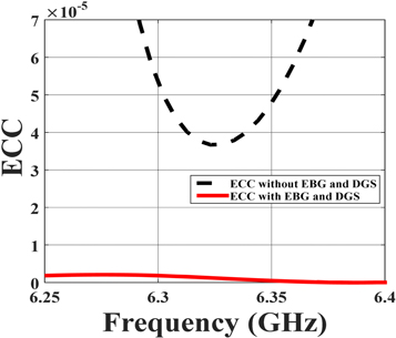
Figure 14. Comparative diagram of Envelope Correlation Coefficient antenna without and with EBG and DGS structure.
Download figure:
Standard image High-resolution imageThe main factor of mutual coupling is the transfer of surface currents from the first patch to the second patch. Figure 15 shows the distribution of surface currents in an antenna with a coupling reduction structure and without a coupling reduction structure between the two antenna radiation elements. Figure 15 shows how the structure designed to reduce mutual coupling acts as a barrier by stimulating one of the patches and prevents the transfer of surface current from the first patch to the second patch. Also in figure 16, magnetic fields of the antenna with the coupling reduction structure and without the coupling reduction structure between the two radiating elements of the antenna is shown. Table 3 shows a comparison between the studies of others and the study done in this article. By comparing the results of table 3, the amount of reduction of mutual coupling in this study shows a favorable value compared to the studies of others.
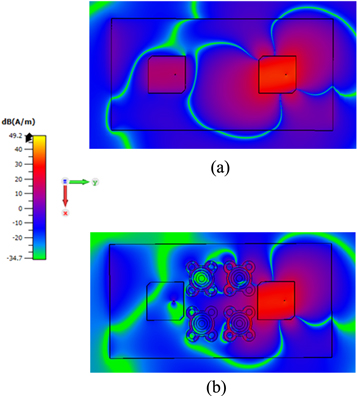
Figure 15. Distribution of antenna surface currents (a) without EBG and DGS structure (b) with EBG and DGS structure.
Download figure:
Standard image High-resolution image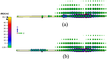
Figure 16. Antenna magnetic fields (a) without EBG and DGS structure (b) with EBG and DGS structure.
Download figure:
Standard image High-resolution image
Table 3. Comparison results of studies of others and this study.
| Freq.(GHz) | Size^ | Isolation value (dB) | Gap* | Method | Achievements | Application | References |
|---|---|---|---|---|---|---|---|
| 7 |

| 15 |

| Confined water | Wide coupling reduction + improving S11 | Aerial/naval multifunctional devices | [50] |
| 60 |

| 10 |

| EM bandgap | Reduced size | Wireless systems | [23] |
| 6.5 |

| 14 |

| EM bandgap | 14 dB coupling reduction | × | [24] |
| 30.5 |

| 10 |

| FSS superstrate | Circularly polarized antenna | × | [26] |
| 2.5/4.5 |

| 20 |

| Defective ground | Dual frequency band | Wireless systems | [28] |
| 10 |

| 20 | >Size | Defective ground | 20 dB coupling reduction | Amateur radio/satellite | [31] |
| 60 |

| 16 |

| Polarization rotator | 16 dB coupling reduction | Wireless systems | [32] |
| 2.5/3.4 |

| 7 |

| Parasitic elements | Automatically designed | Array antennas | [33] |
| 10 |

| 30 |

| Indirect waveguide coupler | 30 dB coupling reduction | X-band | [34] |
| 10 |

| 12 |

| Metamaterial bandgap | High number of array elements | × | [35] |
| 2.5/5.25 |

| 8 |

| Impedance converter | Dual frequency band | Wireless terminal | [36] |
| 4.4 |

| — |

| Microstrip patch lines | Dual-functional device | Beamforming network | [37] |
| 6.35 |

| 36.5 |

| DGS and EBG | Gain improvement, antenna Radiation Efficiency improvement and antenna ECC improvement + 36.5 dB coupling reduction | Array antennas C-band | This work |
^: Presents the coupling reducer dimension.-: No isolation improvement goal has been set.*: Edge-to-edge gap between adjacent radiating elements×: There are no application suggestions in the related work.
5. Conclusion
In this paper, first, a circular array antenna was designed with the technique of cutting the corners of the patches. Then, by combining EBG and DGS methods, a single cell was designed to reduce mutual coupling. Due to the fact that in previous studies, the combination of the two methods did not reduce the coupling in the antenna with circular polarization at a frequency of 6.3. Therefore, by applying a combination of EBG and DGS methods, the reduction of mutual coupling by 36.5 dB was calculated, which is an acceptable value compared to previous studies. The advantages of this structure include improved antenna gain, antenna radiation efficiency, and antenna envelope correlation coefficient. This structure can be used in all transmitter and receiver systems to send waves from the ground to the satellite in telecommunication and military satellites in the C frequency band. In less research, all antenna components have been improved together, and by designing this combined structure, the characteristics of all antenna components have been improved. This structure can be used in aperture array antennas and wherever there is a need to suppress surface waves in the frequency range of 6 to 7.8 GHz. Also, by changing the dimensions of the main elements of the designed unit cell, its band gap frequency can be changed and this structure can be used in other frequencies.
Conflict of interest
The authors declare no conflict of interests.
Author contribution in the manuscript
All authors contributed to the study conception and design. Data collection and analysis were performed by A Shirpay, M R Rohaninezhad, M Tavakoli, E Zarezadeh. The first draft of the manuscript was written by A Shirpay and all authors commented on previous versions of the manuscript. All authors read and approved the final manuscript.