
Abstract
We propose a hybrid gap plasmonic traveling wave amplifier (TWA) with electrically pumped multiple quantum wells (MQW). This TWA has deep sub-wavelength mode field scale and works at 1310 nm window. For the polarization-independent amplification we design the InGaAlAs tensile-strain MQW. Furthermore we analyze this plasmonic TWA's optical, electrical and thermal characteristics by finite element method. First we get the suitable trade-off point between the affordable mode propagation loss and moderate mode field size by adjusting the gap width and height. Second we find that the narrower the MQW, the higher the MQW local gain. Third, our device has good thermal performance as the plasmonic wave power is less than 5 μw. Simulation results suggest that the independent polarization gain appears at 1317 nm wavelength. At this wavelength 3.60 cm−1 mode gain and 161 nm mode width are obtained as the 9.39 kA cm−2 injection current and 10 nm × 240 nm gap size.
Export citation and abstract BibTeX RIS

Original content from this work may be used under the terms of the Creative Commons Attribution 4.0 licence. Any further distribution of this work must maintain attribution to the author(s) and the title of the work, journal citation and DOI.
1. Introduction
The deep sub-wavelength scale plasmonic components are being developed for realizing compact photonic integrated circuits(PIC). But with the plasmonic wave field size compressed, its high propagation loss rises up to be the main obstacle.
For overcoming this problem, two ways are being explored. One is to look for the low loss medium for the plasmonic component [1, 2], and the other one is to compensate the mode propagation loss by the active gain medium.
For effectively compensating the loss, various structures and gain media are proposed to construct the plasmonic amplifiers, such as the DLSPP with Schottky junction [3], the gap plasmonic double heterostructure [4–9] and so on.
In exploring the different plasmonic waveguide structures, people find that there is a trade-off between the plasmonic mode field size and its propagation loss. In the dielectric/metal and metal/dielectric/metal structure when the plasmonic mode field is significantly confined, its propagation loss is so high that it will be difficult to compensate this loss [10].
Therefore the hybrid gap plasmonic structure is proposed [11, 12], which is of the high-index-dielectric/low-index-dielectric/noble metal structure. The low-index-dielectric layer is called the gap. On one hand the strong energy confinement in the gap region occurs for the continuity of the displacement field at the material interfaces. On the other hand, the trade-off point between the mode field size and propagation loss can be moved by adjusting the gap size.
For the active gain medium, people use the Schottky junction, the double heterostructure and so on. Specially compensating the propagation loss with MQW was proposed for its large gain and high quantum efficiency [13]. And in the [14, 15] the MQW plasmonic waveguide with insulator-metal-insulator structure was explored. Therefore we adopt hybrid gap plasmonic structure with MQW to construct the compact plasmonic TWA.
In order to realize a high fidelity amplification of the plasmonic wave in the TWA, it is necessary to consider the polarization of the plasmonic wave. Practically the plasmonic wave is a hybrid one in which both TM and TE polarization fields exist simultaneously in the finite-size-plasmonic-device, although theoretically the plasmonic wave is TM polarization in the infinite slab structure. Therefore, both the TM and TE polarization need to be considered in the plasmonic TWA with MQW.
However, in normal lattice matched MQW structures, the TE polarization field gain is higher than that of the TM's [16]. For high fidelity amplification of the hybrid plasmonic wave, it is necessary to adopt the strain MQW because of its equal gain about the TE and TM field [17].
In this paper, we propose a sub-wavelength scale gap plasmonic TWA with tensile-strain MQW pumped by the lateral injection current. There are three distinctive points in our works. First a tensile strain MQW structure is designed for the independent polarization gain in plasmonic TWA. Second, by adjusting the gap size, the trade-off point between the mode field size and propagation loss is moved to a suitable point. At this point, both the moderate sub-wavelength mode field size and affordable propagation loss can be obtained simultaneously. Third our plasmonic TWA has good thermal property. It can properly operate as the input wave power is less than  So far to our best knowledge, the polarization independent MQW plasmonic TWA has not been designed and researched before.
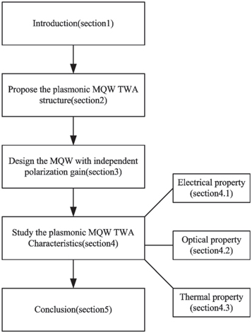
In this paper, firstly we propose the gap plasmonic MQW TWA structure and analyze the advantages of this structure in section 2. In section 3 we design the strain MQW for the independent polarization gain. In section 4 we simulate and analyze the gap plasmonic MQW TWA characteristics including the electrical, optical and thermal properties. Furthermore this paper flow chart is shown in figure A1 in the appendix.
2. The plasmonic TWA structure
The plasmonic MQW TWA structure is shown in figure 1(a). From top to down there are air cladding, noble metal Ag, SiO2 gap, MQW and semi-infinite InP substrate.
Figure 1. (a) the plasmonic MQW TWA cross-section; (b) the MQW structure.
Download figure:
Standard image High-resolution imageThe SiO2 gap width and height are  and
and  respectively. And the 100nm-height-Ag and MQW have the same width
  as SiO2 gap. The MQW is
  height.
On both sides of the MQW they are the p-InP and n-InP which guide current to pump MQW. This method is known as the lateral current injection(LCI). And the p-InP and n-InP doping concentration are  Both the positive and negative electrodes are
  width and
  from the MQW.
In figure 1(a), we adopt the hybrid gap plasmonic structure which is composed of noble metal Ag, low-index-gap (SiO2) and the high-index-MQW. The strong energy is confined in the SiO2 gap region for the continuity of the displacement field at the material interfaces, which leads to a strong normal electric-field component in the gap [11].
The reasons of using the MQW in our plasmonic TWA are as follows. Illustrated in figure 1(a) the MQW not only is the part of the above hybrid gap plasmonic structure, but also is the active medium to amplify the plasmonic wave. The plasmonic wave reaches its peak at the metal-dielectric-interface and decays quickly from both sides of this interface. For effectively amplifying the plasmonic wave, it is necessary to push the amplification medium close to the interface enough. By using the MQW pumped by lateral injection current, the quantum well (QW) can reach the metal-dielectric-interface very closely and amplify the plasmonic wave effectively.
Also in figure 1(a) the SiO2 is chosen as the gap material for three reasons. First, SiO2 is insulator, which isolates the metal Ag from the current injection areas. Second, the SiO2 has low refractive index, which is necessary in the hybrid gap plasmonic structure. Third, it is transparent in 1310 nm window which is the plasmonic TWA working range. In the above hybrid plasmonic structure, by adjusting the SiO2 gap height  and width
  the trade-off point between the mode field size and propagation loss can be moved to a suitable point.
3. The design of the MQW
Illustrated in figure 1(b), the MQW is consisted of 13 QW units, each of which includes the 5 nm-thickness-barrier, 9 nm-thickness-tensile-QW and 5nm-thickness-barrier from top to down. And these QWs are separated by the 30 nm separate confinement heterostructure (SCH) layers. Also shown in figure 1(b) at the top of the MQW it is the 5nm-thickness-InP which is next to the SiO2 gap area. Using the finite-element-method software COMSOL Mutiphysics, we find that the multi-guided-mode will appear if the whole MQW thickness is larger than  Therefore we use 13 QW units to compose the 612nm-thickness-MQW for single mode.
Research shows that in the QW the stimulated radiation light is composed of the TE and TM polarization waves [17]. These two polarization waves originate from the recombination of electron-heavy-hole and electron-light-hole separately. Generally in the QW structures the transition probability of the electron-heavy-hole is higher than that of the electron-light-hole, therefore the TE polarization wave is dominant. As a result the TE polarization gain is higher than the TM one in QW optical amplifier. So a number of designs have been developed to minimize the gain polarization difference in QWs, including alternation of tensile and compressive QWs [18], QWs with tensile barriers [19], low tensile strain QWs [20], tensile strained QWs with compressive barriers [21] and so on.
In this paper, for the polarization independent amplification we design the tensile-strain-QW. In this tensile-strain-QW, by increasing the tensile strain coefficient the bandgap of the light-hole is shrunk, which leads the TM polarization gain to rise and catch up with the TE one finally. Additionally, we use the  to realize all the layers of the MQW since it is known to have superior characteristics in temperature performance.
The design of the MQW includes several steps. In these steps the equation (1) [17, 22]and another finite-element-method software Crosslight PIC3D are used. Equation (1) is the relationship among the energy gap  the
the  ratio x,y and the strain coefficient. If the strain coefficient is given in equation (1), we can get that the x-y-equation and the relationship between
  and y. Furthermore, if
  also is given, the ratio x and y of the
  are determined. The MQW design flow chart is shown in figure 2.
Figure 2. The MQW design flow chart.
Download figure:
Standard image High-resolution imageBy these steps shown in figure 2, we get the  composition ratio
 ![$\left[x,y\right]$](https://content.cld.iop.org/journals/2631-8695/3/4/045029/revision2/erxac384aieqn19.gif) of the barrier, tensile-strain-QW and SCH layers to be
of the barrier, tensile-strain-QW and SCH layers to be ![$\left[0.203,0.267\right],\left[0.4198,0.0625\right]$](https://content.cld.iop.org/journals/2631-8695/3/4/045029/revision2/erxac384aieqn20.gif) and
and ![$\left[0.0646,0.4054\right].$](https://content.cld.iop.org/journals/2631-8695/3/4/045029/revision2/erxac384aieqn21.gif) The MQW energy band and QW material gain spectrum are also plotted as follows.
The MQW energy band and QW material gain spectrum are also plotted as follows.
By simulation, the MQW energy band structure is illustrated in figure 3(a) at 4v-bias-voltage. And in this figure, Ec, Evlh, Evhh, EFn EFp are the conduct band level, light-hole value band level, heavy-hole value band level, electron quasi Fermi level and hole quasi Fermi level separately. From this figure, it is shown the EFn>Ec in the QW regions when the MQW is applied 4v-bias-voltage, which indicates the carriers transition mainly occurs in these QW regions. In addition, shown in figure 3(a) inset the Evlh is higher than Evhh in the tensile-strain-QW, which leads to the TM polarization gain keeps pace with the TE one.
Figure 3. (a) the energy band structure of the MQW with 13 QWs at 4v-bias-voltage, inset one QW value band energy. (b)the QW material gain coefficients.
Download figure:
Standard image High-resolution imageIn figure 3(b) the QW material gain spectrums at different injected electron concentrations are listed. Three results can be available. First, the TE and TM polarization gains are close to each other in the 1310 nm wavelength window. Second, at 1317 nm wavelength the TE and TM gain peaks are approximately equal when the injected electron concentration ranges from  to
to  And this 1317 nm wavelength will be used at the following plasmonic TWA optical property simulation in section 4.2. Third, the QW material gain increases with the injected electron concentration rising.
In the above process, the QW material gains of the TE and TM polarization are calculated in equation (2) [23, 24] by the software Crosslight PIC3D.

of which the symbol explanations are listed in the table A1 in the appendix.
4. The plasmonic TWA characteristics
After getting the suitable layers component ratio and thickness of the MQW, we analyze the plasmonic TWA characteristics along the following steps.
First, in the section 4.1 we explore the MQW electrical properties by simulation and get the local gains of the MQW with different width  at different bias voltage
Second, in the section 4.2 we study the plasmonic TWA optical properties, explore this device gain threshold in different gap size, and find the suitable gap size at which this TWA has useful mode gain when the MQW is applied appropriate bias voltage.
Finally, in the section 4.3 the plasmonic TWA thermal property is analyzed on the condition of the different heat sources being considered.
In the above first and second steps, the MQW local gain is gotten in the MQW-InP dielectric waveguide structure in which the core is MQW, the substrate is InP, the n-InP and p-InP is on the both sides of the MQW and the cladding is air. And this MQW local gain is put into the plasmonic TWA for calculating the mode gain coefficient.
But the MQW local gain and mode field can interact with each other [24]. And this interaction is self-consistent. Therefore, theoretically only as the plasmonic TWA mode field in the MQW area is equal to that of the MQW-InP dielectric waveguide, the above processes are permissible.
In fact, in the plasmonic TWA the mode is a hybrid one between the plasmonic mode and that of the MQW-InP dielectric waveguide. When the MQW-InP dielectric waveguide mode is dominant, the above two steps can be acceptable.
Furthermore in the following section 4.2 we finally pick up the useful plasmonic TWA mode, in which the MQW waveguide wave is predominant indeed. Therefore the final results about this useful plasmonic TWA mode are reliable.
4.1. The MQW electrical property
The MQW simulation is based on the following equations [25]. These symbols' explanation and simulation parameters are shown in tables A1 and A2 in the appendix respectively.


The Poisson equation (3) and the carrier continuity equations (4) and (5) are used to get the electric potential  electron density n and hole density p. The optical rate equations (6) and (7) are utilized to calculate the photon density
  and
and  when the
  and
and  are known. The
  can be got by solving the Helmhertz equation (8). And the
  can be gotten from equation (2) using the n and p under the Lorentzian broadening condition in which the time constant is used and shown in table A2.
All of these equations are self-consistent and solved by circular iteration as the MQW bias voltage increasing. The software Crosslight PIC3D is used in this simulation.
In the above solution process the Auger recombination, spontaneous radiation recombination and SRH recombination must be considered. In other words, 

 need to be calculated using formulas from the published works as follows.
As for Auger recombination rate  the formula
  [23] is used, where
  are the electron, hole and intrinsic electron density respectively. And the Auger coefficients
  are assumed to be represented by the temperature dependent function
 ![$C\left(T\right)={C}_{0}\left({T}_{0}\right)exp\left[\displaystyle \frac{{E}_{A}}{k}\left(\displaystyle \frac{1}{{T}_{0}}-\displaystyle \frac{1}{T}\right)\right]$](https://content.cld.iop.org/journals/2631-8695/3/4/045029/revision2/erxac384aieqn40.gif) [26] where k is the Boltzmann constant,
[26] where k is the Boltzmann constant,  at
at  and
and  Utilizing these formulae the Auger coefficients in the QW, barrier and SCH regions at
  are gotten and shown in table A2.
The spontaneous radiation recombination rate  is calculated according to
  [27] where n is the electron density and B is the spontaneous radiation recombination coefficient also shown in table A2.
As to  there are two cases. One is the bulk recombination and the other is the surface recombination.
The bulk recombination in the QW, barrier, SCH, n-InP and p-InP area is described by the electrons and holes life time ( and
and  shown in the table A2) and it is assumed that a uniform distribution of donor mid-gap traps density is
  In the semi-insulation (SI) Fe-doped InP substrate and cladding, the bulk recombination is presented by the trap density
  electron and hole capture cross-section
  and the deep trap
  level below the conduction band edge which are taken from [28] and also listed in the table A2.
The surface recombination mainly originates from the poor quality of the vertical interfaces between the MQW region and the n-InP, p-InP area. This recombination can be described by the surface recombination velocity on these two vertical interfaces [29], of which parameter is in table A2, too.
And the intervalence-band absorption (IVBA) loss  is calculated from this formula
  in these quantum wells, barriers, SCH and bulk layer regions, where
  is the coefficient and p is the local hole density in table A2.
Apart from the above parameters, these default material parameters such as material refractive index, band gap, lattice constant, effective masses and carrier mobility are defined in the Crosslight PIC3D macrofiles for different regions.
By simulation two main results are discovered. The first one is that the MQW local gain and electron concentration rise up with the bias voltage  increasing. This conclusion is shown in figures 4(a)–(d). The 500nm-width-MQW local gains and electron concentrations at bias voltage
  are shown in figures 4(a) and (b) separately, in which along the vertical middle white dash line we get the different local gains and electron concentrations at
  shown in figures 4(c) and (d).

Figure 4. (a) and (b) are the MQW local gain and electron concentration as  and
and  (c) and (d) are the local gains and electron concentrations at different bias voltage
  along the middle vertical white dash line in (a) and (b) as
  (e) and (f) are the local gains and electron concentrations at different
  along the horizontal white dash line in (a) and (b) as
Download figure:
Standard image High-resolution imageThe second one is that at the fixed bias voltage the narrower the MQW width  the higher the MQW local gain and electron concentration illustrated in the figures 4(e) and (f). Along the horizontal white dash line in figures 4(a) and (b) the local gains and electron concentrations are shown in figures 4(e) and (f) at different
  at
at 
To describe the MQW electrical properties, we also explore the relationship between the bias voltage  injection current density and local gain as follows. Specifically in this plasmonic TWA the electrode width is
In figure 5(a) it shows the relationship curves between MQW injection current density and the bias voltage  at different
  From this figure two conclusions are gotten. The first one is that these injection current densities thicken with bias voltage
  increasing when
  is larger than the threshold voltage. Second, these MQWs with four different
  almost have the equal injection current densities at the same bias voltage
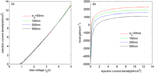
Figure 5. (a) the curves between the bias voltage  and injection current density about the MQW with different
  (b) the relationship between the injection current density and local gain at the center of the 7th QW at different
Download figure:
Standard image High-resolution imageIn figure 5(b) there are the curves about the total injection current density and the local gain at the center of the 7th QW which is the core of the MQW. Two points are discovered.
First, the local gains lift up with the injection current density rising. Specifically speaking, the local gains rise up dramatically with injection current density increasing as the injection current density is lower than  approximately. With the injection current density increasing further, the local gains reach saturation gradually, which is the well-known gain saturation in the optical amplifier [30].
Second is the local gain enlarges with  narrowing even as the injection current density is fixed. This phenomenon comes from the following reasons. When
  decreases, not only the internal quantum efficiency increases [31] but also the electron concentration thickens with
  dropping shown in figure 4(f). Therefore the local gain rises with
  narrowing, which is in agreement with that in figure 4(e).
From the above analysis, we can know that it is feasible to lift MQW local gain by increasing bias voltage  and narrowing MQW width
4.2. The TWA optical property
We first analyze the plasmonic TWA optical characteristics when the MQW has no applied voltage i.e. MQW has no local gain. And in the next step, we explore the MQW gain threshold in which the guided wave propagation loss is completely compensated. At last, by putting the MQW local gain into plasmonic TWA, we obtained the plasmonic TWA mode gains at different gap sizes.
Proven in section 3, at 1317 nm wavelength the MQW local gain is independent polarization, which is necessary to the plasmonic TWA. Therefore we simulate and analyze the plasmonic TWA optical properties at this wavelength.
In the following simulation the dielectric constants of these media in the plasmonic TWA are gotten as follows. The  dielectric constants
  are calculated from equation (9) [17].

where  are the InAs, GaAs and AlAs dielectric constants from the data in the [32]. All of these dielectric constants including the metal Ag, gap SiO2 and InP are calculated and shown in table A3 in the appendix.
Under the condition of MQW local gain being zero, we get the relationship curves between the gap size and plasmonic wave characteristics including the mode effective refractive index  mode attenuation coefficient and mode width. And the simulation is carried out by the software COMSOL Multiphysics
The definitions of the mode attenuation coefficient and mode width are explained as follows. If after propagating distance z (cm) the mode power is weakened by  the mode attenuation coefficient is defined as
  [30]. Also it is proposed the mode width describes the mode field lateral distribution which is important in the high integration density PIC. The mode width is defined as
  in the x direction, if
where the x and y represent the horizontal and vertical axis, the plasmonic TWA cross-section is y-axial symmetric.  is the plasmonic wave Poynting vector and the ratio of the mode power is
  assumed to be 50% in this paper.
By simulation several valuable results are explicit in figure 6. First, illustrated in figure 6(a) the guided mode has cut-off width of  If
If  is less than the cut-off width, the guided mode will not available. In detail, the guided mode effective index
  falls down with
  narrowed at fixed
  Until
Until  falls to 3.20 which is the lateral p-InP, n-InP and substrate InP refractive index, the guided mode will disappear.
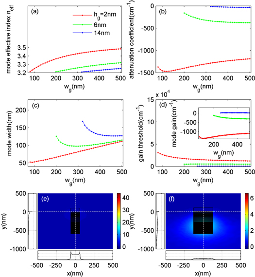
Figure 6. The mode properties of the plasmonic TWA at different gap width  and height
  (a) mode effective index
  (b) mode attenuation coefficient. (c) mode width. (d) the MQW local gain threshold for compensating mode loss completely, inset is the mode gain when the 4v-bias-voltage is applied to the MQW. (e) and (f) Poynting vector magnitude (unit:
 ) distribution for
 ![$\left[{h}_{g},{w}_{g}\right]=\left[2,90\right]{\rm{n}}{\rm{m}}$](https://content.cld.iop.org/journals/2631-8695/3/4/045029/revision2/erxac384aieqn106.gif) (e);
(e); ![$\left[{h}_{g},{w}_{g}\right]=\left[14,240\right]{\rm{n}}{\rm{m}}$](https://content.cld.iop.org/journals/2631-8695/3/4/045029/revision2/erxac384aieqn107.gif) (f). The magnitude of the Poynting vector along the vertical and horizontal white dashed lines across the middle of the gap is shown in the left and bottom boxes, respectively.
(f). The magnitude of the Poynting vector along the vertical and horizontal white dashed lines across the middle of the gap is shown in the left and bottom boxes, respectively.
Download figure:
Standard image High-resolution imageSecond the mode propagation loss decreases with the gap height  increasing, which is illustrated by the mode attenuation coefficient in figure 6(b). Therefore the mode propagation attenuation can be cut down by increasing the gap height
Third, the trade-off between the mode field size and mode propagation loss still exists. Indicated in figures 6(b), (c), as the  is thickened, the mode attenuation decreases and the mode width broadens. Therefore, the reduction of the mode propagation loss is accompanied by the mode field size extending when the
  is heightened.
Fourth, the guided mode is a hybrid one from the dielectric waveguide guided wave and plasmonic one. Depicted in figures 6(b), (c), at  both the mode attenuation coefficient and mode width have a minimum with
  variation from the following illustrations. In fact, the guide mode is affected by two actions. One comes from the plasmonic wave. The other one originates from the MQW-InP dielectric waveguide. If the plasmonic one is dominant, the mode width narrows and mode attenuation increases with
  diminishing. On the other hand, if the MQW dielectric waveguide action is superior, the mode width widens and mode attenuation lowers with
  falling down. Therefore the minimums mode width and maximum mode attenuation coefficient appear at the junction point of these two actions. As
  the minimum mode width appears at
  and the corresponding mode field is made clear in figure 6(f).
In the above simulation, it is assumed that MQW has no local gain. In the next part, we will explore the plasmonic TWA properties as MQW has local gain.
For getting the plasmonic TAW gain characteristics, we explore gain threshold and the mode gain. The gain threshold is the MQW local gain at which the plasmonic guided wave propagation loss is completely compensated in the plasmonic TWA. And the mode gain is the plasmonic TWA mode gain when the MQW is applied bias voltage. Here the applied bias voltage is 4 v.
By simulation we get the gain threshold shown in figure 6(d). Some results can be obtained from figure 6(d). First, the gain threshold rises up with  decreasing, which comes from the mode attenuation increasing with
  lowering in figure 6(b). Second, as
  the gain threshold goes up with
  narrowing for two reasons. One is the amplification area, i.e. the MQW area, shrinks with
  lowering. The other one is that the overlap between the mode field and MQW decreases as
  falling down.
The plasmonic TWA mode gain at 4v-bias-voltage is shown in figure 6(b) inset. This simulation result suggests several conclusions in the following. First, the plasmonic TWA mode gain can be risen up by thickening the  because the mode attenuation decreases with
  heightened. Second, it suggests that as
 ![$\left[{h}_{g},{w}_{g}\right]=\left[10,240\right]{\rm{n}}{\rm{m}}$](https://content.cld.iop.org/journals/2631-8695/3/4/045029/revision2/erxac384aieqn126.gif) and 4v-bias-voltage, the injection current density is
and 4v-bias-voltage, the injection current density is  the mode gain is
  and the mode width is 161 nm.
As ![$\left[{h}_{g},{w}_{g}\right]=\left[10,240\right]{\rm{n}}{\rm{m}},$](https://content.cld.iop.org/journals/2631-8695/3/4/045029/revision2/erxac384aieqn129.gif) the MQW-InP dielectric waveguide action is dominant in the plasmonic TWA described in figure 6(f). Therefore it is reasonable that in the MQW area the plasmonic TWA mode field is equal to the one in the MQW-InP dielectric waveguide approximately. And this result is utilized to explain this simulation results' reliability at the beginning of the section 4.
the MQW-InP dielectric waveguide action is dominant in the plasmonic TWA described in figure 6(f). Therefore it is reasonable that in the MQW area the plasmonic TWA mode field is equal to the one in the MQW-InP dielectric waveguide approximately. And this result is utilized to explain this simulation results' reliability at the beginning of the section 4.
4.3. The TWA thermal property
The thermal property is very important for semiconductor device. Therefore we explore the plasmonic TWA thermal characteristics with the same method as the [33].
Conservation of energy requires that the temperature distribution satisfies the equation (11).

where  is the density (kg m−3);
  is the specific heat capacity at constant pressure
 is the absolute temperature
 is the thermal conductivity
  Q is the heat sources density (W m−3).
For solving the equation (11), it is necessary to find out all the heat sources. In our plasmonic TWA the heat source can be separated into contributions from Joule heat, plasmonic wave decay heat and Auger recombination heat in the following.
The Joule heat is generated when the low frequency electrical current flows in the lossy material including the electrode, n-InP, p-InP and MQW. And the Joule heat power density can be calculated as  where
where  is the electrical conductivity and
  is the electric field.
The plasmonic wave decay heat comes from the attenuation while plasmonic wave is passing along the metal-semiconductor-interface. Since the SiO2 and InP are almost lossless in 1310 nm wavelength window, only the heat from the metal Ag is calculated. This heat source density is  where
where  is the optical frequency;
  is the imaginary part of the Ag permittivity.
  is the plasmonic wave electric field.
Auger recombination heat is defined as the energy heat emitted from the electron-hole pairs non-radiative recombination. The Auger recombination heat is given by  where
where  is the band gap energy of QW,
  and
and  are the Auger recombination coefficients, n and p are the electron and hole densities in QW respectively.
In our thermal simulation, there are some preconditions which are the bias voltage  the
the ![$\left[{h}_{g},{w}_{g}\right]=\left[10,240\right]{\rm{n}}{\rm{m}},$](https://content.cld.iop.org/journals/2631-8695/3/4/045029/revision2/erxac384aieqn149.gif) the
the  -height-substrate-InP,
  -thickness-cladding-air and the
  -width-simulation-zone. And the aluminum electrodes temperature is 300k since electrodes can be connected with heat sink. And the initial temperature of the system was 300 K.
The heat flux (or Neumman) condition is applied to the up and down boundaries with the external bulk temperature 300 K, while the Dirichlet condition is applied in the left and right boundaries also with temperature 300 K.
The simulations use literature values for the density, thermal conductivity, heat capacity of Ag, electrode Al, SiO2, InP, InAs, GaAs, AlAs [34, 35]. And those of the  are obtained by interpolation. The thermal simulation is also supported by these two software Crosslight PIC3D and COMSOL Multiphysics.
The plasmonic TWA thermal characteristics are deployed in figure 7. The whole thermal temperature of our plasmonic TWA is shown in figure 7(a) at  and
and ![$\left[{h}_{g},{w}_{g}\right]=\left[10,240\right]{\rm{n}}{\rm{m}}.$](https://content.cld.iop.org/journals/2631-8695/3/4/045029/revision2/erxac384aieqn155.gif) For more clear illustration, the central enlarged part is described in figure 7(b), which shows that the metal Ag and MQW are the highest temperature core. And we draw the temperature curves along the middle line of the device as guided wave power
For more clear illustration, the central enlarged part is described in figure 7(b), which shows that the metal Ag and MQW are the highest temperature core. And we draw the temperature curves along the middle line of the device as guided wave power  in figure 7(c). Also from figure 7(c), it is known that the plasmonic TWA core temperature rises up with the guided wave power
  increasing. Since the
  MQW has excellent performance from
  to
to  [36] and our plasmonic TWA temperature peak is less than 346 K
  as
as  shown in figure 7(c), this device can work well when

Figure 7. (a) the thermal temperature of the plasmonic TWA at  100nw guided wave power and
 ![$\left[{h}_{g},{w}_{g}\right]=\left[10,240\right]{\rm{n}}{\rm{m}}.$](https://content.cld.iop.org/journals/2631-8695/3/4/045029/revision2/erxac384aieqn165.gif) (b) the central part enlarged from (a). (c) the temperature along the vertical black dash line in the middle of the plasmonic TWA shown in the above (b) while the guided wave power
(b) the central part enlarged from (a). (c) the temperature along the vertical black dash line in the middle of the plasmonic TWA shown in the above (b) while the guided wave power  is 100nw,
  and
and  respectively.
Download figure:
Standard image High-resolution image5. Conclusion
We propose a deep-sub-wavelength scale plasmonic TWA with MQW. In our device the InGaAlAs tensile MQW is designed for the polarization-independent amplification. Simulation suggests that at 1317 nm wavelength the MQW gain is completely polarization independent. At this wavelength the mode width 161 nm and mode gain  can be reached in the condition of 10 nm × 240 nm gap size and 9.39 kA cm−2 injection current. And last but not least, when the plasmonic guided wave power is less than
  this plasmonic TWA has favorable thermal performance.
Acknowledgments
This work was supported by National Natural Science Foundation of China (Grant No.61605247) and the National University of Defense Technology Foundation (Grant No.ZK17-03-26).
Data availability statement
The data generated and/or analysed during the current study are not publicly available for legal/ethical reasons but are available from the corresponding author on reasonable request.
Appendix
Paper flow chart
Figure A1. This paper structure flow chart.
Download figure:
Standard image High-resolution image
Our paper is written according the flow chart.
Table A1. Equation symbols and their explanation.
| Symbol | Explanation |
|---|---|

| electron charge |

| bulk momentum transition matrix element. |

| photon energy |

| free space permittivity |

| electron mass |

| light speed in vacuum |

| material refractive index |

| thickness of the quantum well |

| conduction and valence band quantum numbers |

| spatially weighted reduced mass for transition |

| spatial overlap factor between the state  and and 
|

| angular anisotropy factor |

| electron quasi-Fermi functions in the conduction band |

| electron quasi-Fermi functions in the valence band |

| Lorentzian lineshape function |

| relative permittivity at direct-current. |

| electricstatic potential |
| p and n | mobile hole and electron density |
 and and 
| immobile ionized donor and acceptor density |

| electron and hole mobilities |

| electron and hole diffusion constants |

| Schokley-Read-Hall (SRH) recombination rate |

| Auger recombination rate |

| spontaneous radiation recombination rate |

| stimulated recommbination rate |

| photon density |

| photon live time |

| coupling coefficient of the spontaneous emitted power into optical mode |

| wave group velocity |

| local gain |

| wavelength in free space |

| wave number 
|

| permittivity at optical frequency |

| transverse optical modal shape |

| mode effective refrective index |
Table A2. Parameters in the MQW simulation.
| Parameter | Value | References |
|---|---|---|
Lorentzian time constant, 
| 0.1 ps | Crosslight PIC3D |
The Auger recombination coefficient in QW, barrier and SCH regions, 
|

| [26] |
| The spontaneous radiation recombination coefficient B in QW, barrier and SCH region |

| [27] |
The electron and hole lifetime in QW, barrier and SCH region, 
|

| Crosslight PIC3D |
The electron and hole lifetime in n-InP and p-InP region, 
|

| Crosslight PIC3D |
| Donor mid-gap traps density |

| Crosslight PIC3D |
| The trap density Nt of the substrate and cladding InP region |

| [28] |
Electron capture cross-section, 
|

| [28] |
Hole capture cross-section, 
|

| [28] |
Trap level below conduction band, 
| 0.63ev | [28] |
| The surface recombination velocity |

| [29] |
The intervalence-band absorption coefficient  of the barrier, SCH and bulk layer region of the barrier, SCH and bulk layer region |

| [26] |
The intervalence-band absorption coefficient  of the QW of the QW |

| [26] |
| Device temperature, T | 300k |
Table A3. Material dielectric constant at 1317 nm wavelength.
| Material | Dielectric constant |
|---|---|
| MQW barrier | 11.2181 |
| MQW SCH | 11.8544 |
| Tensile-QW | 11.8398 |
| Metal Ag | −67.3544–6.3369i |
| SiO2 | 2.3409 |
| InP | 10.2674 |