
Abstract
Thin-film solar cells are preferable for their cost-effective nature, least use of material, and an optimistic trend in the rise of efficiency. This paper presents a holistic review regarding 3 major types of thin-film solar cells including cadmium telluride (CdTe), copper indium gallium selenide (CIGS), and amorphous silicon (α-Si) from their inception to the best laboratory-developed module. The remarkable evolution, cell configuration, limitations, cell performance, and global market share of each technology are discussed. The reliability, availability of cell materials, and comparison of different properties are equally explored for the corresponding technologies. The emerging solar cell technologies holding some key factors and solutions for future development are also mentioned. The summarized part of this comparative study is targeted to help the readers to decipher possible research scopes considering proper applications and productions of solar cells.
Export citation and abstract BibTeX RIS
1. Introduction
In our solar system, the Sun is the most powerful light source that also happens to be the most accessible and inexpensive source of energy. The generated energy from solar does not produce any harmful emission thus reduces carbon dioxide (CO2) generation, which is one of the greatest advantages of using solar energy. It is also found that energy used by humans in a year is proportional to the Sunlight striking the Earth for an hour [1]. The photovoltaic (PV) transformation of sunlight into power is the most reliable system to fulfill future energy demand. This technology can also provide an effective solution to the mass destruction of nature.
The solar cell is a photovoltaic device—typically consisting of specifically prepared Silicon (Si) layers. The design of solar cells functions for the conversion of photons into electricity. The sunlight, consisting photons have enough energy to galvanize electrons in a semiconductor device to travel from lower to higher energy level creating electron-hole pairs. Generally, the electron flow from one to another layer of a junction by photoelectric effect creates a voltage difference and provides energy to another circuit. The amount of electricity created in a cell depends on some factors such as the size of the cell, quality of the light source, and materials used for creating the device.
It has been a while that crystalline silicon (c-Si) showed its value in the market with advantages including high performance (∼26.7%), ease of fabrication, and environmentally friendly traits [2]. Longevity is also a considerable advantage because c-Si modules deployed in the 1970s are still operating. Additionally, single-crystal panels can withstand the rough conditions accustomed to space travel [3]. Ironically, c-Si happens to be a poor light absorber along with an inflexible and fairly fragile when in an unordered amorphous structure. These solar cells are specifically used at places of high-performance requirements. The primary dissimilarity between thin-film and c-Si solar cells lies in the flexible pairing of PV materials. Thin-film solar cells are cheaper than mature c-Si wafer cells (sheets). Moreover, thin films are easier to handle and more flexible. They are also less vulnerable to destruction than their Si competitors. Although thin-film solar materials have slightly lower efficiency (η), they can outweigh the cost-benefit considering various applications.
To mitigate the issues regarding solar cell materials, several research groups collaborated on intensive experimental works. There are different types of separate works of literature available on the advances of solar cells regarding amorphous silicon (α-Si) [4], copper indium gallium selenide (CIGS) [5], and cadmium telluride (CdTe) [6]. Though some review papers reported several prominent technologies such as Lee and Ebong [2] and Kowsar et al [7], a single report consisting of all the aspects (efficiencies, developments, structure, specifications, and limitations) is not available. For this reason, a compact, well-organized, and informative paper with distinctive categories among the classifications will be highly beneficial for the best reading ability. As such, this paper delivers an outline of each state-of-the-art technology with all the features stated above on 3 primary kinds of thin-film solar cells.
In this document, we briefly reviewed thin-film solar cell technologies including α-Si, CIGS, and CdTe, commencing with the gradual development of the corresponding technologies along with their structural parameters and issues in section 2, which was then followed by the commercial module distribution of thin-film solar cells in comparison to c-Si in section 3. In section 4, we compared the devices' properties followed by section 5 that highlighted the next-generation technologies such as a dye-sensitized solar cell (DSSC), perovskite solar cell (PSC), organic solar cell (OSC), and quantum dot solar cell (QDSC). In section 6 we finalized and emphasized the noticeable achievements based on the analysis.
2. Thin film photovoltaics
Thin-film solar cell (TFSC) is a 2nd generation technology, made by employing single or multiple thin layers of PV elements on a glass, plastic, or metal substrate. The thickness of the film can vary from several nanometers to tens of micrometers, which is noticeably thinner than its opponent, the traditional 1st generation c-Si solar cell (∼200 μm thick wafers). This is why thin-film solar cells are amenable, lower in mass, and have limited resistance or abrasion [8–10].
2.1. Amorphous silicon solar cell
In the beginning, the α-Si solar cell used to be deposited in p-i-n structure but the device is likewise to be fabricated as an n-i-p formation sequence as well [7]; the historical progressions of α-Si solar cells are recapitulated in figure 1 and table 1 below.

Figure 1. Laboratory efficiencies of the α-Si solar cell.
Download figure:
Standard image High-resolution imageTable 1. Sequential developments of α-Si solar cell.
| Year | Applied methodology | Reported efficiency | Developed by |
|---|---|---|---|
| 1976–1977 | The 1st hydrogenated-α-Si (α-Si:H) solar cell was developed in a p-i-n formation employing doping gases while discharging. | 2.4% (S) | Carlson and Wronski at RCA Laboratories [11, 12] |
| Using Schottky barrier formation with 1.1 eV barrier heights for platinum (Pt) cells, close-ideal diode behavior was acquired. | 4% (S) | ||
| 1978 | Combined Schottky barrier formation with an insulating layer in metal-to-semiconductor (M–I–S) junction. The insulation layer was adjusted to equilibrate the low work function of inexpensive metal (nickel). | 4.8% (S) | Wilson and McGill at Heriot-Watt University, UK [13] |
| 1980 | The p-i-n formation with a 1.19 cm2 area was fabricated to decrease the loss characterizations. | 6.1% (S) | Carlson at RCA Laboratories [14] |
| 1981–1982 | Hydrogenated-amorphous silicon carbide (α-SiC:H) was produced by [SiH4(1−X)+CH4(X)] plasma decomposition with diborane (B2H6) or phosphine (PH3) dopant gas. The α-SiC:H/α-Si:H heterojunction device was created with 887 mV open-circuit voltage (Voc), 12.33 mA cm−2 short-circuit current (Jsc), and 0.653 fill-factor (FF). The fabricated structure became more successful with Voc = 880 mV, Jsc = 15.21 mA cm−2, and FF = 0.601. | 7.14% (S) 8.04% (S) | Tawada et al at Osaka University, Japan [15, 16] |
| 1986 | The insertion of a thin-film at the p-i interface affected short wavelength and performance with FF (0.771). | 8.43% (S) | Arya et al at Solarex Corporation, USA [17] |
| 1986 | Glass substrate without anti-reflection coating (ARC) resulted Voc = 12670 mV, Jsc = 78.47 mA cm−2, and FF = 0.667. | 9.63% (S) | Yamazaki et al at SEL [18] |
| 1992 | The double‐junction with the dual‐bandgap device was fabricated employing an appropriate deposition method. | 11% (M) | Guha et al at USSC [19] |
| 1996–1997 | A dual-junction structure of α-Si:H/α-Si:Ge with the decreased bandgap-alloyed device. Employed α-Si-based alloy in spectrum-splitting, triple-junction formation. Improved amorphous silicon germanium (α-SiGe) alloy, p-n tunnel junction, and top conducting oxide (TCO). | 11.8% (M) 13% (M) | Yang et al at USSC [20, 21] |
| 2013 | Developed a triple-junction device using α-Si:H/μc-Si:H/μc-Si:H formation. | 13.4% (M) | Kim et al at LGEARI [22] |
| 2015–2016 | By diode and triode plasma-enhanced chemical vapor deposition (PECVD), α-Si:H was fabricated at different rates. Decreasing deposition rates slightly lowered light-induced degradation. Decreased metastable defect and increased bandgap were attributed to deposition rates (1–3 × 10⁻² nm s−1) and triode PECVD. | 10.22% (S) | Matsui and Sai at AIST [23–25] |
| Similarly α-Si:H/μc-Si:H tandem device was produced. | 12.69% (M) | ||
| Higher Jsc (32.9 mA cm−2) was acquired from a periodically textured substrate and incorporated for a triple-junction. | 13.6% (M) | ||
| After equalizing Jsc and FF, light-induced degradation was minimized (4%). | 14.04% (M) |
S: single-junction; M: multi-junction (micromorph)RCA: Radio Corporation of America, USA; SEL: Semiconductor Energy Laboratory, Japan; USSC: United Solar System Corporation, USA; LGEARI: LG Electronics Advanced Research Institute, Korea; AIST: National Institute for Advanced Industrial Science & Technology, Japan
2.1.1. Structure of a-Si
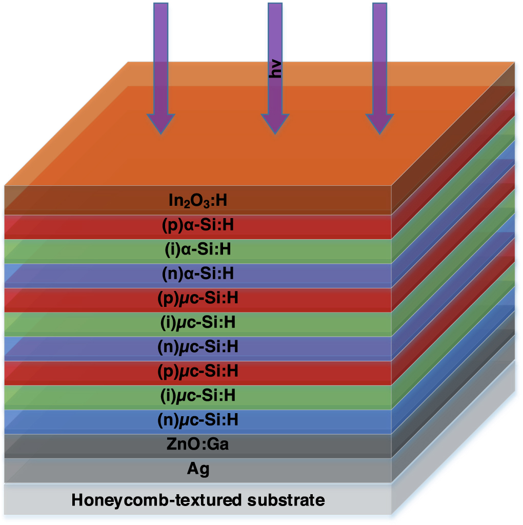
This solar cell with a random crystal structure is usually developed on a fluorine (F)-doped tin oxide (SnO2:F) fabricated glass substrate for single-junction or periodically (honeycomb)-textured substrate (HTS) for micromorph (tandem) structure. To reduce reflective loss and increase conductivity, normally silver (Ag) and gallium (Ga)-doped zinc oxide (ZnO:Ga) coatings are applied on the substrate, successively. Then hydrogenated-α-Si (α-Si:H) is generally deposited by a diode or triode plasma-enhanced chemical vapor deposition (PECVD) employing CO2, phosphine (PH3), diborane (B2H6), silane (SiH4), and hydrogen (H2) dopant gases. After this process, transparent conducting oxide (TCO) film as the front window is deposited typically of indium tin oxide (In2O3:Sn) or hydrogenated-indium oxide (In2O3:H) (IOH) by radio frequency (RF) magnetron sputtering. As the grid electrode, Ag can be deployed, following which, a moth-eye-based anti-reflection coating (ARC) can also be applied to improve cell performance [25].
In the latest technology, the single-junction [SLG/Ag/GZO/(n)α-Si:H/(i)α-Si:H(diode/triode)/(p)α-Si:H/ITO/Ag] device was fabricated by diode PECVD, where the tandem (triple-junction) [HTS/Ag/GZO/μc-Si:H/μc-Si:H/a-Si:H(diode/triode)/IOH/Ag] device was fabricated by triode PECVD. For the triple-junction module, reactive ion etching was used for isolating the cells along with nano-crystalline silicon oxide (nc-SiOx) layers. The device was arranged with a hydrogenated-micro-crystalline Si (μc-Si:H) as the bottom (∼1.8 μm thick), a μc-Si:H as the middle (∼1.6 μm thick), and a α-Si:H as the top (∼230 nm thick) cell. Each of the μc-Si:H cells were stacked as the given substrate type arrangement: (n)μc-Si:H/(n)nc-SiOX/(i)μc-Si:H/(p)nc-SiOX/(p)μc-Si:H [25]. Figure 2 demonstrates the state-of-the-art layout of a triple-junction n-p α-Si:H/μc-Si:H/μc-Si:H solar cell.

Figure 2. The layout of a triple-junction n-p α-Si:H/μc-Si:H/μc-Si:H solar cell was adapted from [25].
Download figure:
Standard image High-resolution image2.1.2. Specifications of a-Si
Table 2 displays the latest α-Si solar cell parameters.
Table 2. Latest α-Si solar cell parameters [25].
| Year | Area (cm2) | Voc (mV) | Jsc (mA/cm2) | FF (dec) | η (%) | Test center |
|---|---|---|---|---|---|---|
| 2016 | 1.05 | 1922 | 9.94 | 0.734 | 14.04 | AIST |
2.1.3. Limitations of a-Si
Our identified critical issues regarding α-Si solar cells are:
- 1.The deposition process requires improvement that is important for the large-scale manufacturing of this solar cell [26].
- 2.Light scattering properties have to be dealt with by improving the optoelectronic properties of the front TCO component [27].
- 3.Staebler-Wronski effect needs to be resolved by finding a suitable way to impede the light-induced degradation of the device structure [28].
In the case of the α-Si:H solar cell, due to the creation of an electron-hole pair by an absorbed photon in the intrinsic layer, the electric field induced across the intrinsic layer causes electrons to drift to n-layer and holes to p-layer. A thin graded interface layer is usually employed to reduce the p/i interface defects—responsible for low open-circuit voltage (Voc) and short-circuit current (Jsc), to improve cell performance.
2.2. Copper indium gallium selenide solar cell
In the beginning, the CIGS solar cell was a plain p-CuInSe2/n-CdS heterojunction [29] but the device structure has been configured towards substrate/Mo/CIGS/CdS/ZnO/AZO/Al formation mostly [30, 31]; the historical progressions of CIGS solar cells are recapitulated in figure 3 and table 3 below.
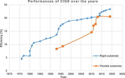
Figure 3. Laboratory efficiencies of the CIGS solar cell.
Download figure:
Standard image High-resolution imageTable 3. Sequential developments of CIGS solar cell.
| Year | Applied methodology | Reported efficiency | Developed by |
|---|---|---|---|
| 1976–1977 | The 1st CIGS solar cells were developed through 2 modes of 100 mW cm−2 tungsten-halogen illuminations for 1.2 cm2 (p-CuInSe2/n-CdS) devices. | 4.5% (R) | Kazmerski et al at University of Maine, USA [29, 32] |
| Heterojunction materials including ternary (CuInSe2, CuInS2, CuInTe2) and binary indium phosphide (InP) with cadmium sulfide (CdS) were fabricated by vacuum deposition. | 5.7% (R) | ||
| 1980–1982 | Polycrystalline CdS/CuInSe2 heterojunction device was produced by continuous material evaporation to deposit copper indium diselenide (CuInSe2) layer and showed an increased Jsc (31 mA/cm2) for 1 cm2 device. | 5.7% (R) | Mickelsen and Chen at Boeing Aerospace Company, USA [33–36] |
| The device was constructed by vacuum deposition and sputtering on cheap substrates. | 7.5% (R) | ||
| The Jsc was 35 mA cm−2 and the film thickness was 5 μm. | 9.5% (R) | ||
| Mixed ZnxCd1−xS used to enhance Voc. | 10.6% (R) | ||
| 1985 | Introduced zinc oxide (ZnO) combining p-CuInSe2 with thin undoped (Cu,Zn)S or CdS. The n-CdS film harvested photons with <520 nm wavelength and ZnO ARC enhanced Jsc by 25%. | 11.2% (R) | Potter et al at ARCO Solar Inc., USA [37] |
| 1988 | The ZnO/CdS/CIS cell was analyzed to find that tunneling and series resistance controlled low-temperature characteristics, where recombination limited cell efficiency. | 12.2% (R) | Mitchell and Liu at ARCO Solar Inc., USA [38] |
| 1990 | Polycrystalline ZnO/CdZnS/CuInGaSe2 device was fabricated through employing CuInGaSe2 by Physical Vapor Deposition (PVD), CdZnS by chemical vapor deposition (CVD), and ZnO by reactive sputtering. | 12.5% (R) | Devany et al at Boeing Aerospace and Electronics, USA [39] |
| 1993 | CuInGaSe2 was obtained by electron (E)-beam evaporated layers with hydrogen selenide (H2Se) gas reaction at 400°C, where molybdenum (MO), titanium (Ti), and aluminum (Al) were substrates. | 8.3% (F) | Başol et al at ISET [40] |
| 1993 | Polycrystalline CuIn(1−x)GaxSe2 device was made by material evaporation of selenide (Se), chemical deposition of cadmium zinc sulfide (CdZnS) (20–30 nm), and radio-frequency (RF) sputtering of transparent conducting oxide (TCO) ZnO layer. The gallium (Ga)-rich cell and reduced optical losses caused the improvement. | 13.7% (R) | Chen et al at Boeing Defense and Space Group, USA [41] |
| 1994–1995 | CuInxGa(1−x)Se2 was built from (Inx,Ga1−x)2Se3 precursor layers by co-evaporating indium (In), Ga, and Se. The cell was exposed to a flux of copper (Cu) and Se. | 15.9% (R) | Gabor and Tuttle et al at NREL [42, 43] |
| The integration of Ga in Cu(In,Ga)Se2 device increased the absorber layer bandgap, Voc (654 mV), and FF (>0.77). | 17.1% (R) | ||
| 1996 | Less temperature with the polymeric substrate was employed for depositing CdS window layer and ZnO. | 9.3% (F) | Başol et al at ISET [44] |
| 1996 | Grid design modifications were done, where the intrinsic ZnO (i-ZnO) layer was critical for developing the cell. | 17.7% (R) | Tuttle et al at NREL [45] |
| 1999 | With no buffer layer, a cadmium (Cd)-free cell was fabricated by PVD and direct ZnO deposition on Cu(In,Ga)Se2 layer. | 15% (R) | Contreras et al at NREL [46] |
| The ZnO/CdS/Cu(In,Ga)Se2/Mo polycrystalline cell led to further improvement. | 18.8% (R) | ||
| 2003 | Improved ZnO/CdS/CuInGaSe2 device was obtained due to more characterization. | 19.2% (R) | Ramanathan et al at NREL [47] |
| 2005 | Cu(In,Ga)Se2 device improvement was attributed to absorber bandgap (1.14 eV), decreased diode saturation current density (3 × 10⁻⁸ mA cm−2), diode quality (1.30<n<1.35), and lowered space-charge recombination. | 19.5% (R) | Contreras et al at NREL [48] |
| 2008 | Deposition recombination was reduced for process termination with Ga-poor (In-rich) film. | 19.9% (R) | Repins et al at NREL [49] |
| 2010 | Maximum efficiency gained using Mo flexible substrate by a 3-stage co-evaporation process. | 14.6% (F) | Niki et al at AIST [50] |
| 2010 | Recorded more improved Cu(In,Ga)Se2 thin cell. | 20.1% (R) 20.3% (R) | Jackson et al at ZSW [51] |
| 2011–2012 | Stainless-steel (SS) substrate temperature was reduced while depositing CIGS. | 17.1% (F) | Reinhard and Pianezzi et al at EMPA [52, 53] |
| Employing CIGS growth further enhanced performance. | 17.7% (F) | ||
| 2013 | The highest efficiency was gained for polymer foil substrate. | 20.4% (F) | EMPA and FhG-ISE [54] |
| 2013–2014 | Generated Cu(In,Ga)Se2 devices by static co-evaporation process and employing Zn(O,S) buffer layers. | 20.4% (R) | Powalla and Jackson et al at ZSW [55, 56] |
| Potassium (K)-doped film increased Ga material. | 20.8% (R) | ||
| 2014 | With high deposition rates and co-evaporation of the CIGS absorber film, the performance was improved. | 21% (R) | Herrmann et al at Solibro Hi-Tech GmbH, Germany [57] |
| 2014 | An improved efficiency was reported. | 21.7% (R) | Jackson et al at ZSW [58] |
| 2015 | The CIS absorber layer and junction creation were improved. | 22.3% (R) | Solar Frontier and ZSW [59] |
| 2016 | Employing alkali substances rubidium (Rb) and cesium (Cs) in alkali post-deposition treatment (PDT) actuated the alkali material process in the absorber and improved diode quality. | 22.6% (R) | Jackson et al at ZSW [60] |
| 2017 | Using alkali element Cs and modifying the absorber layer allowed a wider bandgap thus reverse saturation current density was improved. | 22.9% (R) | Wu et al at AIST [61] |
| 2019 | Using the roll-to-cell process, the device was fabricated on a SS foil substrate. | 20.56% (F) | Bayman et al at NREL [62] |
| 2019 | A Cd-free Zn(O,S,OH)x/Zn0.8Mg0.2O double-buffer layer Cu(In,Ga)(Se,S)2 device was generated by chemical bath deposition (CBD) and atomic layer deposition (ALD). | 23.35% (R) | Nakamura et al at AIST [63] |
R: rigid substrate; F: flexible substrate (polymeric).ISET: International Solar Electric Technology, USA; NREL: National Renewable Energy Laboratory, USA; ZSW: The Center for Solar Energy & Hydrogen Research, Germany; EMPA: Swiss Federal Laboratories for Materials Science & Technology, Switzerland; FhG-ISE: Fraunhofer Institute for Solar Energy Systems, Germany.
2.2.1. Structure of CIGS
This solar cell with a chalcopyrite crystal structure is usually developed on ultrasonically washed and dried rigid substrates; moreover, polymeric flexible substrates are also being used [64]. Molybdenum (Mo)-as a back contact as well as the reflector of most unabsorbed light, is normally sputtered on a soda-lime glass (SLG) substrate. The absorber layer, Cu(In,Ga)(Se,S)2 (∼2 μm thick) is created by physical vapor deposition (PVD) for sulfurization-after-selenization (SAS) of the precursor layers generally by hydrogen selenide (H2Se) gas that naturally gives rise to Mo(S,Se)x film between the absorber and back contact. At times, applied cesium (Cs) treatment thermally evaporated cesium fluoride (CsF) on the absorber layer, following which cadmium sulfide (CdS) (∼50 nm thick) or cadmium (Cd)-free buffer layer typically through chemical bath deposition (CBD) is placed on top [63]. Then an intrinsic zinc oxide (i-ZnO) (∼100 nm thick) layer covered by aluminum (Al)-doped ZnO (ZnO:Al) as TCO layer is fabricated on CdS buffer by chemical vapor deposition (CVD) to avoid external damage [65].
In the latest technology, a 2nd buffer layer of magnesium (Mg)-doped ZnO (ZnO:Mg) (∼50 nm thick) was fabricated by atomic layer deposition (ALD) on the 1st Cd-free Zn(O,S,OH)x (∼50 nm thick) buffer to enhance the cell performance. Whereas, Metal-organic CVD (MOCVD) was used to deposit the boron (B)-doped ZnO (ZnO:B) layer as TCO. After that Al and magnesium fluoride (MgF2) were evaporated through electron (E)-beam evaporation for producing the electrode and ARC, correspondingly. The ratio of Ga to (Ga+In) was around 0.3, where metal compositions like this were deposited with an additive such as sodium (Na) to form the precursor layers [63]. Figure 4 demonstrates the state-of-the-art layout of a rigid-substrate double-buffer CIGSSe solar cell.

Figure 4. The layout of a rigid-substrate double-buffer CIGSSe solar cell was adapted from [63].
Download figure:
Standard image High-resolution image2.2.2. Specifications of CIGS
Table 4 displays the latest CIGS solar cell parameters.
Table 4. Latest CIGS solar cell parameters [63].
| Year | Area (cm2) | Voc (mV) | Jsc (mA/cm2) | FF (dec) | η (%) | Test center |
|---|---|---|---|---|---|---|
| 2019 | 1.04 | 734 | 39.60 | 0.804 | 23.35 | AIST |
2.2.3. Limitations of CIGS
Our identified critical issues regarding CIGS solar cells are:
- 1.At lower temperatures, a feasible development of the deposition process onto a flexible substrate is required for this solar cell.
- 2.Although many substances for producing the device are earth-abundant, the metal indium (In) is scarce, which led to the searching for alternative materials.
- 3.The CdS layer deposited by CBD employs toxic Cd and thiourea (CH4N2S), producing wastage; additionally, selenide (Se) compounds like H2Se are extremely toxic that need minimization [66].
In the case of the CIGSSe solar cell, the ZnO:Al (AZO) layer is employed as TCO to gather and transfer electrons out of the cell when transmitting as much light as possible. For the negative impacts on ecology and limitation of resources, a search for less toxic substances gave birth to the CZTS solar cell formed of wholly earth-abundant elements.
2.3. Cadmium telluride solar cell
In the beginning, the CdTe solar cell was configured as a substrate formation but the structure was changed to a superstrate arrangement [67, 68]; the historical progressions of CdTe solar cells are recapitulated in figure 5 and table 5 below.

Figure 5. Laboratory efficiencies of the CdTe solar cell.
Download figure:
Standard image High-resolution imageTable 5. Sequential developments of CdTe solar cell.
| Year | Applied methodology | Reported efficiency | Developed by |
|---|---|---|---|
| 1972 | The 1st CdTe/CdS solar cell was developed by a thin-film graded gap and a 3-step process, including high-temperature vapor phase deposition (VPD) for p-CdTe and high vacuum evaporation for the n-CdS film. | 6% (B) | Bonnet & Rabenhorst [69] |
| 1976 | A ceramic thin-film (20 μm) was fabricated by a screen printing technique that showed a 0.2 Ω-cm resistivity. | 8.1% (P) | Nakayama et al at MEI [70] |
| 1982 | Introduced very thin polycrystalline CdS and CdTe semiconductor films, produced by closed-space sublimation (CSS) on soda-lime glass (SLG) coated with indium oxide (In2O3) that acted as a contact electrode. To secure shallow-junction behavior, oxygen (O) was induced. The obtained Voc = 750 mV, Jsc = 17 mA cm−2, and FF = 0.62. | 10.5% (P) | Tyan & Perez at Eastman Kodak Co. [71] |
| 1982 | ITO/CdTe and CdS/CdTe heterojunction devices were produced by E-beam evaporation of indium tin oxide (ITO) or CdS on p-CdTe. ITO/CdTe junction included air heat treatment. Surface treatment included etching by (110) and (111) bromine (Br)‐in‐methanol (CH3OH) and heating by hydrogen (H) were obtained. | 7.5% (P) | Werthen et al at Stanford University, USA [72] |
| With high tellurium (Te), etched surfaces have decreased effect in junction creation (Jsc = 20 mA cm−2). | 9% (P) | ||
| Low-doped CdTe gave Voc = 810 mV for high diode factor by changing recombination (interfacial-depletion). | 10.5% (P) | ||
| 1982 | Employed closed-spaced vapor transport deposition (VTD) to prepare p-CdTe on an n-CdTe substrate. Combination of n-element doping gradient, p-doped front film, and optimizing junction created a productive shallow p+nn+ form with Voc = 850 mV, Jsc = 20 mA cm−2, and FF = 0.7. | 11% (P) | Cohen et al at CNRS [73] |
| 1983–1984 | The high amount of O2 in the environment, carbon (C) electrode, and Cu-addition in C paste decreased series resistance and diode factor; resulting in Voc = 754 mV, Jsc = 22 mA cm−2, and FF = 0.606. | 12.8% (P) | Kuribayashi & Matsumoto et al at MEI [74, 75] |
| Employing a screen printing technique, the same efficiency was achieved for a 0.78 cm2 with a 2 mm thick device. | |||
| 1990 | A fabricated (Glass/ITO/CdS/CdTe/Cu-Au) device provided high Jsc (28 mA cm−2) and reduced bandgap. | 13.1% (P) | Morris et al at Queensland Univ., Australia [76] |
| 1991–1992 | A solution of Cd salt, ammonium (NH4) salt, and thiourea (CH4N2S) were used to prepare CdS. The CSS deposited p-CdTe and CdS were optimized through the temperature and composition of elements. | 13.4% (P) | Chu et al at University of South Florida, USA [77, 78] |
| The cell was deposited by fluorine (F)-doped SnO2, CdS, p-CdTe, and ohmic contact on a glass substrate through ARC. | 14.6% (P) | ||
| 1993 | CBD and CSS were applied to prepare the n-CdS buffer layer and deposit the p-CdTe absorber layer, respectively. The reported values were Voc = 843 mV, Jsc = 25.1 mA/cm2, and FF = 0.745. | 15.8% (P) | Britt & Ferekides at University of South Florida, USA [79] |
| 1997 | Metal-organic CVD was employed to deposit extremely thin CdS (50 nm) film on ITO, where CdTe was deposited by CSS to fabricate the cell on a glass substrate. | 16% (P) | Ohyama et al at MBI [80] |
| 2001 | A changed polycrystalline cell formation (CTO/ZTO/CdS/CdTe) led towards a high Jsc = 26 mA cm−2 and FF = 0.773. | 16.5% (P) | Wu et al at NREL [81] |
| 2006 | CdS/CdTe device was further analyzed for near-ideal bandgap (1.45 eV) and high absorption coefficient. | 16.5% (P) | Morales at IPN [82] |
| 17.3% (P) | |||
| 18.7% (P) | |||
| 2011–2016 | By the CSS method, the CdS/CdTe hetero-junction cell was developed on a glass substrate. The CdS window layer was fabricated by VTD following the deposition of the CdTe absorber layer. Further continuation of the research directed towards the highest efficient commercialized device. | 19.6% (P) | First Solar Inc. [83–88] |
| 20.4% (P) | |||
| 21% (P) | |||
| 22.1% (P) |
B: substrate; P: superstrate.MEI: Matsushita Electric Industrial Co. Ltd, Japan; CNRS: The French National Center for Scientific Research, France; MBI: Matsushita Battery Industrial Co. Ltd, Japan; IPN: National Polytechnic Institute, Mexico.
2.3.1. Structure of CdTe
This solar cell with a zinc (Zn) blend crystal structure is usually developed on ordinary glass substrates, preferably a heat-strengthened front SLG. Here, TCO is frequently a SnO2:F (FTO), In2O3:Sn (ITO), or cadmium tin oxide (Cd2SnO4)—behaves like the front contact and works as a window layer. The n-type CdS (∼100 nm thick) window layer, nowadays deployed as a buffer layer, can be deposited by CBD, sputtering, vacuum evaporation, etc [68, 89]. Then p-type CdTe (∼5 μm thick) absorber layer can also be deposited by PVD, sintering, screen-print, etc. The Al, Mo, gold (Au), nickel (Ni), or platinum (Pt) can be deployed as a back contact (metal contact) employing the vacuum thermal evaporation (VTE) technique [7].
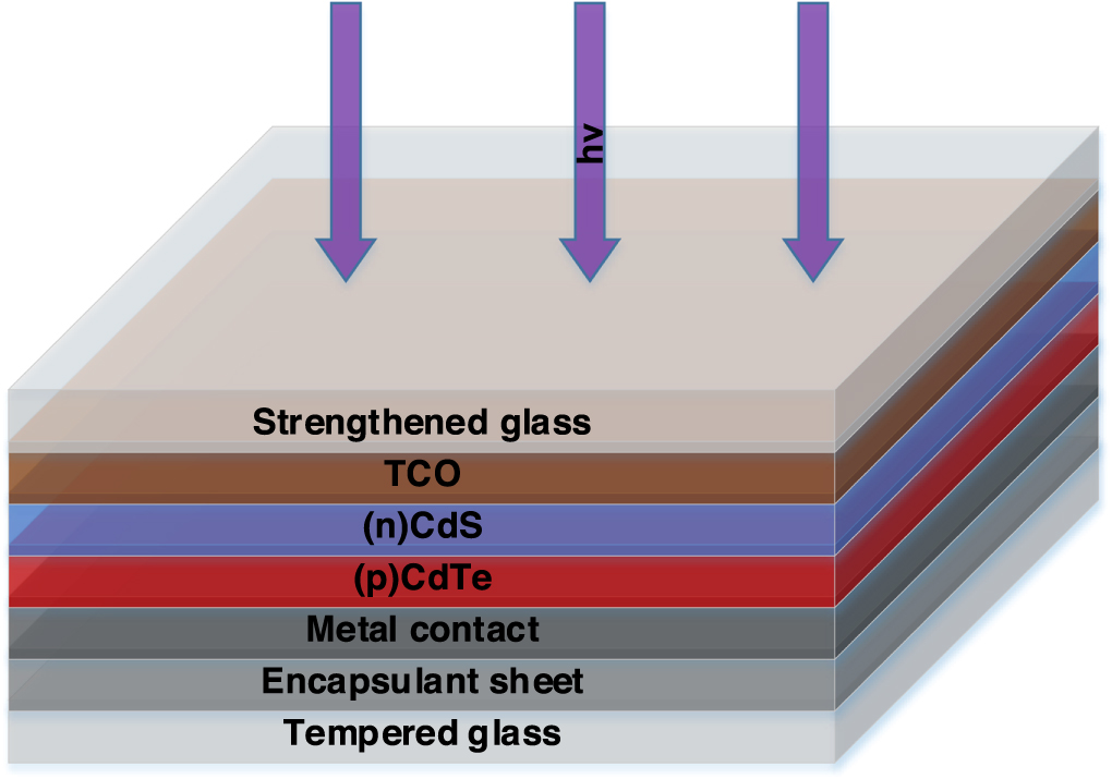
In the latest technology, the cell was laminated between 2 layers of glass, where the 2nd layer was normally a heat-tempered back SLG. Furthermore, a transparent encapsulate sheet—ideally ethylene vinyl acetate (EVA) (a polymeric adhesive) was used for the protection and sealing from delamination due to possible chemical degradation. After employing copper (Cu)-doped zinc telluride (ZnTe:Cu) metal contact, the CdTe film was fabricated by closed-space sublimation (CSS), followed by a cadmium chloride (CdCl2) treatment; whereas, the CdS film was fabricated by vapor transport deposition (VTD). The FTO as TCO was coated along with an optional buffer layer (SnO2, ZnO, ZnO:Mg) by MOCVD on the front glass [90–92]. Figure 6 demonstrates the state-of-the-art layout of a superstrate glass-glass CdTe/CdS solar cell.

Figure 6. The layout of a superstrate glass-glass CdTe/CdS solar cell was adapted from [2].
Download figure:
Standard image High-resolution image2.3.2. Specifications of CdTe
Table 6 displays the latest CdTe solar cell parameters.
Table 6. Latest CdTe solar cell parameters [93].
| Year | Area (cm2) | Voc (mV) | Jsc (mA/cm2) | FF (dec) | η (%) | Test center |
|---|---|---|---|---|---|---|
| 2016 | 0.48 | 887 | 31.69 | 0.785 | 22.10 | Newport |
2.3.3. Limitations of CdTe
Our identified critical issues regarding CdTe solar cells are:
- 1.The central danger during the active lifetime of this solar cell is dissolving out of broken modules and creating fire hazards, which need to be avoided.
- 2.As a by-product of Zn refining, abundant-element Cd is obtained; however, as a by-product of Cu refining, rare-element tellurium (Te) is obtained, creating material shortage [94].
- 3.One of the primary elements Cd is very toxic and known as a carcinogenic as well as environmentally hazardous material, though the produced PV compound has reduced toxicity and increased stability [95].
In the case of the CdTe/CdS solar cell, TCO primarily serves as front contact and lateral current-carrying conductor. The CdCl2 treatment extends grain size that considerably increases the overall conversion efficiency.
In terms of laboratory efficiency, the record performance for α-Si single-junction is 10.22% and the multi-junction is 14.04%. To date, the maximum performance of the CIGS rigid substrate is 23.35% and the flexible substrate is 20.56%. Whereas, 22.1% is the highest performance for superstrate CdTe solar cells.
A few mentionable thin-film photovoltaics are briefly described as follows.
2.4. Copper zinc tin sulfide solar cell
The copper zinc tin sulfide (CZTS) or Cu(Zn,Sn)(S,Se)2 is a 4th order semiconducting composite with a tunable bandgap along with the most common, kesterite crystal structure for PV applications. The cell shows interesting optical and electronic characteristics, close to CIGS. Thus this technology is continuously receiving increasing attention. With a similar fabrication technology as CIGS, this device employs elements like Zn and Sn instead of In and Ga [96–98]. The best cell was acquired by a combination of poor-Cu and rich Zn with a controlled bandgap through the S/Se ratio. Unlike CIGS or CdTe, it is produced from available and non-toxic materials [99] that makes it cheaper than CIGS. So, the major advantages of CZTS are the employment of inexpensive raw, abundant, and harmless materials [100]. However, this technology indicates a high voltage loss for the recombination at defects in the bulk device as well as charge extraction interfaces. Recent improvements for the module led to the achievement of increased efficiency of 12.6% in the lab environment [101]. Finding another rear contact, having less optical loss meaning higher reflectivity, can endure the operation of the device and keep a decreased series resistance to bring significant progress for the device [96].
2.5. Gallium arsenide solar cell
The gallium arsenide (GaAs) is an III-V direct bandgap semiconductor. It contains a Zn blend crystal formation and is often employed as a substrate for epitaxial growth of other III-V semiconducting devices. As a valuable semiconductor of high performance in a high-temperature environment, single and multi-crystalline thin-film photovoltaics are made by it and used in space. This hetero-structured device has higher electron mobility and saturated electron velocity, allowing GaAs-based transistors to operate at more than 250 GHz [102–104]. Because of having a wider energy bandgap, GaAs are good at resisting heat and creates less electrical signal disturbance in electronics than Si-devices—meaning it has higher carrier mobility. Being a direct bandgap material [105], GaAs-based solar cells can efficiently absorb and emit light. Additional benefits include low manufacturing cost, lightweight cells, and compact design that permits flexibility in installation [106]. Even though GaAs/Ge solar cells can cost 5–10 times higher than Si-based solar cells, the improved performance reduced the area and weight of the photovoltaic array. With a maximum performance for single-junction photovoltaics at 29.1%, GaAs with germanium (Ge) and indium gallium phosphide (InGaP)-layered triple-junction photovoltaics recorded efficiency of over 32% [107]. The highly efficient material is obtained due to the extremely high-quality epitaxial growth of GaAs, surface passivation by aluminum gallium arsenide (AlGaAs), and promotion of photon recycling by designing thin-film [102].
These solar cells are seeking attraction through their potential to high performance and balanced characteristics to ecology.
3. Commercial module distribution
The thin-films industries propelled in the market from 2001 to 2009 by increasing production from 14 MW to 2,141 MW through the involvement of over 100 companies [93].
Figure 7 represents the best laboratory-developed solar cells. It is observable that the highest performance is recorded 26.7% for mono-crystalline Si modules, where poly-crystalline Si has 23.2% efficiency at most. The recorded maximum efficiency for the α-Si solar cell is 14.04% (multi-junction), CIGS is 23.35% (rigid substrate), and CdTe is 22.1%. In the realm of thin-films, CIGS tops the laboratory-developed modules in terms of performance. Additionally, III-V semiconductors' research device of six-junction (AlGaInP/AlGaAs/GaAs/GaInAs) concentrator PV (CPV) technology reached the maximum (∼47%) efficiency [93].

Figure 7. Best laboratory-developed solar cells.
Download figure:
Standard image High-resolution imageFigure 8 depicts the champion commercially manufactured solar cells, indicating mono c-Si have the most efficient (24.4%) modules developed by Kaneka Corporation, Japan; whereas, the Hanwha Q Cells from Germany offer the maximum performed (20.4%) poly c-Si cells. The TEL Solar from Switzerland showed the most prominence 12.3% efficient α-Si multi-junction business modules. In the thin-films industry, CIGS rigid substrate has the greatest eminence with a 19.2% commercialized module from Solar Frontier, Japan. One of the reputable CdTe companies, First Solar Inc., USA is manufacturing devices with the highest 19% efficiency. To this date, the most efficient (∼40%) four-junction hybrid CPV module is being manufactured by the University of New South Wales (UNSW), Australia [108].

Figure 8. Champion commercially manufactured solar cells.
Download figure:
Standard image High-resolution imageFigures 9(a) and (b) illustrate the global PV production of 2010 and 2019, with 17.2 GW [109] and 121 GW [110] respectively, where the compound annual growth rate (CAGR) was 24.2%. The shipments of Si modules altogether increased from 87% (2010) to 95.5% (2019), separately increased for single-crystalline Si (38% to 63%) and decreased for multi-crystalline Si (49% to 32.5%). Even though thin-films modules indicated a progressive decline from 13% (2010) to 4.5% (2019), CdTe continuously held the highest portion of production with 8% and 2.3% accordingly. Simultaneously, CIGS (2% to 1.9%) and α-Si (3% to 0.3%) shipments lowered significantly. China & Taiwan grasped the top position with ∼70% combined production of PV [111, 112].
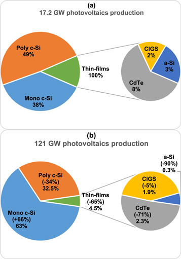
Figure 9. Global PV production of (a) 2010 and (b) 2019.
Download figure:
Standard image High-resolution imageFigure 10 shows the global renewable energy generation capacity in 2019, where the total accounted production was 2,537 GW with an increase of 176 GW (7.4%) than 2018. Corresponding to the statistics by the International Renewable Energy Agency (IRENA), around 583.5 GW (23%) of energy was generated by solar energy sources. The expansion of capacity was led by solar with an additional 98 GW (+20%) comparing the previous term. Moreover, there was 112 MW (among 160 MW increment) off-grid PV energy installation growth based on the preceding period. Regionally, Asia (∼54%) ranked 1st place for overall renewable energy generation, followed by Europe (∼23%) and North America (∼15%) [113].

Figure 10. Global renewable energy generation capacity adapted from [113].
Download figure:
Standard image High-resolution image4. Device property comparison
4.1. Factors of reliability
The reliability to compare the performance of competitive low-cost PV panels is crucial that is determined by factors like Voc, Jsc, and fill-factor (FF). Figure 11 indicates the maximum capacity of solar cells, showing the gradual decrease of output power for c-Si, α-Si, CIGS, and CdTe technologies with increasing temperature from 25°C to 60°C. The relative power loss of c-Si (wafer-based) modules is maximum as the heat escalates, whereas the power reduction of α-Si seems lower than c-Si. On the other hand, CIGS dictates less performance loss than c-Si and α-Si. The CdTe devices depict the capability to hold the best performance as temperature increases [114]. In the case of FF, a downward trend-line is acceptable as the temperature rises for CdTe, CIGS, and c-Si, respectively (from flatter to steeper), however, α-Si provides opposite shifts for single-junction (upward) and multi-junction (downward) [114]. This oddity of α-Si causes for the Staebler-Wronski effect, where a regenerative and beneficial impact happens for the annealing of the cells; prevailing light-induced issues for material degradation [115]. The effect's robustness is connected to the formation of a device because thinner i-layers show lower efficiency loss due to lesser recombination of photo carriers [116]. The temperature coefficient, which exhibits a decreasing trend except for Si-based modules, is important to process PV devices [117]. Furthermore, most thin-films industries cooperate alongside National Renewable Energy Laboratory (NREL) for gathering knowledge on the specifications of market technologies [118].

Figure 11. Maximum capacity of solar cells adapted from [114].
Download figure:
Standard image High-resolution image4.2. Characteristics of devices
Table 7 presents the physical properties of solar cells, summarized as a collective chart. According to the material, structural, and electrical properties; the c-Si, α-Si, CIGS, and CdTe technologies almost gained advantages towards mature fabrication technology. Both CIGS and CdTe modules use some scarce and toxic materials but α-Si and c-Si use earth-abundant and non-toxic substances. However, The CIGS and CdTe cells show a good level of stability regarding temperature but α-Si and c-Si do not hold the balance in due case. With a business value of approximately 132 billion US Dollars ($) [119], the PV industries are growing to concentrate on thin-films by a price range from 0.5 $ to 1 $ per watt [120].
Table 7. Physical properties of solar cells.
| Properties | c-Si | a-Si | CIGS | CdTe |
|---|---|---|---|---|
| Band gap | 1.10 eV [121] | 1.75 eV [122] | 1.48 eV [123] | 1.54 eV [124] |
| Absorption coefficient | >103 cm−1 [125] | >103 cm−1 [125] | >104 cm−1 [126] | >104 cm−1 [126] |
| Temperature coefficient | −0.48%/°C [127] | −0.20%/°C [127] | −0.31%/°C [128] | −0.25%/°C [128] |
| Stability level | less stable | less stable | stable | very stable |
| Toxicity level | non-toxic | non-toxic | less toxic | toxic |
| Material availability | available | available | Ga is available but In is limited | Cd is available but Te is limited |
4.3. Availability of material
The estimated installed capacity growth in 2020 for α-Si is 200 GW/year, CIGS is 70 GW y−1e−1ar−1, and CdTe is 20 GW y−1e−1ar−1 approximately [129]. Figure 12 exhibits the laboratory performance of solar cells, forecasting a trend towards 15%–20% efficient α-Si and 25%–30% of efficiency for both CIGS and CdTe solar cells within the next decade. Due to the dependency on rare-earth, toxic, and less-stable materials, the possibility of large-scale thin-films deployment is limited. However, progress regarding thinner films can eventually lower the necessity of metal by a factor of 10, reducing material requirements [130]. Though there are numerous advantages of CdTe and CIGS over Si-based solar cells, a full dependency on CdTe or CIGS would need more than 75 multiples of rare-element Te or abundant-element Ga production comparing to all PV materials. In regards to CdTe, the yearly generation of toxic-element Cd exceeds the production of Te by a factor of 2 [131]. On the other hand, Ga can eventually be a replacement for rare-element In for producing CIGS [130]. Furthermore, Si is 300,000,000 multiples as available as Te and 20,000 multiples as available as Ga, making it easier to produce Si-based PV panels [131]. On the contrary, effective approaches such as introducing abundant, non-toxic, and more stable materials along with new cell designs to improve performance can guide us towards further technologies on thin films. Additionally, the implementation of PV applications (3% global electricity) impacts climate change in a far more positive way, by saving about 590 million tons of CO2 every year [119].

Figure 12. Laboratory performance of solar cells.
Download figure:
Standard image High-resolution image
According to the overall analogy 6 , it can be inferred that even though thin-films might not be able to substitute commercialized c-Si modules shortly, this technology will have great advantages for most of the Sun-belt nations having high diffused light and humid atmosphere.
5. Next generation technologies
Several new thinner films have surfaced through concentrated research in material science with higher potential, including Dye-sensitized, Perovskite, Organic, Quantum Dot, Plasmonic, Graphene, Sb2Se3-based solar cells.
5.1. Dye-sensitized solar cell
The DSSC belongs to the group of thin-films, functions on a semiconductor generated into an electrolyte and a light-sensitive anode [132, 133]. This material is photoactive that can generate electricity once it is sensitized by light. It traps the photons of incoming sunlight or artificial light and galvanizes electrons by the incident photons' energy. The excited electrons then get into the titanium dioxide (TiO2—a white pigment generally found in white paint) and the injected electron is guided away by nano-crystalline TiO2. To conduct the electrons back into the layer, a chemical electrolyte in the cell closes the circuit and this movement of excited electrons creates energy that can be captured into different types of electrical devices. The primary advantages of DSSC include easier production mostly by the standard roll-printing method using low-cost materials and the almost flexible-transparent device providing different types of applications but unsuitable for glass-based functions. However, practical elimination of several expensive elements has proven to be difficult, notably Pt and ruthenium (Ru), and challenges are being faced to make a device structure suitable for all weather conditions [7]. The energy conversion efficiency of the most recent laboratory-developed module is approximately 12.25% [134]. Though the reported performance is less than the finest thin-film solar cell, theoretically the cost/efficiency ratio of DSSC using dyes should be good enough to challenge fossil fuel power production by acquiring grid equality.
5.2. Perovskite solar cell
The PSC is a perovskite formation-based polycrystalline compound having the formula of ABX3, where A-B indicates the organic-inorganic cation, and X indicates the halide. The most common structure is a compound organic-inorganic lead (Pb) or tin (Sn) halide-based element that works as the photo-collecting functional film. These compound salts create polycrystalline layers consisting of the formulated crystal structure at room temperature through precipitation from different polar solvents. This cell can maintain a bandgap that can be adjusted constantly from pure I to pure Cl, where lower bandgap elements provide greater performance [135]. The elements, like methyl ammonium lead halides (MALHs) as well as all-inorganic cesium lead halide (CsPbH), are simple and inexpensive for production. Other advantages of PSC include low recombination loss [136] and long carrier diffusion lengths [137, 138]. On the other hand, considerably low FF, substantial photocurrent loss, toxic Pb usage, sensitivity to condensation, and instability of these devices are the underlying issues to resolve [139, 140]. The efficiency using the materials reached 28% according to a research-based module, which led it towards the consideration as the fastest-growing solar cell technology to date [141]. Furthermore, large bandgap perovskites functioning as the top layer in the Si-based tandem PSC devices have a higher possibility to enter into the market at lower prices.
5.3. Organic solar cell
The OSC also is known as plastic solar cell generates electricity by organic layer such as poly-acetylene that absorb light and transport charges through the PV effect. The absorption coefficient of light for natural material is excessive, as such, a small number of materials can absorb a large amount of light, with a range of hundreds of nanometers. Due to the potential transparency, the tandem or polymer (typically CN-PPV and MEH-PPV blend) structure of this cell suggests implementations for walls, windows, and malleable devices. The popularity of polymer device research came from the combination of low-price [142] and high-performance [143]. These solar cells are lightweight, disposable, and have less impact on the environment comparing to other technologies. Other advantages of OCS include solution-process-able devices at a high production rate results in low production costs for the fabrication of a large-scale material. The main disadvantages are instability, fragility, and photochemical degradation in comparison with the inorganic Si cells. The best-reported efficiency of this module is 17.35% for the tandem structure [144]. For developing highly efficient and stable OSC, knowledge of charge-separation systems, charge-transport mechanisms, and interfacial consequences of organic materials are required.
5.4. Quantum dot solar cell
The QDSC technology employs solution-processed nanocrystals known as quantum dots for light absorption [145–147]. Generally, the cell functions by a photon of light traveling into the cell and hitting a quantum dot particle resulting in elevation of energy from the electrons. For economical accumulation to near-infrared photons, the size of the quantum dots is needed to be changed, which allows the tuning of colloidal metal chalcogenide nanocrystals bandgap. For processing several portions of the solar spectrum, various types of elements are used to create multi-junction solar cells to improve the efficiency of this technology. Employing lead sulfide (PbS) or lead selenide (PbSe) as the functional layer, the best cell was developed [148]. The advantages of QDSC remain in the air-stable operation and room-temperature fabrication [149] of the quantum dot materials. The maximum efficiency is reported by approximately 16.6% for a lab-scale module [148]. Better knowledge regarding surface chemistry [150–152] and enhancing the middle space phases in the films are required to overcome the current challenges. The mass size of the conventional thin-film materials can be replaced by the quantum dot technology of the QDSC device.
5.5. Additional materials for solar cell
5.5.1. Plasmonic
Plasmonic solar cell converts light into electricity by the usage of plasmon, where the photovoltaic effect can occur either inside the plasmon or another material. Referred to as direct-plasmonic or plasmonic-enhanced solar cells' thickness can vary from 2 μm to 100 nm [153]. The plasmonic-enhanced photovoltaics can be of both perovskite and organic formation to increase its' potentiality. The Design of this cell is primarily 2 types—nano-particle and metal-film, based on the method to trap and scatter light on its surface [154]. With an advantage like having cheaper substrates (glass, plastic, steel) offering improved absorption coefficient and lighter weight, the possibility of its employment is endless, from solar farms to space exploration vehicles. The expected performance of PSC is 40%, where working efficiency as of now is about 10% [155]. Challenges such as destructive interference between the scattered and un-scattered light as well as a scarcity of noble metal nanoparticles are still hampering its progression. By the consideration of commercialization, this technology needs more experimental work to reach its full potential [156].
5.5.2. Graphene
Graphene solar cell consists of an allotrope of carbon having a single layer of atoms arranged in a 2-dimensional (D) honeycomb lattice. Graphene as a nanomaterial is both strong and light that can hold energy better than graphite, due to which it is developed into ARC for photovoltaics. There is a proportional decrease in both optical transparency and sheet resistance with an increasing number of graphene layers. Also, doping of heteroatoms onto a sheet of graphene can significantly alter the chemical, physical, electronic, and photonic properties of the sheet [157]. For excelling in tune-ability and adaptability, it became possible to produce truly flexible, low-cost, and transparent graphene-layered/doped solar cells. Graphene-based organic photovoltaics can offer efficiency as high as 60% theoretically—doubled than any Si-based solar cells. Roadblocks like finding ways of extracting electrical current and enhance absorption of graphene are matters of concern. Although extensive research work to find practical solutions is still underway [158].
5.5.3. Sb2Se3
Sb2Se3 (antimony triselenide)-based solar cell contains a chemical composite with Sb2Se3 formula. The element exists as the sulfosalt mineral antimonselite that crystallizes in an orthorhombic space combination. Its 1D structure with covalently bonded ribbons can be used as an absorber layer with thin-film photovoltaics to enhance performance. However, the current limitation of employment of Sb2Se3 is on single-junction for its greater bandgap. Sb2Se3-based solar cells provide a higher absorption co-efficient and better light management due to their suitable bandgap. Where, photovoltaic conversion efficiency (PCE) of the most recent structure (ZnO:Al/ZnO/CdS/TiO2/Sb2Se3/MoSe2/Mo) is proposed to be 9.2%, composed employing novel compounds. Though carrier management—collection efficiency of photo-generated carriers; requires considerable development. This non-toxic, earth-abundant, and industrially applicable substance gives potential waypoints for making cost-effective and very efficient solar cells [159].
Among the applications of photovoltaic devices, instigation as a power source for automated technologies such as robotics, satellites, and space-crafts are the most promising ones, besides the implementation in grid-connected systems.
6. Conclusion
In this article, 3 major types of thin-film solar cells: α-Si, CIGS, and CdTe were reviewed regarding their sequential developments, structural parameters, and limitations. The best-developed modules along with the global production capacities of these technologies were discussed with analysis. The reliability, properties, and availability of materials for the corresponding technologies were compared. The recorded efficiencies to date for α-Si, CIGS, and CdTe are 14.04%, 23.35%, and 22.1% respectively. In terms of commercialized modules, the performances of α-Si, CIGS, and CdTe are 12.3%, 19.2%, and 19% accordingly. Among these thin films, the CdTe holds the maximum marketplace (2.3%), exceeded by CIGS (1.9%), and α-Si (0.3%) of the whole PV industry. Moreover, the demand for renewable energy regarding solar cells is increasing gradually, which is about 23% as of 2019. On the other hand, CdTe shows the most reliability regarding an elevating temperature. In regards to material properties, availability, and growth; these technologies exhibit some concerns that could be a deciding factor of which technology will apprehend the greater amount of PV requirements in the future.
Solar cell technologies showed the possibility to mitigate future energy demand, but at present, the position of thin films is declining because of the cheap production cost of c-Si devices. Additionally, next-generation technologies such as DSSC, PSC, OSC, and QDSC use abundant elements and simplistic procedures; guiding towards a path for next-level implementations of PV with higher performance. These new technologies are at their R&D phases, so comprehensive progression is required for their commercialization. Among these, the perovskite solar cell looks very promising for developing high-performance (28%) tandem structures with low manufacturing costs. There seems to be a trend that the technologies of the 2nd generation will not only reach the market share of c-Si materials but also get ahead on every aspect, including price and performance. However, due to very little performance and unstable characteristics, large-scale implementations of α-Si devices are not profitable, which is why the business work of this technology is almost obsolete. On the other hand, CIGS technology depicts potential if the limitations regarding material can be resolved along with the reduction in the recombination losses of the device structure. Though correct discarding of Cd is still a problem, CdTe carries on as the main contender of all thin-film technologies. In conclusion, despite the declining marketplace, increasing implementations will empower various technologies of the thin films to flourish soon.
Acknowledgments
The authors gratefully acknowledge the support of the Department of Electrical & Electronic Engineering, Ahsanullah University of Science & Technology, Dhaka, Bangladesh. Additional credits go to Fab Lab Dhaka, Bangladesh for providing the experimental guidance and help.
Declaration of interest
The authors declare that they have no known competing financial interests or personal relationships that could have appeared to influence the work reported in this paper.
Credit author statement
Erteza Tawsif Efaz: Conceptualization, Methodology, Software, Validation, Formal analysis, Investigation, Visualization, Project administration, Writing—Original Draft. Md. Meganur Rhaman: Conceptualization, Validation, Investigation, Supervision, Writing—Review & Editing. Safayat Al Imam: Conceptualization, Validation, Investigation, Supervision, Writing—Review & Editing. Khandaker Lubaba Bashar: Conceptualization, Validation, Investigation, Supervision, Writing—Review & Editing. Fahmid Kabir: Formal analysis, Resources, Data Curation, Writing—Review & Editing. MD. Ehasan Mourtaza: Formal analysis, Resources, Data Curation, Writing—Review & Editing. Syed Nazmus Sakib: Formal analysis, Resources, Data Curation, Writing—Review & Editing. F. A. Mozahid: Software, Visualization, Resources.
Footnotes
- 6
Datasets related to this article can be found at github.com/ErtezaTawsif/Solar, hosted at GitHub.