
Abstract
We present the simulation and experimental demonstration of a coupled-cavity 1D photonic-crystal/photonic-wire (PhC/PhW) structure that produces multiple resonance wavelengths. The combination of several cavities results in the assembly of a spectral response that exhibits multiple resonance wavelengths and potentially leads to the wavelength control required for wavelength division multiplexing (WDM) applications. By using a structure with three distinct in-line cavities, we have obtained three distinct resonance wavelengths—in conformity with the rule that the number of distinct resonance wavelengths is proportional to the number of cavities. The experimental photonic wire waveguide structure had cross-sectional dimensions of 600 nm (width) × 260 nm (height)—with an embedded photonic crystal (PhC) micro-cavity—all based on a silicon-on-insulator (SOI) platform. The embedded PhC structure was tailored to give resonance wavelengths in the C-band and L-band fiber telecommunication range. With the introduction of tapering in the multiple micro-cavity structure, it was possible to obtain three resonance wavelengths that correspond to WDM wavelengths of 1534.87, 1554.63 and 1594.86 nm—whereas, without tapering, the resonance wavelengths were 1645.60, 1670.76 and 1698.68 nm, respectively. We have observed an asymmetric free spectral range (FSR) situation with un-equal resonance wavelength spacing. The taper regions are also responsible for high optical transmission and lower Q-factor values at resonance. Transmission values of 0.17, 0.47 and 0.43 were obtained, together with Q-factor values of 1179.32, 930.05 and 970.35, respectively, without using tapered sections—while transmission values of 0.45, 0.74 and 0.43 were obtained, together with Q-factor values of 1083.24, 850.10 and 885.22, respectively, using tapered sections. (The normalisation values for the experiments were obtained with respect to an unstructured photonic wire). We have demonstrated that the taper structures used must be designed accurately, in order to maximize the transmission values at the desired resonance wavelengths. The demonstration of fabricated device structures that have measured properties that are in close agreement with predictions obtained using finite-difference time-domain (FDTD) computational software is an indication of the precision of the fabrication process. With the introduction of multiple cavities into the structures realised, the number of resonance wavelengths can be tailored for application as WDM components or other wavelength selective filters, such as arrayed-waveguide grating structures (AWGs) and Bragg gratings.
Export citation and abstract BibTeX RIS
1. Introduction
Wavelength division multiplexing (WDM) is currently the predominant technology used for the transport of high bandwidth data [1]. As the demand for large data bandwidth increases, the capital expenditure involved steadily rises. Standard current WDM equipment typically occupies large spatial volumes, due to the bulky nature of components such as filters and multiplexers. As a result, researchers are now investigating smaller footprint devices with higher performance in order to address the large costs involved. Progress in nano-fabrication technology has led to the emergence of high-quality combinations of photonic crystal (PhC) and photonic wire (PhW) structures [2] that are suitable for WDM device miniaturization. The realization of embedded nano-scale holes in silicon photonic wires has brought the accurate manipulation of light to a higher level [3]. Photonic crystals (PhCs) are periodic structures that exhibit photonic band-gaps over defined wavelength ranges and, with the introduction of micro-cavities formed by PhC mirror sections, specific resonance wavelengths can be generated within the band-gap spectral region [4]. Photonic band-gaps are produced by periodic structures with alternating regions that have different (effective) refractive indices interlaced to modify the optical propagation in the medium. Because of the challenges of realizing three-dimensional (3D) photonic crystal (PhC) structures, photonic crystal device research has largely concentrated on 1D and 2D PhC structures. Using 1D PhC concepts, simple and compact structures with strong optical confinement can be fabricated and used as components in the realization of photonic integrated circuits (PICs) [5]. Silicon—a high refractive index (n ∼ 3.46) material that has a clear transparency window at wavelengths from 1200 nm upwards [6]—requires gratings or other structures for exploitation in different applications in the aforementioned wavelength region. Silicon photonic wires have been designed to give strong optical confinement for TE-mode light propagation in structures with an approximately 2:1 width/height ratio [7]—and, with the ready availability of silicon-on-insulator (SOI) technology for integrated photonics applications and SOI wafers with silicon layer thicknesses of 220, 260 and 340 nm, photonic wires with widths of 500 to 700 nm can be fabricated to match the ratio mentioned. The compactness of PhC photonic wires has made this approach a possible solution for the future realization of components for optical interconnects that can replace purely electrical interconnects and thereby potentially overcome limitations associated with Moore's law [8]. Our previous studies on single-cavity photonic crystal structures have shown that the 1D PhC/PhW structures can be designed and fabricated to exhibit quality-factor (Q-factor) values of several hundred thousand [9, 10]. The present study shows that the introduction and control of the taper sections [3, 11] results in a high Q-factor at the designed wavelength, which makes this design potentially suitable for multiple-wavelength device applications. Previous work has shown that having more than a single cavity in a 1D PhC/PhW structure leads to splitting of the resonance wavelengths, in accordance with the number of cavities [12].
2. Device structure
PhC/PhW devices were modelled and fabricated with SOI (top silicon, ∼260 nm, silica, ∼1 μm and silicon substrate, ∼625 μm) in which the refractive index of silicon was assumed to be 3.46, in the wavelength range of interest. The ridge photonic wire structures, with dimensions of 600 nm (width) × 260 nm (height), were supported on a silica buffer layer having an assumed refractive index of 1.45, with air (refractive index 1) surrounding the photonic wire. The selection of wider wire dimensions (600 nm instead of 500 nm [12]) was to have more dialectic material for guiding the light that results in higher optical transmission. The PhC mirror (air holes with 260 nm etching depths) sections had a designed lattice constant of a = 370 nm. The radius of the PhC holes, r , was designed to be 90 nm. The basic structure was repeated as three coupled cavities, each with an inside cavity length of 400 nm cavity, as shown in the simulation schematic of figure 1.
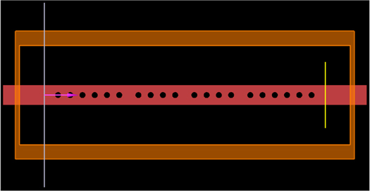
Figure 1. Basic multiple cavity structure with 6-4-4-6 periodic holes divided by cavities.
Download figure:
Standard image High-resolution image3. 3D-FDTD simulation using Lumerical software
Commercial 3D-FDTD software supplied by Lumerical [13] has been used for the device simulation. A compatible layout format is exported for simulation, in order to avoid re-drawing errors. The simulation boundary is specified as a perfectly matched layer (PML). The PML has been chosen so as to absorb all the radiation emitted from the structure, without any reflection back into the simulation area [14]. To perform this simulation, the PML boundaries must be positioned at least half of an operating wavelength away from any part of the structure being modeled—thereby avoiding reflection of the evanescent field from the PML, which would cause a shadowing effect that influences the simulation results. In order to obtain accurate simulation results that closely represent the fabricated device, a 3D version of the FDTD software was selected—and this choice resulted in a significantly time-consuming simulation. But the accuracy obtained is necessary in order to proceed with a proper comparison with experimental results obtained for the fabricated structure. In most simulation packages, the size of the mesh is important for accurate results to be obtained. In the Lumerical software that we have used, a graded mesh approach was used for simulation accuracy purposes as shown in figure 3.
In the simulation, the source used was the 'mode source'—and the mode selected was the TE mode, with a wavelength range from 1200 to 1800 nm. Light was injected at the left side of the device, with propagation in the x-direction. A frequency-domain monitor was used to record the results. In FDTD simulation, a wide range of frequency points is needed to ensure that the whole wavelength response is captured and displayed, but obeying this condition results in a slow simulation process. Figure 4 shows the structure, the PML boundaries—and the positions of both the light source and the monitor represented in the Lumerical FDTD software.
4. Fabrication
The SOI samples were spin-coated with dilute negative hydrogen silsesquioxane (HSQ) resist at 3000 rpm, resulting in a 200 nm thickness coating—and then baked on a hot plate at 90 °C for two minutes, to harden the resist. The sample was then written using an Elionix ELS-F125 electron-beam lithography (EBL) tool with a pattern designed and exported previously from the simulation software. The pattern was written using a 1 nA beam current over a 500 μm2 writing field, with a total of 2 × 10⁵ dots and a beam dose of ∼2500 μC cm−2 that implies a 2.5 nm dot size. The choice of the current used in the EBL process was driven by the requirement for the small dot size involved in writing very precise and small features.
After a sample had been exposed to the scanning electron beam, it was developed using tetra-methyl-ammonium hydroxide (TMAH) at a concentration of 25% in de-ionized (DI) water at 23 °C. The sample was then immersed in the developer for an optimized time of 30 s, aided by mild agitation to reduce the formation of bubbles during the development process. The sample was rinsed in DI water for 60 s to remove the remaining developer—and a double step rinsing stage was required to ensure that any residue (scum) was thoroughly removed.
The developed pattern then underwent reactive ion etching (RIE) to remove the unwanted silicon regions. Inductive coupled plasma (ICP) reactive ion-etching (RIE), using an SF6/C4F8 gas combination, was used to etch out the unwanted silicon, at a flow rate of 30/90 sccm. The chamber pressure used during the etching process plays an important role in giving smooth sidewalls on the fabricated photonic wire structures.
Figure 2(b) shows a top view of the device imaged by using a scanning electron microscope (SEM). As designed with CAD, a GDS file was exported to the EBL tool to be written on the sample prepared. The fabricated embedded PhC structure, in a rectangular cross-section photonic wire with dimensions of 600 nm (width) × 260 nm (height) was then tested and measured optically. The inside cavity length c was, in each case, 400 nm. The first six holes for the first set of PhC mirrors comprised of two identical holes, each with a radius of 90 nm and a lattice constant a of 370 nm, forming one Bragg mirror and another 4 holes that form a taper in the N TI region, with hole radii of 90, 92, 80 and 65 nm, respectively. The distances between these taper holes were 350, 325, 315 and 300 nm respectively. The second set of PhC/PhW mirror structure comprised four holes with radii of 65, 90, 90 and 65 nm, spaced at distances of 310, 370 and 310 nm respectively. In writing a complete device structure, another two sets of PhC mirrors followed periodically as mirror images of the first two.

Figure 2. (a) Schematic structure of the basic photonic crystal wire device fabricated on SOI with silicon wire cross-section dimensions of 260 nm (h) × 600 nm (w). Inset, a top view of multiple-micro-cavity structure with the hole section arrangement to be noted as: front section SF, middle-front section SMF, middle-end section SME and end section SE respectively. (b) SEM image of the fabricated device with lattice constant a = 370 nm; symmetrical cavity, c = 400 nm; mirror radius, r = 90 nm for N number of mirror holes and hole size taper in ( N TI ) for optimization.
Download figure:
Standard image High-resolution image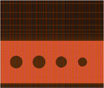
Figure 3. The mesh refinement for accurate simulation that requires high computational power and time in simulation software. In order to have accurate simulation results, the mesh in the circular regions needs to be small by comparison with the smallest feature of the structure and it should increase in size proportionally for bigger simulation regions.
Download figure:
Standard image High-resolution image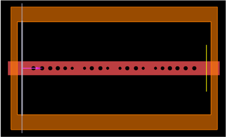
Figure 4. Simulation structure 6-4-4-6 hole-sets separated by 3 micro-cavities with perfectly matched layer as the boundary condition. Tapering is introduced to control properly the transmission level at the resonance wavelengths.
Download figure:
Standard image High-resolution image5. Experimental results and discussion
For an initial design of the device, a basic photonic crystal hole arrangement was designed to have SF-6 holes, SMF-4 holes, SME-4 holes and SE-6 holes—using similar hole radii and separated by equal cavity spacer lengths of 400 nm. Figure 5 shows the simulated response of the basic 6-4-4-6 device structure, with three distinct resonances. Three resonant wavelengths are produced—at 1645.60, 1670.76 and 1698.68 nm respectively, with different resonance peak quality-factor values. Asymmetric FSRs, with values of 25.16 and 27.92 nm respectively, were observed where dispersion quality of the waveguide contributes to the 2.76 nm discrepancies. The splitting of a single cavity resonance wavelength into three distinct resonance wavelengths was due to the number of cavities (three) specified in the structure [15, 16].

Figure 5. Three distinct resonance wavelengths with unequal free spectral range values for 6-4-4-6 holes, respectively (without any hole taper sections), obtained from using the simulation software.
Download figure:
Standard image High-resolution imageThe cavity length in the basic configuration influences the excitation wavelength proportionally; where a shorter cavity length by 50 nm will downshift the wavelength to a shorter wavelength by 50 nm. For example, with 300 nm cavity length, there are 3 resonances in the wavelength range from 1500 to 1610 nm, but with lower transmission values. But whenever mode-matching tapered-hole sections were added, similar downshifted wavelengths were observed—with better transmission performance as compared to reducing the cavity length. Due to the same hole configurations from center of devices, we are expecting equal FSR values but medium imperfection results in different light velocity at different wavelengths (shorter wavelengths travels faster than longer wavelengths). By breaking the symmetrical cavity values, the FSR can be controlled but a complex mathematical algorithm is needed to calculate the parameters that satisfy the maximum device performances.
Figure 6 shows that the quality factor substantially mirrors the transmission values, i.e. the quality factor decreases as the transmission increases—and vice-versa. We obtain transmission values of 0.17, 0.47, and 0.43—together with Q-factor values of 1179.32, 930.05 and 970.35—for resonance wavelengths of 1645.60, 1670.76 and 1698.68 nm, respectively. A higher transmission value typically results in a lower Q-factor value—and vice versa.
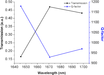
Figure 6. Behavior of the simulated device with respect to the transmission and quality factor (Q-factor), where the values of the two properties are inversely related.
Download figure:
Standard image High-resolution imageAs shown in figure 7, the introduction of taper regions significantly increases the transmission value for most of the resonant wavelengths, due to the light being smoothly guided in the cavity region, with less reflection occurring due to the smoother changes in the effective refractive index and modal distributions between the dielectric (silicon) and hole (air) regions [10]. The whole set of resonant wavelengths has also down-shifted to shorter wavelengths, due to the different group index values obtained after altering the taper mirror radius and lattice constant. With the introduction of tapered hole structures, the Q-factor remains much the same.
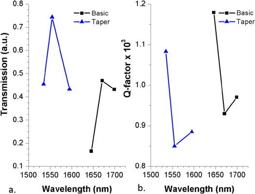
Figure 7. The simulated results as a comparison between a basic hole structure and with hole taper introduced a. the transmission performance that can be seen to have a significant changes due to the introduction of hole taper b. the quality factor (Q-factor) values of the resonance wavelengths.
Download figure:
Standard image High-resolution imageFigure 8 shows the experiment setup where the tunable laser source with a tunable range from 1500 nm to 1630 nm wavelength was connected via a fiber patch-cord to a 'bat-ear' type fiber polarizer—in order to maximize the TE light mode optical power coupled into the device under test (DUT). A lensed fiber was used to guide and focus the light into the cleaved DUT (end-coupled). The output from the device was coupled into a fiber patch-cord via a lensed fiber at the other end of DUT and the output was captured by a fast germanium photodetector monitored via optical spectrum analyzer (OSA).

Figure 8. The experimental setup arrangement with the polarizer placed in between the laser unit and the device under test (DUT), in order to maximize the TE mode linear light transmission.
Download figure:
Standard image High-resolution imageThe PhC/PhW micro-cavity has been designed to produce distinct resonance wavelengths in the C-band and L-band regions, as shown in figure 9. With the structure indicated in figure 4, the simulated resonance wavelengths were at 1534.87, 1554.63 and 1594.86 nm. The Q-factor values obtained for the three wavelengths were 1083.24, 850.10 and 885.22 respectively. The wavelength spacing or free spectral range (FSR) obtained in simulation between the first resonance wavelength and the second resonance wavelength was 19.76 nm while the FSR from the second to the third resonance wavelength was 35.53 nm. The un-equal FSR obtained was due to the resonance wavelengths being governed by the individual cavities in the PhC structure and the summation of the multiple cavity effects in the overall PhC structure. Figure 9 also shows the experimental results with normalized transmission value (i.e. normalized with respect to an unstructured photonic wire). The experimental results agree closely with the simulation, but the intensities differ due to factors that include imperfect device fabrication (reduction of hole size by approximately 10 percent on average from expected initial design) and the surface roughness of the waveguide wall [17, 18]. A fine structure of multiple resonances, with very narrow linewidths was observed in the experimental results. These Fabry–Perot (FP) effects were due to the gap between the lensed fiber used in coupling and the waveguide end [19]—and also due to reflection at cleaved waveguide facets and the mirrors of the PhC cavities [20]. In order to minimize these FP effects, solutions such as using enhanced coupling techniques can be devised. Special optical coatings should be applied on the facets to prevent reflection. Inclined waveguide end facets also reduce such cavity effects [21]. Surface roughness can also reduce FP cavity effects. The number of holes in the PhC mirror sections and hole tapering also impact on cavity effects. Figure 10 shows that the experimental results obtained from the fabricated device are similar to those for the simulation results.
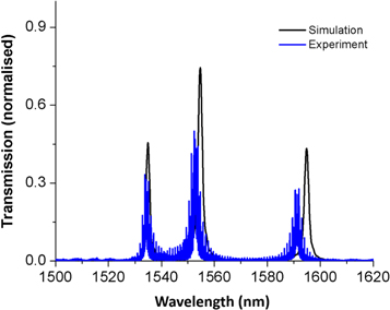
Figure 9. Comparison between simulation and experiment results (where the structure used was the one with taper introduced). The simulated resonance wavelengths were 1534.87, 1554.63 and 1594.86 nm while the experiment resonance wavelengths were 1534.34, 1552.77 and 1591.19 nm respectively.
Download figure:
Standard image High-resolution image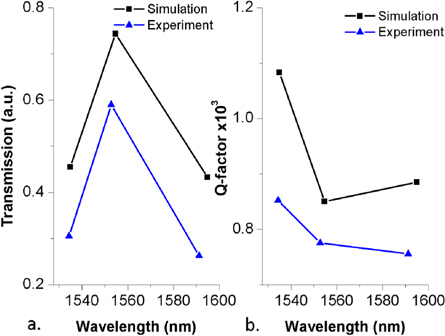
Figure 10. Performance comparison between experiment and simulation. (a) Device transmission at three distinct wavelengths (b) quality factor (Q-factor) versus wavelength.
Download figure:
Standard image High-resolution imageIt is clear that the simulation was accurate enough for the design to be fabricated and that there is substantial agreement between the experimental and simulation results. The performance of the fabricated device deviated from the simulation due to various factors—such as scattering, device imperfections due to fabrication errors—and discrepancies between the single refractive index (RI) value used in the simulation and the RI values at specific wavelengths. To further demonstrate that the design simulated can be used for reliable and accurate fabrication, the same structure, with smaller mirror hole radii of 80 nm (change from 90 nm)—and the same taper structures with variation of the cavity distances—was simulated and fabricated. Figure 11 shows a comparison between the resonance wavelengths of the fabricated device and those resulting from simulation. The experimental results conform closely to the 3D-FDTD simulation results—and the discrepancies are very small, due to the true refractive index value of the material being used for the waveguide and the quality of the device fabricated due to the etching process. The surface roughness of the waveguide wall also plays an important role in modifying the optical confinement. The mesh size will also affect the simulation results. Because of the computer memory limitations involved in simulating the devices, a feasible mesh setting was configured both to provide an adequate simulation and to avoid sacrificing the quality of the results. The transmission values and Q-factors for smaller radii device follows the same trend as the device with 90 nm radii mirror with poorer performances (Q-factor and wavelength separation) due to the weaker mirror configuration.

Figure 11. Comparison between fabricated device results and simulation results, showing that there are only small differences for the excitation wavelengths for both fabricated and simulated devices—and leading to positive expectations for the future exploitation of photonic wire-based optoelectronic devices. Note the use of 'false zeros' for both axes.
Download figure:
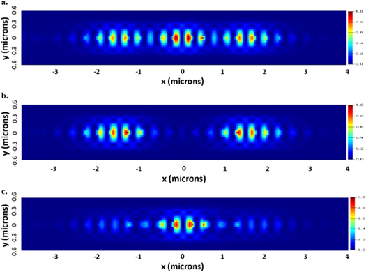
Standard image High-resolution imageThe intensity profiles in figure 12 show how the light is confined in the structure under different resonance conditions and indicates which cavity is primarily responsible for which resonance wavelength. It is obvious in figure 12(a) that all three cavities contribute significantly to the confinement of the 1534.87 nm resonance wavelength. The field profile in figure 12(b) shows that the light confinement for the 1554.63 nm resonance wavelength is primarily in the first and third cavities. For the resonance wavelength at 1594.86 nm, the confinement of the light occurs primarily in the second or middle cavity as shown in figure 12(c). It can be seen from figure 12(a) that the energy for the first resonance wavelength is significantly confined in all three cavities. The intensity distribution at the second resonance wavelength shows that the two cavities on either side of the middle one are responsible for the energy confinement—and, finally, the energy at the third resonance wavelength is confined to the middle cavity.
Figure 12. Intensity profiles of the structure that show the optical confinement in different cavities with respect to the three different resonance wavelengths: (a) the 1534.87 nm resonance wavelength is governed by light being distributed over all three cavities of the structure, (b) the 1554.63 nm resonance wavelength is governed by light distributed over the two outer cavities—and (c) the 1594.86 nm resonance wavelength is governed primarily by light in the center cavity.
Download figure:
Standard image High-resolution image
Jugessur et al [22] have studied the effect of introducing two cavities in a 1D PhC/PhW structure, giving several phase shift regions inside the cavity. The phenomenon of having multiple resonance wavelengths related to the number of cavities has also been observed by Foubert et al [20], with the observed peak splitting being determined by the coupling strength between one single-cavity containing waveguide and another single-cavity containing waveguide that are positioned close together—through controlled variation of the separation distance. This phenomenon can be limited in size due to the number of waveguides needed to produce multiple resonance wavelengths. The similar objective of producing multiple resonance wavelengths that are governed by multiple cavities has been demonstrated by O'Brien et al [23], where—by utilizing ten 2D PhC cavities—ten peaks are predicted in simulation—but there are fewer obvious peaks in an experimental demonstration, due to the limitations of instrumentation capabilities (laser source range)—and, probably, imperfection in the fabricated structure. Another approach to multiple resonance wavelength generation has been reported by Mandal and Erickson [24], where side-coupling with the evanescent light from the main waveguide stripe coupled to the cavity alongside it, embedded in another stripe waveguide. This approach shows more even FSR between resonance wavelengths but results in larger device dimensions by comparison with our approach. These were due to the individual cavity length for different embedded mirror waveguide and the individuals resonant will be side-coupled to the main waveguide. Control of the coupling gap requires to be optimized, in order to minimise the loss and interference by the TM cavity mode. Another side-coupling approach was used by Cluzel et al [25]—with multiple parallel PhC embedded stripe waveguide sections and different cavity lengths for individual waveguide sections being side-coupled to the main bus waveguide at both top (input light) and bottom (output light)—for multiple resonance wavelength generation. The PhC embedded waveguides were designed to have tapered dimension profiles at both ends of waveguides for the light to be maximally guided to the side-coupled waveguide sections with an optimized coupling gap at 100 nm. Again, this approach can be considered to be superior in terms of controlling the FSR of the multiple wavelength resonances generated—with a transmission trade-off to achieve a flatter multiple wavelength response (equal individual transmission amplitude).
6. Conclusions
The results show that, with the advances in nano-fabrication technology now available, accurate fabrication of complex nano-structured devices can readily be obtained. The resonances of micro-cavity structures can be tuned to specific desired wavelengths—whether these are single or multiple wavelength resonances, using the required control of the number, detailed specifications and size of the cavities.
A large resonance Q-factor, together with usefully high transmission values, can be obtained by controlling the dimensions and detailed design of the tapered sections at the edges of the PhC mirror sections—thereby enabling smooth optical propagation through the photonic wire micro-cavity arrangement. The number of holes in each of the cavity-forming mirror sections also impacts substantially on the overall performance of the device. Smaller radius holes will contribute to better overall transmission values and will shorten the forbidden-gap region. It should be noted that the Q-factor is inversely proportional with the transmission value. The suggested smallest hole radius in the experiment was optimized to cater for limitation of etching method in our fabrication technique. We have been able to demonstrate satisfactory agreement between simulation and experimental results. By adding progressively more coupled cavities into PhC embedded photonic wire structures, we have shown that multiple numbers of resonance wavelengths can be introduced that make this very compact photonic device suitable for the next generation of WDM systems and for other applications.
Acknowledgments
The authors would like to thank Ministry of Higher Education Malaysia, The National University of Malaysia and Universiti Putra Malaysia for the facilities and funding given with a grant no LRGS(2015)/NGOD/UM/KPT.