
Abstract
This paper reports a novel shadow mask aligner, which is capable of aligning planar with ∼1 μm alignment error as well as provision to compensate the wedge error by using movements of three precision linear actuators, spotted under optical microscope. The use of three points leveling also overcomes the common error of the upper assembly bending, which could occur with time after its continuous use. The reported wafer/mask holding mechanism is able to accommodate substrates of 3'' to 6'' diameter. The unique magnetic clamping mechanism after alignment has been successfully demonstrated. The fabricated system is useful for alignment of mask and wafer, as well as for other applications like nano-imprint and micro-contact printing lithography. In these cases, moulds/stamp is aligned with the patterned/un-patterned target substrate; to create complex 3D structures micro-assembly of independently fabricated 2D components by proper aligning and clamping.
Export citation and abstract BibTeX RIS
1. Introduction
Shadow masking technique is based on the masking a flux of molecules, ions, atoms or particles to change the substrate surface in particular regions via various techniques namely material deposition, etching or ion implantation [1]. This is a chemical-free patterning method, in which shadow mask are kept between material source and the substrate [2]. While using the shadow masking technology, the crucial part is the accurate alignment of the shadow mask with the patterned wafer/substrate by aligning the features of shadow mask and the target wafer/substrate. Shadow mask alignment system has a number of applications in organic nanoelectronics [3]; in biosensors [4, 5], for integrating the chip over the substrate [6] etc. In another application of laser annealing system, the laser beam is projected through patterned shadow mask over the target substrates [7]. Shadow mask alignment system has also been reported for in situ deposition along with alignment [8]. Normally, shadow mask alignment systems (including commercially available), target substrate/shadow mask are aligned with movements in X, Y, and rotary direction and Z direction is controlled by single micrometer/actuator [9]. A field-by-field alignment technique has been demonstrated for jet and flash imprint lithography [10], this non-widely popular technique is quite suitable for nano-patterning, but not cost effective for micron-dimensional features. In addition, there are few alignment techniques which need more caution/components for alignment e.g. In the reported alignment techniques, before aligning the shadow mask and target substrate, the patterning of self-alignment features over both is essential, basically which needs extra attention to create such alignment features [11–13]. Similarly in another method, shadow mask and substrate are aligned by passing and measuring the light intensity, through grate structures, created in both shadow mask and substrate [14], therefore this technique needs making the grate structures on both substrates as well as light source and detector for measuring transmitted light intensity.
In the available shadow mask aligner system/arrangements, perfect parallelism of shadow masks and target substrate has been assumed [9]. Actually, perfect alignment of the mask with the target wafer/substrate is not likely if the substrate holder or mask holder or both are not parallel i.e. having some tilting error; which is very obvious outcome after their multiple usages. In addition, till now no system is available, which can align wedge shaped substrates (shadow mask/target substrates). In the majority of reported alignment systems, a set of the puck for holding the mask and the substrate is limited to align a fixed and same size (dimension) of the mask and substrate [9]. Even after aligning the mask with the wafer in commercial system, 'nut and bold mechanism' based clamping could break the wafers, which are fragile and having large bow [9].
Here, we report a novel shadow mask aligner, which obviates the drawbacks of the hitherto known methods. The aligner based on independent/combined movements using three precision linear actuators, which are used to make the uniform gap at three locations between shadow mask and planar/wedge substrates, and also to synchronously move the microscope and all the three micro-pushers/actuators. This novel arrangement is capable to carry out multi-level stencil lithography on planar with efficient wedge error compensation mechanism. The specially created grooves in pivots (for three micro-pushers/actuators) restricts the motion of other upper assembly, while movement of single. In addition, the proposed magnetic clamping mechanism provides safety of processed wafers/substrates, results cost saving.
2. A novel shadow mask aligner
The developed shadow mask aligner system is based on novel three points leveling arrangement and is capable of aligning target wafer/substrate accurately with shadow mask for next level of material deposition/etching processes (figure 1). As we started to make the assembly which can be used to align and fix the mask temporary with the wafer, we focused primarily on freedom on tilt, its ability of alignment on multiple levels, its resolution in perfectly aligning the mask, the easiness in handling and also keeping in mind the limitations in dimensions and cost. The complete system includes three precision micro-pushers based movement of upper assembly, which holds the shadow mask. The upper assembly is kept over the pivots of these micro-pushers along with the vacuum holding mechanism for shadow masks. The micro-pushers can be moved up/down independently as well as synchronously with maximum movement of 12 mm with 0.1 μm resolution. Therefore, the shadow mask can be tilted in different directions according to the requirements. The bottom stage consists of manual X, Y stage with 25 mm × 25 mm movements and 2 μm sensitivity, while theta has 360° movements with 0.02° resolution. The target wafer is hold over bottom stage using vacuum.
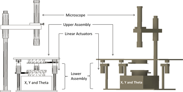
Figure 1. Cross-sectional and isometric view of shadow mask aligner set-up.
Download figure:
Standard image High-resolution imageSingle optical microscope for imaging at three different locations is used to visually inspect and align the dedicated alignment features of shadow mask and target wafer/substrate. In addition, this microscope is also used to estimate the gaps between shadow mask and target wafer/substrate at three locations followed by their alignment. After alignment, both wafer and mask are held together using unique and easy to use magnetic clamping; such clamped sample and mask can be further processed for metallization, etching, lithography, etc.
2.1. Design of upper assembly
Figures 2(a) and (b) depicts complete view of upper assembly, viewed from bottom side and cross-section respectively. Keeping experimental issues in mind and using simple geometrical calculations, the locations of the three pivot holding grooves and vacuum puck are decided in the three points leveling technique.

Figure 2. (a) Back side and (b) cross sectional view of upper assembly of shadow mask aligner set-up. The centre vacuum is used to hold the shadow mask and microscope is used to see through this window using optical microscope. Three specially designed groove structures are made in this upper assembly to hold over three pivots of linear actuators.
Download figure:
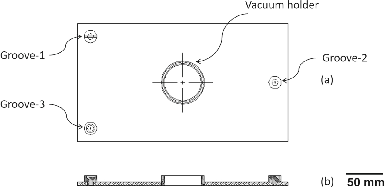
Standard image High-resolution imageThe assembly includes vacuum puck to hold the shadow mask and three specially designed grooved pivot holders groove-1, groove-2, and groove-3 to place the complete upper assembly over three pivots of linear actuators. Figures 3(a)–(c) depicts top and cross-sectional view of the groove-1, 2, and 3 respectively, which is made of stainless steel, machined to make different types of grooves for precise movement control of complete upper assembly using three linear actuators. Groove-1 allows movement of upper assembly in X, and Z direction, groove-2 provides all three degrees of freedom i.e. X, Y and Z, and groove-3 allows assembly movement only in Z direction. These special grooves provide freedom to move all three motors synchronously as well as single linear actuator independently without disturbing others to level the complete upper assembly.
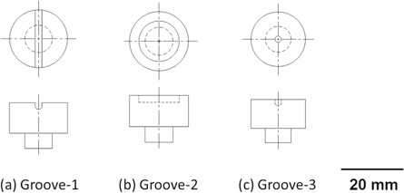
Figure 3. Design (Top and cross-sectional view) of three grooves, made in the upper assembly to be kept over three pivots of linear actuators.
Download figure:
Standard image High-resolution image2.2. Design of bottom assembly
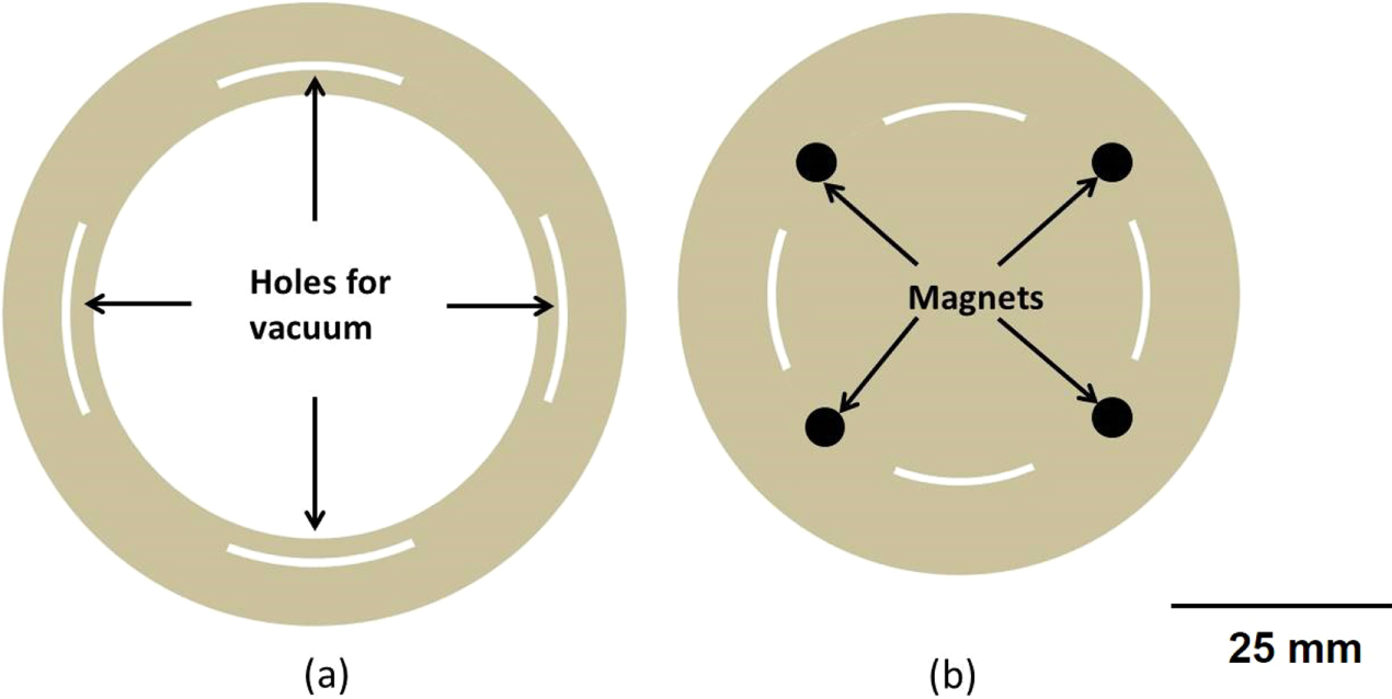
Figure 4 shows designed bottom assembly, having X, Y and theta movement and three linear actuators. This stage is used for movement of the target wafer in XY direction in accordance with the overhead mask wafer. The assembly has vacuum arrangement to hold the target wafer and rare earth magnets fitted in chuck for magnetic clamping. The pivots of three linear actuators are used to hold the complete upper assembly. In the alignment setup the movement of the top assembly based on linear actuators is controlled by using micro-controller for its very fine and smooth movement with resolution of 0.1 μm.
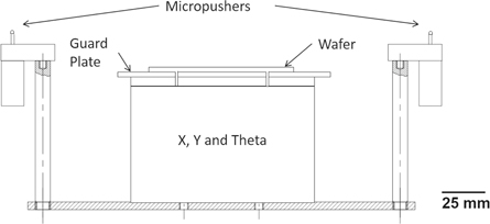
Figure 4. Cross sectional view of bottom assembly of shadow mask aligner set-up. The centre vacuum is used to hold the target wafer through guard plate and three linear actuators are for levelling of shadow mask (in upper assembly) w.r.t. target wafer (in bottom assembly).
Download figure:
Standard image High-resolution image2.3. Wafer holding mechanism, role of guard plates, reliable magnetic clamping, and use of microscope
Figure 5 shows the picture of two plates, which are used as guard plates for shadow mask and target wafer (respectively) as well as for clamping them after alignment. The guard plate is placed under shadow mask, while another is under the target wafer, so that after alignment actually both wafers will be in contact not the guard plates. Shadow mask and target wafers are hold using vacuum via these guard plates. Out of these two plates one is made of ferromagnetic material and another is of magnetic material or consists of permanent magnets/electro magnets, so that after alignment, when both the pucks are brought nearer and vacuum of top shadow mask is released, both plates will get magnetically attached.
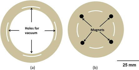
Figure 5. Top view of guard plates, (a) for shadow mask, and (b) for target wafer; used for vacuum holding and magnetic clamping.
Download figure:
Standard image High-resolution imageFigure 6 demonstrates the design of single microscope column assembly, which consists of CCD, lens tube, manual/motorized XYZ movement option, and objective lens. Microscope is not only used for optical inspection during alignment but also to estimate the gap between shadow mask and target wafer at different locations.
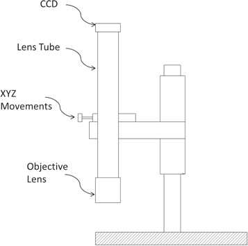
Figure 6. Schematic view of microscope, assembled to align shadow mask and target wafer.
Download figure:
Standard image High-resolution image3. Working of shadow mask aligner
Based on the above design, the system has been realized and the snapshot of fabricated set-up is shown in figure 7(a). First shadow mask is held over upper assembly by vacuum via magnetic plate (figure 7(b)). Then the target wafer/substrate are placed over bottom X, Y theta stage using vacuum via magnetic base (figure 7(c)). The upper assembly is kept over three pivots of linear actuators (figure 7(d)). In this process it has to ensured that there must be sufficient gap between shadow mask and target substrate, before starting the actual alignment process.
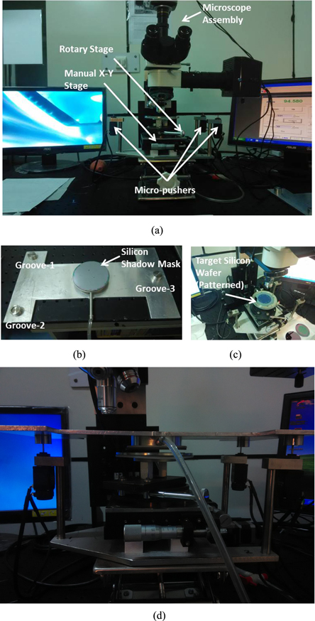
Figure 7. Snapshot of (a) complete fabricated shadow mask aligner set-up, (b) upper assembly holding shadow mask, (c) bottom assembly showing target wafer with vacuum, and (d) after loading upper assembly over three micro-pushers.
Download figure:
Standard image High-resolution imageFirst the gap between shadow mask and target wafer/substrate is estimated using microscope movements. First the three locations on shadow mask near to the pivots are focused and readings of microscope are recorded, say (x1, y1, z1), near to groove-1, (x2, y2, z2), near to groove-2, (x3, y3, z3), near to groove-3. Now after removal of shadow mask at same locations i.e. (x1, y1), (x2, y2), and (x3, y3), now the target wafer is focused and reading of corresponding z is recorded say z1', z2', and z3'. The following calculations are used to estimate the required movement of individual actuator to make them perfectly parallel.
Gap at groov-1, 2 and 3 locations are

Mean of gaps  = (G1 + G2 + G3)/3
Required movement of actuator-1, 2, and 3 is ( -G1), (
 -G2), and (
 -G3). The sign of this value will indicate the movement of upper assembly. Say if we designate positive (negative) for upward, then negative (positive) will indicate downward movement.
According to gap at three locations, the gap is made equal by moving three linear actuators individually/synchronously. Now using microscope and synchronous movement of linear actuators, the upper assembly is moved down, until shadow mask and target wafer/substrate are very near (approximately few tens of microns). After that the features of both are aligned using bottom X, Y and theta movements. Now the upper assembly is moved in fine steps until the gap is very small (of few microns), then the vacuum of shadow mask is released, so the both wafers are clamped smoothly because of magnetic force. Now vacuum of bottom assembly is also released, this clamped assembly is ready for any further process, e.g. deposition, etching, photolithography, etc.
4. Demonstration using silicon shadow mask
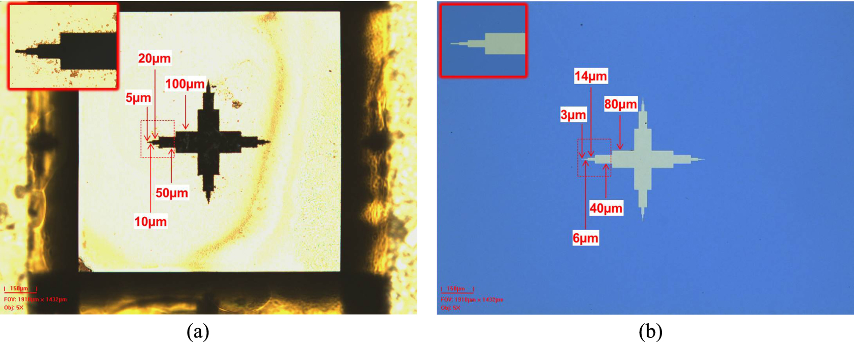
To demonstrate the above mentioned alignment capabilities of designed novel shadow mask aligner set-up, here we used our own fabricated silicon shadow mask (reported separately in [15]) of 3'' diameter with sub-5 μm features and patterned target wafer of 3'' diameter. The first and foremost requirement for alignment is; the shadow mask and target wafer must have alignment marks. As in our case both substrates have cross shaped alignment marks along with fine and coarse features of 5 μm (3 μm) to 100 μm (80 μm) in shadow mask (target wafer). The snapshot of complete alignment marks in fabricated shadow mask and target wafer are shown along with their widths in figures 8(a) and (b) respectively. The zoomed view (marked in dotted red colour box) of the fine features is also shown in inset.

Figure 8. Optical snapshots of cross alignment marks (zoomed box marked in dotted red colour is shown in inset) along with dimensions in (a) shadow mask, and (b) target wafer.
Download figure:
Standard image High-resolution imageThe dimensions of different features of shadow masks are taken purposely larger than that of target wafer to observe easily while alignment under microscope. Using alignment process as described in section III. Figure 9(a) shows the optical image of aligned wafers, while in figure 9(b) the 3D image of depth profile in aligned assembly is taken, in which line profile indicates the depth ∼34.85 μm, measured using Zeta optical profiler. The depth is because of thickness of silicon membrane in shadow mask and bow in both wafers.
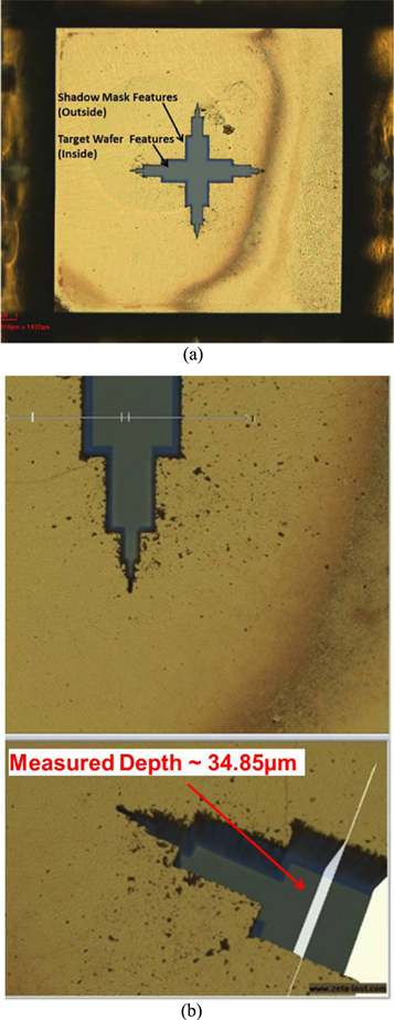
Figure 9. Snapshot (a) of aligned shadow mask and target wafer, and (b) showing 3D picture of aligned part, designating depth ∼34.85 μm which is due to thickness of shadow mask and bow in both wafers.
Download figure:
Standard image High-resolution imageThough under optical microscope (figure 9(a)) it appears that both wafers are perfectly aligned specially misalignment in case of smaller dimensions (≤18 μm (14 μm)) could not be measured.
The alignment error was calculated through measurements of 100 μm (80 μm) features using zeta optical profiler, which is shown in figure 10, it comes ∼1.1 μm in X and 0.3 μm in Y direction. Similarly, it was observed that the 50 μm (40 μm) feature is also almost aligned perfectly in Y direction and with ∼1.2 μm alignment error in X direction.

Figure 10. Measurements of alignment error in aligned assembly of shadow mask and target wafer.
Download figure:
Standard image High-resolution image
5. Conclusion
A novel shadow mask aligner system has been successfully designed and fabricated with alignment error of ∼1 μm. The proposed alignment procedure provides the way to precisely align the shadow mask with the target substrate for multi-level stencil/shadow mask lithography or patterning. The developed system is capable to compensate the wedge error between two wafers; therefore, it can also align the wedge-shaped substrates very easily. In addition, the system can also be used for micro-contact printing and nano-imprint lithography (NIL), where hard contact between mould/mask and target substrate is required and for patterning bio-chemical molecules at specific locations through shadow mask.
Acknowledgments
The authors wish to thank Dr Santanu Chaudhury, Director, CSIR-CEERI, Pilani, India for their keen interest and encouragement. Pankaj B Agarwal is indebted to Prof A Ajayaghosh, Director, CSIR-NIIST, Trivandrum for his valuable guidance. Authors thank Buddh Ram and other members from central workshop for their help and support. Financial support from Council of Scientific and Industrial Research (CSIR), Government of India under CSIR network project is duly acknowledged.