
Abstract
This paper presents a new attenuator bit topology selection algorithm for attenuator design to simultaneously achieve low amplitude and phase error with minimum insertion loss. The significance of this algorithm has been demonstrated by the design and implementation of 8-bit digital attenuator using 65 nm Complementary Metal-Oxide-Semiconductor (CMOS) technology in 2.8 GHz to 4.0 GHz frequency band. To meet the 8-bit attenuation and phase error resolution, new phase compensated Pi-, T- and T-bridge attenuator bit topologies are proposed in place of conventional attenuator bits from 32 dB to 0.25 dB. Performance of this attenuator has been validated with the help of exhaustive post layout parasitic simulation results. The integrated attenuator has demonstrated the highest ever reported attenuation precision at lowest root mean square (RMS) phase error and RMS amplitude error, i.e., 8-bit performance with maximum insertion loss of 5.1 dB, maxmum RMS phase error of 0.78° and maximum RMS amplitude error of 0.1 dB, input referred 1 dB compression point (IP1 dB) > +14.8 dBm, input and output matching <−12 dB, in 2.8 GHz to 4.0 GHz with 1.55 mm × 0.35 mm chip area. This significant improvement in the attenuation precision, RMS amplitude and phase error of the integrated attenuator is the result of, systematic design approach, selection of each attenuator bit architecture using the proposed attenuator bit selection algorithm and incorporation of phase compensation techniques.
Export citation and abstract BibTeX RIS
1. Introduction
Design of the precise amplitude control circuit is very critical in a phased array system. An accurate amplitude control circuit helps in the effective tailoring of beam pattern. Amplitude can be controlled by using a variable gain amplifier (VGA) or a digital attenuator circuit [1, 2]. Digital passive attenuator is always preferred over VGAs in a transmit/receive (T/R) module owing to its bi-directional signal path, simple circuit topologies, ease of implementation, linearity, low power requirement, low phase error and the requirement of simple control circuitry. An active phased array system consists of multiple T/R modules with attenuator. So, it is required that attenuator should have a low RMS amplitude as well as phase error. Accurate amplitude control helps in precise beam steering, scanning and tracking response [3].
Broadly, attenuators are categorized as [3]: distributed, switched path and switched Pi/T attenuators. Distributed attenuators are based on the quarter-wavelength transmission line and varistors [4]. They have very low insertion loss as they do not require any series switch. But distributed attenuator requires highly accurate, area efficient and low phase error quarter-wavelength transmission lines. Switched-path attenuator offers a very low phase error but introduces high insertion-loss since a single-pole double throw switch (SPDT) is used in the signal path [5, 6]. Whereas, switched Pi/T/ T-bridge attenuator circuit [1, 7, 8] topologies offer high linearity [9], are easy to implement and give an option to select among Pi-, T- or T-bridge topologies depending upon the requirement of attenuation. In [9], a T-bridge attenuator has been used for realising a 4-bit attenuator and demostrated high linearity due to use of series-shunt CMOS transistor. In our work, we have chosen to design the attenuator using switched Pi/T attenuator circuit.
Apart from insertion loss and attenuation resolution, phase error is one of the major design challenges in the attenuator realization. It is desired to have low phase-error to achieve better tracking accuracy and minimize the complex phase calibration. Various design techniques have been proposed for compensating the phase error of the attenuator. In [1], a series tail capacitor has been used for compensating phase error introduced by Pi- and T-bridge attenuators, but the T attenuator has not been used with this compensation technique in the design of attenuator. However, this series tail capacitor also affects the attenuation resolution of the attenuator bit, though it can be minimized by using high substrate resistor RS. In [7], additional low-pass or high filter has been used for correcting the phase. However, this additional filter leads to increase in insertion loss and area of the attenuator. In [8], a parallel capacitor has been used with shunt resistor to minimize phase error only in T-topology, while maintaining the insertion-loss. However, there were no reasons for its possible and potential usage for Pi- and T-bridge topologies. In our design, we have proposed new Pi, T-bridge topologies with parallel-capacitor phase-compensation and new T-topology for 0.125 dB attenuator bit with series capacitor for phase compensation, while simultaneously taking care of amplitude error performance.
The main drawbacks of majority of the integrated attenuators [1, 3, 7, 10] proposed in literature are: (i) Non-availability of any reason for selecting circuit topology for a particular attenuator bit by considering the associated realization challenges in CMOS technology and, (ii) insufficient consideration towards technology limitations during the design phase leading to higher insertion loss and RMS phase error. In addition, even after adopting phase compensation, the RMS phase error reported at the integrated level is poorer than expected for N-bit attenuator resolution [3, 7, 10]. For example, in case of N-bit core-chip with N-bit integrated phase-shifter and N-bit attenuator, even though phase shifter RMS phase error is < 1LSB, but if attenuator RMS phase error is > 1LSB, this will degrade the overall core-chip phase response and vice versa. In [11], X-type attenutaor topology has been used for realising 23.1–30 GHz attenuator with LSB of 0.5 dB and used additional compensation circuit to mitigate the process influence. But, in our proposed design, process variation effect has been overcome by use of proposed bit selection algorithm at the design stage without adding any additional circuitry and demostrated the attenuator with LSB accuracy of 0.125 dB.
In this paper, we have addressed the challenges in simultaneously achieving the N-bit amplitude and phase resolution for N > 6 bit attenuator. For achieving the 8-bit amplitude resolution, we have proposed a new bit-selection algorithm and resistor layout matching, and for getting the N-bit phase resolution, we have introduced new Pi-, T-bridge topologies with parallel capacitor for phase compensation and new T-topology with series capacitor for phase compensation. The integrated attenuator is optimized for 8-bit attenuation and phase error accuracy by the use of the proposed phase compensated bit selection algorithm and resistor layout matching technique. The designed attenuator has demonstrated 8-bit attenuation precision with 8-bit phase resolution, i.e., without limiting phase precision of the phased array system severely, with insertion loss < 5.1 dB, RMS phase and amplitude error < 0.78° and < 0.1 dB respectively, in the target frequency-band. The proposed attenuator has the highest ever reported attenuation accuracy at minimum insertion loss, RMS phase and amplitude error. Our work brings out the enhancements in the circuit performance along with the reasoning and justification for selection of a circuit topology for a particular attenuator bit considering process variation and limitation of CMOS technology by means of proposed attenuator bit selection algorithm. This work has, for the first time, introduced the Pi-, T-bridge topologies with parallel-capacitor for phase compensation and new T topology with series capacitor for phase-compensation.
2. MOS switch configuration
In any of the conventional Pi-, T- or T-bridge attenuator topologies as shown in figure 1, CMOS switch comes in the signal path and contribute the most to the insertion loss of the attenuator, which requires to be minimised during the design stage [1].
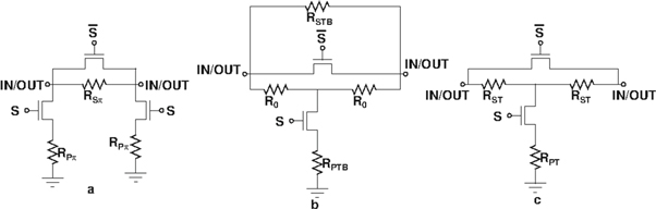
Figure 1. Conventional attenuator (a) Pi- (b) T-bridge (c) T attenuator topologies.
Download figure:
Standard image High-resolution imageInsertion loss of CMOS switch can be decreased by increasing the gate-width of the transistor which decreases on resistance. But this improvement in insertion-loss leads to degradation in isolation, an increase in the device capacitance, an increase in capacitive coupling to the substrate and increase in phase error of the attenuator [12, 13].
Considering the trade-off among insertion loss, frequency of operation and device-width, MOS size was selected by varying the width with frequency. In our design, a high resistance (RG = 20KΩ) has been added in series with gate [13, 14]. This high RG helps in improving the linearity, reducing the variation in MOS on-resistance, improving the isolation between signal and control voltage, reducing the parasitic effect of gate-source capacitance and gate-drain capacitance, and preventing oxide breakdown and signal leakage. And, similarly to minimize the signal loss and capacitive coupling to substrate, a high resistance (RS = 20 KΩ) has been added in the series with substrate [1].
3. Proposed attenuator bit topology selection algorithm
In the attenuator, accuracy of the attenuation level depends upon matching between the resistance used in the reference and attenuation mode. Integrated passive components such as capacitors, resistors etc give 20% or more variation in the actual fabricated chip. Thus, designing the attenuator with high amplitude and phase accuracies is a challenge with components having large process variation and can be overcome by the use of a proper component dimension selection and layout matching techniques. Mathematically, for two matched resistors with width W, resistance R, areal deviation ka and peripheral deviation kp, standard deviation is given by [15].

From the above, it is clear that deviation will be less for the resistor with high value of resistance and/or with large width. Hence, to achieve better matching of simulation and measurement results for the required attenuation level, attenuator bit topology selection is done as per algorithm flow chart in figure 2 and based on the following criteria:
- Absolute value of the series and parallel resistors
- Ratio (R) of the series (RP) and parallel resistors (RS) given by equation (2)
- Possibility of realizing the series and parallel resistors with the same width in a particular bit


Figure 2. Flow chart for attenuator bit topology selection algorithm.
Download figure:
Standard image High-resolution image4. Digital attenuator design
Selection of topology for a particular bit has been made using attenuator bit selection algorithm. For the ideal MOS switch, values of parallel and series resistors used in T, Pi- or T-bridge topologies are given by the equations (3), (4) and (5), respectively [10]


4.1. Design of 16 dB and 8 dB attenuator bit
From equations (3), (4) and (5) we found that, for Pi-attenuator topology in 16 dB and 8 dB attenuator bits, the absolute value of the resistors is the highest, and ratio (R) of parallel and series resistors is minimum. Hence, as per proposed bit selection algorithm, the design of 16 dB and 8 dB attenuator bits were done more accurately using Pi-topology. In order to minimize the mismatch further as per equation (1), both the series and parallel resistors were realized using large width of 10 μm.
To minimize the phase error, a capacitor, in parallel to shunt resistor, has been used in Pi- topology, since it corrects the phase error by introducing phase-lead, without affecting the attenuation state. Figure 3(a) shows the proposed Pi topology used for 16 dB and 8 dB attenuator bits with modified switch configuration and phase compensation capacitor. As a result of these modifications, 16 dB and 8 dB attenuator bits demonstrated 0.15 dB and 0.05 dB attenuation errors, and 0.6° and 0.2° phase errors across the target frequency band, as shown in figure 4. The general terminology for a attenuator bit are, (i) attenuation of a particular bit = Insertion loss of reference state - Insertion loss of attenuating state, (ii) phase error = phase of reference state - phase of attenuating state, and (iii) amplitude error = attenuation of a particular bit - expected ideal attenuation of same bit.
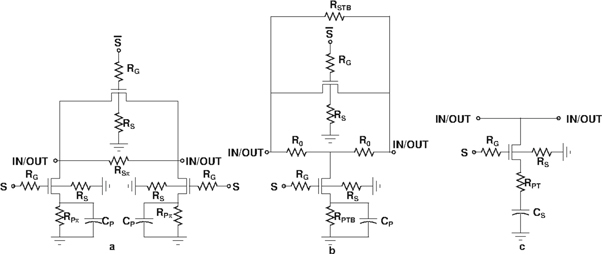
Figure 3. Proposed low phase error (a) Pi (b) T-bridge (c) T attenuator topologies.
Download figure:
Standard image High-resolution image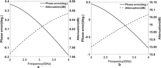
Figure 4. Phase error and attenuation of (a) 8 dB (b) 16 dB attenuator bits.
Download figure:
Standard image High-resolution image4.2. Design of 4 dB, 2 dB, 1 dB, 0.5 dB and 0.25 dB attenuator bits
From the equations (3), (4) and (5) we found that, for T and T-bridge of 4 dB to 0.25 dB attenuator bits, the absolute value of the series resistor is comparatively higher, and the ratio (R) of parallel and series resistors is minimum. As shown in figure 3, in T-bridge topology, only one series resistor is used, but in T topology, two series resistors are used. As per equation (1), for better matching, it has been proposed to use the resistors of same W for all the resistors in a topology. Hence, multiple resistors are used for realizing the small value of resistor in lower attenuation bits. The use of a series resistor in T-bridge topology helps in minimising the layout-area. Hence, for designing lower attenuator bits from 4 dB down to 0.25 dB, T -bridge topology has been used.
Apart from this, T-bridge topology also has better input and output matching due to use of characteristic impedance R0 in the series. Hence, as per proposed selection algorithm, T-bridge topology has been used in designing attenuator bits from 4 dB till 0.25 dB. Similar to Pi-topology, to achieve low insertion-phase, a capacitor parallel to shunt resistor has been used in T-bridge topology. Figure 3(b) shows the proposed T-bridge topology used for 4 dB, 2 dB, 1 dB, 0.5 dB and 0.25 dB attenuator bits with modified switch configuration and the phase compensation capacitor.
As a result of these modifications, these attenuator bits demonstrated less than 0.05 dB attenuation errors, and less than 0.3° phase errors across the target frequency band, as shown in figures 5 and 6(b), (c).

Figure 5. Phase error and attenuation of (a) 1 dB (b) 2 dB (c) 4 dB attenuator bits.
Download figure:
Standard image High-resolution image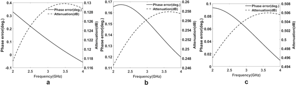
Figure 6. Phase error and attenuation of (a) 0.125 dB (b) 0.25 dB (c) 0.5 dB attenuator bits.
Download figure:
Standard image High-resolution image4.3. Design of 0.125 dB attenuator bit
From equations (3), (4) and (5) we found that the minimum value of resistor required is less than 1 for realizing 0.125 dB attenuator bit using conventional Pi-, T- or T-bridge topologies. To design such a low precision attenuator bit with such a low value of matched-resistor is practically very difficult. So, we have proposed a new T-topology without series resistors. Like conventional Pi-, T- or T-bridge topologies, it is not possible to compensate the phase using a capacitor parallel to shunt resistor since it has phase-lead characteristics. Hence, for reducing the phase error, in this bit, we have introduced phase-lag by using a series capacitor to shunt resistor for compensating the phase-lead. Figure 3(c) shows the design of T topology 0.125 dB attenuator bit. The post-layout simulation result of this proposed 0.125 dB attenuator bit has demonstrated the attenuation and phase error < 0.03 dB and < 0.3° respectively, across the frequency of operation, as shown in figure 6(a).
5. Integrated 8-bit attenuator design
Design of each attenuator bit was started with the initial values of the series and parallel resistors obtained using equations (3), (4) and (5), by taking 50 Ω as characteristic impedance (Z0) of input and output port to minimize the loading effect on integration, and finalized using attenuator bit selection algorithm. To overcome the non-idealities and parasitics effects on integration of attenuator, the values of the series and parallel resistors have been re-adjusted to meet the requirement of absolute attenuation and phase error of less than 1 LSB, i.e., 0.125 dB, and 1.4 degree, respectively, in the frequency band of operation, i.e., 2.8 GHz to 4.0 GHz. All the 8-bits of integrated attenuator have been integrated by keeping S11 and S22 values into consideration in such a way that bits do not get overloaded. In the present design, we have placed the 0.125 dB bit in the centre followed by attenuator bit with the best values of S11 and S22. The bits with the best values of S11 and S22 are kept at the end.
To improve the phase error and input/output matching further, we have used a series inductor between some attenuator bits in the integrated 8-bit attenuator design, as shown in the layout figure [1].
During the integrated post-layout simulation, attenuator bits causing error greater than half LSB, i.e., 0.06 dB were traced and modified. In the post-layout simulation, bond-wire and pad parasitics models were also included to achieve better matching with the fabricated chip. For better RF matching and isolation, all the RF signals were shielded with proper grounding and were routed in top-metal with minimum bends to avoid reflections.
6. Post-layout simulation results and verification
A fully integrated 8-bit passive digital attenuator has been implemented using 65 nm CMOS technology. Exhaustive post-layout simulations were carried out for characterizing the performance of the chip. Figure 7 shows the integrated attenuator chip layout with 1.55 mm × 0.35 mm area.

Figure 7. Full chip layout picture of integrated attenuator with area: 1.55 mm × 0.35 mm.
Download figure:
Standard image High-resolution imageFigure 8 shows the variation of scattering parameters of all the 256 phase states with frequency. In the target frequency band, S11 and S22 are < −12 dB. Figure 8(c) shows the variation of attenuation across the 256 states and the integrated attenuator has insertion loss less than 5.1 dB in the frequency of operation.
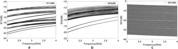
Figure 8. S-parameter of integrated attenuator (a) S11 (b) S22 (c) S21 for all the 256 states.
Download figure:
Standard image High-resolution imageConsidering the process variation and resistor mismatch in any CMOS process, design of 8-bit attenuator with low amplitude and phase error is very challenging. To overcome these problems, detailed analysis was done during the design of each attenuator bit using proposed attenuator bit selection algorithm, and the bit topology selection was done accordingly. To avoid the mismatch, as per equation (1), the high values of resistor and width were used across a particular attenuator bit. By the above steps, resistor mismatch will be same in the reference state as well as in the attenuation state, hence attenuation of the particular bit remains constant. To minimize the effect of process variation in a particular bit, constant width was used for realizing a series as well as parallel resistor.
We could thus overcome the limitation of CMOS process variation and resistor mismatch. We have used shunt or series capacitor in each bit for compensating the lag or lead phase error introduced by the attenuation bit at the frequency of operation.
Figure 9 shows the variation of normalized phase error, RMS phase and amplitude error of the integrated attenuator across the 256 states. In 2.8 GHz to 4.0 GHz, normalized phase error is less than 1.8°, RMS phase and amplitude errors are < 0.78° and < 0.1 dB, respectively. The use of proposed bit selection algorithm and phase compensation techniques have contributed significantly in achieving such a low RMS phase and amplitude errors. Since RMS amplitude error is < 0.1 dB, it can be effectively used as an 8-bit attenuator.
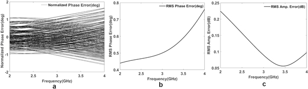
Figure 9. (a) Normalized phase error (b) RMS phase error (c) RMS amplitude error of the integrated attenuator across the 256 states.
Download figure:
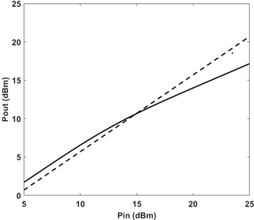
Standard image High-resolution imageIn a typical phased array system [1–3], attenuator is positioned before power amplifier and has power level < 10 dBm. As per analysis across target band of 2.8 GHz to 4.0 GHz and 256 attenuation states, the integrated attenuator has demonstrated minimum IP1 dB of +14.8 dBm at 2.8 GHz and minimum attenuation state, as shown in figure 10, due to inherited linear nature of passive Pi- and T-bridge attenuator topology. However, IP1 dB can be further improved by use of device with higher breakdown voltage or differential circuit as shown in [9].
Figure 10. Input referred 1 dB compression point of the integrated attenuator at 2.8 GHz.
Download figure:
Standard image High-resolution image
Also, the RMS phase error of this attenuator is less than 1.4°, i.e., LSB of 8-bit phase shifter. Hence, this attenuator can be integrated with an 8-bit phase shifter without any degradation of the performance of the later. Table 1 shows a comparison of the designed attenuator performance matrix with other attenuator designs in literature. It can be clearly observed that the designed attenuator has the lowest values of insertion loss, RMS amplitude and phase error with the highest number of precision bits.
Table 1. Performance summary and comparison.
| Reference | [3] | [7] | [8] | [12] | [14] | This work |
|---|---|---|---|---|---|---|
| Technology | 250 nm | 180 nm | 32 nm | 180 nm | 130 nm | 65 nm |
| BiCMOS | CMOS | CMOS | BiCMOS | CMOS | CMOS | |
| Topology | Switched Pi/T With iNMPS | Switched Pi/T | Switched T | Switched Pi/T + distributed | Switched path | Switched Pi/T |
| Frequency (GHz) | 6–12.5 | 8–12 | 10–20 | 10–67 | DC-20 | 2.8–4 |
| Attenuation range (dB) | 16.51 | 31.5 | 16 dB only | 32–43 | 31 | 32.1 |
| No. of bits | 7 | 6 | 1 | 4 | 5 | 8 |
| Max. Insertion loss (dB) | 12.7 | 11.3 | 0.86 | 15.2 | 11 | 5.1 |
| S11/S22 (dB) | >13 | >11 | N/A | >8.7 | >10 | >12 |
| IP1 dB (dBm) | 12.5 | 13 and 15 | N/A | N/A | 10.2 | >14.8 |
| Max. RMS phase error (deg.) | 3.5 | 2.2 | N/A | N/A | 2.5 | 0.78 |
| Max. RMS amp. error (dB) | 2.6 | 0.4 | N/A | N/A | 0.7 | 0.1 |
| Area (mm2) | 0.29 | 0.34 | N/A | 0.77 | 0.5 | 0.54 |
7. Conclusion
This paper presents a design approach for realizing an 8-bit digital CMOS attenuator design with a low amplitude as well as phase error. For better attenuation accuracy, we have used an attenuator bit selection algorithm and selected each attenuator bit topology accordingly. For better phase accuracy, we have, for the first time, introduced Pi- and T-bridge topology with parallel capacitor for phase compensation and a new T topology with series capacitor for phase compensation. Special consideration was given for the device, resistor size selection and layout matching techniques. The proposed attenuator bit selection algorithm provides suitable reasoning and justification for the selection Pi-topology for 16 dB and 8 dB, T-bridge topology for 4 dB till 0.25 dB and T topology for 0.125 dB attenuator bits. The integrated 8-bit attenuator has a chip area of 1.55 mm × 0.35 mm, with the values of input and output matching < −12 dB, IP1 dB of > +14.8 dBm, insertion loss less than 5.1 dB, RMS phase and amplitude error < 0.78° and < 0.1 dB respectively, in the target band of 2.8 GHz to 4.0 GHz.
As per the validated post-layout results, the designed attenuator has the highest attenuation precision bits, the lowest RMS phase and amplitude error in 2.8 GHz to 4.0 GHz. The proposed bit selection algorithm is expected to be very useful for future switched Pi/T attenuator designs.