
Abstract
In this work, a Lookup table based verilog-A model is employed in cadence to evaluate the performance of the chain of inverters and 6-T SRAM cell based on double gate Tunnel-field-effect transistor (DGTFET). In order to drive large capacitance with fixed number of inverters stages with constant width of N type DGTFET (Wn), it is found that the time delay performance of the inverter chain depends on the ratio of width of P type DGTFET of nth stage (Wpn) to width of P type DGTFET of n-1th stage (Wpn−1). Simulation results investigated that the time delay is minimized to 0.265 ns for Wpn/Wpn−1 = 3. The impact of cell ratio (CR) and pull up ratio (PR) on the read stability and write ability of 6-T SRAM cell are investigated by using N curve simulations. It is observed that, increasing CR and PR strengthens the read stability and degrades the write ability of 6-T SRAM cell.
Export citation and abstract BibTeX RIS
1. Introduction
As the technology node is shrinking and number of transistors per unit chip area increasing, hence increasing the standby power consumption [1]. FET devices are operating with steep threshold slope (SS) can be considered as suitable candidate to overcome the power dissipation across the integrated circuit modules. The excellent switching characteristics and steeper sub-threshold slope makes double gate field effect transistor (DGTFET) a promising candidate for the replacement of bulk MOSFETs [2]. Tunnel FET can be considered as a reliable low power device which possesses the property of lower SS < 60 mV/decade due to the band to band tunneling transport process [3, 4]. The reported low values of IOFF ∼1 × 10⁻¹⁴ A −1 μm−1 makes the DGTFET suitable transistor in order to reduce standby power consumption in integrated circuits. In section 2, a double gate TFET of 30 nm gate length with HfO2 as gate dielectric is simulated by considering non local band to band tunneling model in order to obtain I-V and C-V characteristics and later used to develop the look up table based Verilog A model [5–9]. All the device level simulations are done in Sentaurus 2D [10].
Apart from the device behavior of DGTFET, it is important to analyze the performance of DGTFET based integrated circuits. It is difficult to obtain compact analytical model for emerging FET devices to carry out the circuit simulations and DGTFET is one of them. However, the suitable way to carry out the circuit simulation is by using look up table based verilog A model which is capable to capture and analyze dc and transient behavior of the emerging FET devices [11]. The Verilog-A model is coded in the Cadence and then used for DGTFETs based circuit design and simulations. The model is composed of 2D table: the transfer characteristics Ids (Vgs, Vds), the gate-source capacitance Cgs (Vgs, Vds) and the gate-drain capacitance Cgd (Vgs, Vds). Once the symbol for the DGTFET generated, NAND and NOR gates are simulated to validate the model from the characteristics mentioned in section 2. This paper is focused on analyzing the reliability and validity of verilog-A model by evaluating the performance of DGTFET based circuits.
Semiconductor chips built of various circuit modules that are placed distant apart on the chip area. All modules are connected to each other by interconnects. The interconnect length between the modules contributes the parasitic capacitances and behaves as a transmission line which enhance the signal propagation time from one node to another node results in propagation delay across interconnects. Literature shows that the propagation delay between the electrical nodes can be minimized by using repeating network of inverters called as chain of inverters [12, 13]. The performance of the chain of inverters is significantly affected by the number of the inverter stages and the sizing of the inverters. Therefore for the fixed number of inverter stages across two nodes, the signal propagation delay can be minimized by choosing optimum value of inverter stage size ratio (b) i.e. sizing of each nth stage inverter is 'b' times the sizing of n-1th stage inverter such that (Wp/Wn)n = b(Wp/Wn)n−1 , where 'b' is inverter stage size ratio and Wp and Wn are termed as width of P type DGTFET and N type DGTFET. The performance analysis of the Double gate Tunnel FET based chain of inverters for various stage size ratios is discussed in the section 3.
Memories are one of the most important chip areas to store the binary data. To retain the stored data indefinitely, it is necessary for memory circuit to be static. The data storage cell, i.e. the one-bit memory cell in the static RAM arrays, consists of a simple latch circuit with two stable operating points [14]. Depending on the preserved state of the two inverter latch circuit, the data being held in the memory cell will be interpreted either as logic 0 or as logic 1[15]. The data storage capability, read stability and writes ability of the 6-T SRAM depends on the size of access transistors, therefore N-Curve simulation method is used for the performance analysis of the 6-T SRAM cell for various cell ratios and pull up ratios and same is discussed in sections 4 and 5.
2. TCAD simulation and Look-up table based Verilog-A model of DGTFET
An proposed double gate TFET (DGTFET) device structure is shown in figure 1 employed for TCAD 2D simulations. Metal gate work function near about 4.2 eV yields higher amount of on current ION [16]. Application of high-k gate dielectric material improves the gate control and internal electric field in the device, resulting in lower tunneling width with high ION current and low IOFF current [17, 18]. Fermi statistics, non-local band to band tunneling model and Shockley-Read-Hall (SRH) recombination model with Poisson and carrier continuity equations are coded in TCAD (Technology Computer Aided Design) script to achieve device simulation. Post simulation results shows current-voltage (I-V) characteristics of the DGTFET as mentioned in figure 2(a) which reports the SS ∼ 15 mV dec−1. The TFETs possess SS < 60 mV dec−1 and has potential to reduce the power consumption [19].
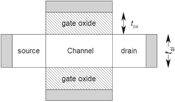
Figure 1. Device structure of DGTFET.
Download figure:
Standard image High-resolution image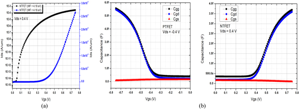
Figure 2. (a) I-V characteristics of NDGTFET. (b) C-V characteristics of N type DGTFET and P type DGTFET.
Download figure:
Standard image High-resolution imageIn this paper, a hetrojunction TFET and plasma based doping less TFET (CP-DLTFET) [20] are compared with the propped DGTFET. The performance parameters of various TFETs are listed in the table 1. A slightly asymmetrical hetero junction TFET device structure with an abrupt doping profile between the source and the drain resulting device gate length of 30 nm is reported in reference. The AlGaSb material is used for the source, and the channel and drain were made of InGaAs. The proportions of the materials in the bandgap were tuned to have roughly aligned valence bands. The doping concentrations were as suggested in the reference design, with 2 × 10¹⁹ atoms/cm3 boron doping in the source, 5 × 10¹⁹ atoms/cm3 arsenic doping in the drain, and 5 × 10¹⁵ atoms/cm3 arsenic doping in the channel.
Table 1. Performance parameters of the different type of TFET structures.
| S. No. | TFET devices | ION (A) at Vgs = 0.75 V | IOFF (A) | SS (mV dec−1) | ION/IOFF |
|---|---|---|---|---|---|
| 1 | Hetrojunction TFET [20] Gate length = 30 nm | 3 × 10⁻⁸ | 2 × 10⁻¹² | 71 | 1.5 × 10⁴ |
| 2 | SGOI (Lg = 30 nm) [21] | 1 × 10⁻⁶ | 1 × 10⁻¹⁴ | 37 | 1 × 10⁹ |
| 3 | TFET (CP-DLTFET [22] Channel Length = 30 nm | ∼4 × 10⁻⁶ | 1 × 10⁻¹⁷ | 15.4 | 4 × 10¹¹ |
| 4 | Si Double gate TFET (Lg = 30 nm for this paper) | 4 × 10⁻⁴ | 1 × 10⁻¹⁴ | 15 | 4 × 10¹⁰ |
Another TFET structure in which germanium is used as a source because of low band gap material and silicon germanium on Insulator (SGOI) is reported in reference [21]. TCAD Simulation predicted the high ION/IOFF ratio and steep sub-threshold swing which are reported in above table. The reported structure is capable of increasing the speed of the transistors by straining the crystal lattice, resulting in improved electron mobility and optimal drive currents.
From the above discussion and the performance parameters listed in above table, it can be easily predicted that the proposed Si TFET structure has better ION/IOFF ∼ 4 × 10¹⁰ and steeper SS ∼ 15 mV dec−1. Proposed structure can be realize as promising candidate to carry out the low power circuit applications.
The parameters considered to carry out the 2D TCAD simulation are listed in table 2. The small signal AC analysis at 5 MHz has been performed in TCAD to carry out the capacitance-voltage (C-V) characteristics of the DGTFET as shown in figure 2(b). Gate to grain capacitance (Cgd) closely following the gate capacitance (Cgg) all over the gate voltages due to charge coupling between source and drain caused by band to band tunneling mechanism in DGTFET [23].
Table 2. Physical Parameters of Double gate tunnel FET.
| DGTFET parameters | NDGTFET (Si) | PDGTFET (Si) |
|---|---|---|
| Channel Length (Lg) | 30 nm | 30 nm |
| Channel Width | 1 μm | 2 μm |
| Doping :Source Region | 1 × 1020 cm−3 (B) | 1 × 1020 cm−3 (P) |
| Doping: Channel Region | 1 × 1016 cm−3 (B) | 1 × 1016 cm−3 (B) |
| Doping :Drain Region | 1 × 1020 cm−3 (P) | 1 × 1020 cm−3 (B) |
| Oxide Thickness (tox) | 1 nm | 1 nm |
| Body thickness (tsi) | 7 nm | 7 nm |
Body dielectric 
|
11.8
|
11.8
|
Oxide dielectric
|
21  (HfO2) (HfO2) |
21  (HfO2) (HfO2) |
DGTFET is an emerging device and therefore, very few analytical models are available. Therefore, look up table based Verilog-A model is used for the integrated /mixed circuit simulation. Due to the ongoing efforts of P type DGTFET development, almost identical drive-currents, Ids (Vgs, Vds) same as N type DGTFET is considered for P type DGTFET for simulation purposes [24]. The Verilog-A module is then used as instances for circuit simulation in cadence spectre. To validate the Verilog- A model of DGTFET, the universal logic gates (NAND and NOR) are constructed and verified by the results as shown in figure 3 and it is validated that now the look up table based Verilog-A is ready for circuit simulations. The voltages overshoots are noticed during the logic response of the gates are due to dominant effect of miller capacitance at the drain node of DGTFET [25].
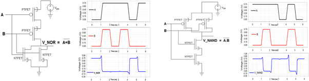
Figure 3. NAND and NOR gates outputs to validate the verilog A based look up table model.
Download figure:
Standard image High-resolution image3. DGTFET based inverter chain simulation and its performance evaluation
This section includes the circuit simulation of chain of inverters consisting of three stage inverters driving the fourth stage inverter which is acting as a load. Let us consider that the chain of 4 DGTFET inverters as shown in figure 4(a), where 4th inverter acting as a load whose large gate capacitance (Cg4 = CL) needs to be driven by the previous three stages of inverters. It is shown that sizing of each nth stage is 'b' times the sizing of n-1th stage such that (Wp/Wn)n = b(Wp/Wn)n-1 , where 'b' is inverter stage size ratio, Wp and Wn are termed as width of P type DGTFET and width of N type DGTFET. It is assumed that the fan out f = Cgn/Cgn−1 for each stage and, where Cg is the gate capacitance of the inverter and f of each stage is given by fN = F, where F is over all effective fan out and given by CL/Cg1 which is same as Cg4/Cg1 (4th stage act as a load) and N (3) is number of stages driving the load (4th stage). It is known that the gate capacitance is directly proportional to the width of the P type DGTFET and N type DGTFET so fanout can be also given by f = (Wp/Wn)n/(Wp/Wn)n−1. The whole idea here to optimize the inverter stage size ratio (b) for a given number of inverter stages to achieve minimum delay across the nodes, Vin and VOUT. It is found that f = b from the above discussions. For the inverter chain simulation, it is considered that the width, Wn =1 μm of the N type DGTFETs and remains fixed in every stage, on other hand the width of the P type DGTFETs is only varied in each stage to investigate the impact of inverter stage ratio (b) i.e. b = f = becomes (Wp)n/(Wp)n−1.

Figure 4. (a) Chain of 4 DGTFET inverters along with 4th inverter acting as a load. (b) Total Delay versus Inverter stage size ratio (b) characteristics.
Download figure:
Standard image High-resolution imageFigure 4(a) shows chain of inverters, where Cg4 of 4th stage acting as a load capacitance (CL) and first three stages are driving the CL. The width (Wp = 54.36 μm, Wn = 1 μm) of 4th stage inverter remains fixed to maintain the Cg4 constant throughout the simulations to investigate the impact on propagation delay between Vin and VOUT for various inverter stage size ratio (b). From the figure 4(b), it can be seen that there is a drastic decrement in propagation delay (3.04 ns → 0.35 ns) is noticed for stage ratios b = 1 → 2. Afterwards, the delay is minimized at 0.265 ns for b = 3. Table shows listed values of Wp for all the P type DGTFETs for different stage size ratios and their I-V sand C-V sets of simulated data were used for look up table and coded in verilog-A to carry out the inverter chain simulations.
The above results and analysis can be explained by the equation (1)–(4). Minimum path delay /propagation delay (tp) between Vin and VOUT is given by equation (1) where N is the number of stages driving the CL (4th stage as a capacitive load), F is the effective fanout (CL/Cg1 ∼ Wp4/Wp1), tpo is propagation delay across each stage without any external load and γ is the processing parameter [26].

For a given load, CL and fixed number of driving stages, N; the computed optimal sizing fopt, at which delay is minimum is mentioned below [22].


From the results shown in figure 4(b), the obtained value of fopt is 3 and the calculated value of processing parameter (γ) is 0.295 which is lies between 0 and 1 (γ = 0 for no self loading and γ = 1 for self loading conditions) The 0.295 value of processing parameter shows that there may be the partial self loading for the inverter due to miller effect of Cgd at the drain node of each DGTFETs Therefore it can predicted as the band to band tunneling couples the gate charge to the drain side which tends Cgd to follow Cgg (shown in figure 2(b)), hence increases miller capacitance at the drain node which results in partial self loading for the DGTFET inverter and results the processing parameter, γ = 0.295.
4. DGTFET based 6-T SRAM cell simulation and its performance evaluation
To retain the stored data indefinitely, it is necessary for memory circuit to be static. The data storage cell, i.e., the one-bit memory cell in the static RAM arrays, consists of a simple latch circuit with two stable operating points. Depending on the preserved state of the two inverter latch circuit, the data being held in the memory cell will be interpreted either as logic 0 or as logic 1 [27, 28]. This section discusses about read and writes process in the cell and its experimental setup. The read and write performance of the 6-T SRAM is basically affected by the sizing of the transistors (Cell Ratio, Pull up Ratio). In order to analyze the read stability and write ability of 6-T SRAM cell, N-curve simulation method is used [29]. N-curve is capable to describe the complete functional analysis of the SRAM cell terms of performance affecting parameters given by static current noise margin SINM, static voltage noise margin SVNM, write trip voltage WTV and write trip current WTI. Prior to N curve simulations it is important to carry out read and write simulation based study of 6-T SRAM cell in order to validate the verilog A model and same is mentioned in sections 4.1 and 4.2.
4.1. Read operation of 6-T SRAM cell
To achieve high memory density, it is necessary to keep size of SRAM small as possible. Optimized sizing of the latch structure is one of the critical parameter for reliable operation of the cell. Figure 5(a) shows schematic of a 6T DGTFET SRAM and figure 5(b) shows equivalent circuit during the read operation. To access the data in the memory cell at node Q or Qbar, the select line is enabled and it controls the two access transistors M5 and M6 shared between read and write operation. Q and or Qbar are complemented nodes to each other. Lets the initial state of the cell is Q = 1 and Qbar = 0 logic. Prior to the read cycle begins, the BL and BLB bit lines are pre-charged to logic 1 by considering the initial charge on capacitance, Cbit (0.1 pF) = 0.75 V. To proceed the ready cycle, the select line is enabled with logic 1 to turn on the access transistors, M5 and M6 (N type DGTFETs) which results in discharging of BLB and at the same time node Qbar starts charging [27, 30]. The rising voltage at Qbar must be lower than the threshold voltage of M3 to avoid accidentally writing logic 1 into the cell. In order to avoid the data flipping in the cell, the resistance of M5 must be larger than resistance of M1 and this can be done by proper sizing of M5 and M1. Read operation of 6-T SRAM cell is analyzed by the circuit simulation by initially setting the node Qbar = 50 mV for logic 0 and Q = 0.75 V for logic 1 for the cell ratio, CR = (W1/L1)/( W5/L5) = 1.5 and results are shown in figure 5(c).

Figure 5. (a) Schematic of DGTFET 6T SRAM cell. (b) Read equivalent of DGTFET 6T SRAM cell. (c) Read operation of DGTFET 6T SRAM cell.
Download figure:
Standard image High-resolution imageFigure 5(c) shows that initially up to 0.2 ns, the select lines are not activated which pushes the access transistors M5 and M6 in off state so that Qbar initially tries to discharge upto a 25 mV through M1. Between 0.2 and 0.4 ns, the select line changes the state from 0 to 0.75V (enable state) which turns on access transistors and forces the node Qbar (V_Qbar) to charge up to 225 mV. At this state, Qbar is below the threshold voltage of M3. On other hand, BLB starts charging and bit line voltage (V_BLB) discharges by 135 mV. After 0.4 ns, the select lines are in disable state and node Qbar starts discharging through M1 and the voltage across BLB is maintained at 615 mV. The final voltage across bit line BLB is sensed by the sensor amplifier of TFET technology as mentioned in reference [31] to complete the reading process of the cell. The read delay for the 6T SRAM cell is calculated to 0.1 ns according to [32].
4.2. Write operation of 6-T SRAM cell
During the write operation it is assumed that the initial state of Q = 1 and Qbar = 0. A logic 0 is to be written in the cell b setting BLB = 1 and BL = 0 logic as shown in figure 6(a). This causes the flip-flop to change state if the devices are sized properly. Note that Qbar node of the cell cannot be pulled high enough to ensure the writing of 1. Therefore the new value in the cell has to be written through transistor M6. To understand the write operation, the nodes Q and Qbar are initially set at 0.75 V and 0 V which is similar to logic 1 and logic 0 at these nodes. In order to write logic 0 in this cell, the select line are activated to turn on the access transistors. Node Q starts to discharge through M6. A reliable writing of the cell is ensured when the node Q pulled down low enough, i.e., below the threshold voltage of the transistor M1 so that M1 gets turned off and stop discharging node Q . Therefore, the voltage of node Qbar rises through M5 and this rise in voltage will flip the content stored in the cell. The new states of node Qbar and Q are logic 1 and 0 [26–30].
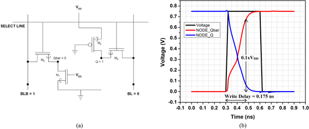
Figure 6. (a) Write equivalent circuit of DGTFET 6T SRAM. (b) Write operation of DGTFET 6T SRAM.
Download figure:
Standard image High-resolution imageFigure 6(b) shows the simulated results for write operation in SRAM cell for pull up ratio (PR = 1.5, defined by (W4/L4)/(W6/L6)). During the off state of voltage cycle, initially from 0 ns to 0.2 ns; the access transistors M5 and M6 are in off state and do not conduct current and unable to charge the node Qbar from 0 V to higher voltages so that Qbar remains at state of 0 V. Between 0.2 and 0.4 ns the access transistors are in on state and force the node Q to discharge through M6 and transistor M1 gets turned off so that node Qbar voltage start rising which flips the content in the cell. After 0.4 ns the new content in the cell is written as, node Q = logic 0 and Qbar = logic 1. The write delay for the 6T SRAM cell is calculated to 0.175 ns according to reference [32].
5. Read stability and Write ability analysis of 6-T SRAM Cell
A voltage sweep, Vin (from 0 − 0.75 V) is applied at Qbar (logic 0 storing node) and the source current (Iin) is measured for analysis of the cell performance is shown in figure 7(a). For the circuit simulation of SRAM cell, the operating voltage range is considered from 0—0.75 V. TFETs are unidirectional devices; however its unidirectional property does not place restrictions on reading ability of SRAM cell. In this paper, the access transistor is chosen in inward direction as a result, a write operation performed by the single access transistor (M5) may degrades the write ability of the cell but improves the read stability of the cell. The simulation results also show consistency with this statement.

Figure 7. (a) Set up for N curve analysis. (b) N curve of SRAM for stability analysis.
Download figure:
Standard image High-resolution imageTo understand the behavior of simulated N-curve shown in figure 7(b), let's consider the Kirchhoff's law at node Qbar of the SRAM cell (Iin = IM1-IM5), where IM1 and IM5 are the drain currents in the transistors M1 and M5. Sweeping Vin continuously changing the operating regions of the SRAM cell, resulting in N-curve. At Vin = 0 V, the transistor M5 is in saturation region and transistor M1 is linear region which results in IM5 > IM1, therefore that current (Iin) is negative at this point. At point 'A', current IM1 = IM5 which results in Iin = 0 A. After the point 'A' with increase Vin, the IM1 slightly becomes greater than IM5, sign of Iin changes from negative to positive and further increment in Vin from point A to B, Iin reaches to the maximum value, the maximum Iin known as static current noise margin (SINM). SINM is defined as the maximum value of DC current that can be injected in the SRAM cell before its content flips [33, 34]. The voltage difference between point A and B indicates the maximum tolerable DC noise voltage at the node Qbar before its content flips. This is due to the fact that after point B the sign of the current changes. The voltage difference between the points A and B is termed as static voltage noise margin (SVNM) [35, 36].
Further increasing voltage beyond the point B, Iin changes sign from positive to negative and achieve the negative peak value between pint B and C, known as write-trip current (WTI). WTI is the amount of current needed to write into the cell when both bit-lines (BL and BLB) are kept at VDD. On the other hand, the lower the absolute WTI, the higher is the write-trip point of the cell. Similarly, the voltage difference between point C and B or the write-trip voltage (WTV) is the voltage require before the changing of the content of the internal node (Q = 1) of the cell [37, 38].
It can be understood as, SVNM and SINM gives the read stability of 6-T SRAM cell simultaneously WTV and WTI provides the information for write ability of SARAM. Higher the static noise power margin (SPNM = SINM*SVNM), higher is the read stability and lower the write trip power (WTP = WTI*WTV), higher is the write ability of the cell [35]. 6 T SRAM cell is simulated to obtain N curves for various cell ratio (CR = 0.5 → 2) and pull up ratio (PR = 0.5 → 2) in order to analyze the read stability and write ability.
From the figures 8 and 9, it can be seen that the read and write operations of a 6T SRAM cell are affected by the cell ratio and pull-up ratio respectively [36]. SINM and SVNM increases with cell ratio (CR), the SRAM shows better read stability at higher values of CR. Apart from this, the computed values of SNPM (μW) = 0.242, 1.51, 7.76, 14.5 and shows improvement in the cell read stability with CR. It is desired to have higher values of SVNM and SINM to achieve better read stability, hence CR = 2 is a preferable sizing where SNPM (14.5 μW) is maximum. Increment in WTP (μW) = 0.36, 1.34, 4.76, 5.94 for CR = 0.5, 1, 1.5, 2 respectively are noticed. For the write-ability of the cell it is preferable to have a small WTV and a small absolute WTI and in order to achieve it, CR = 0.5 shows good agreement with WTV and WTI, hence preferable value of WTP is 0.36 μW at CR = 0.5. Increasing CR increases the WTP which degrades the write ability of the cell [35, 36]. From figure 6(a) it can be seen that access transistor M5 cannot pull down the node Qbar since it conducts only in inward direction. Therefore, access transistor M6 must pull up the node Q without any assistance from the access transistor, M5, to well above the trip-point voltage of the inverter (formed by M2 and M1). As a result, a write operation performed by the single access transistor may substantially worsen the write ability or, in other words, significantly reduce the Write ability of the cell. Figure 9 and table 3 show the cell performance parameters affected by pull up ratio (PR) and values of SNPM (μW) = 1.58, 5.96, 11.5, 17 and WTP (μW) = 0.938, 1.84, 3.59, 5.31 for PR = 0.5, 1, 1.5, 2 respectively are computed to analyses the read stability and write ability. The highest SNPM (17 μW) is noticed at PR = 2 and lowest WTP (0.938 μW) is noticed at PR = 0.5. So from the simulations, it is observed that the highest value of PR = 2 is preferable for the read stability and for the write ability, the preferable value of PR = 0.5 where WTP is minimum (0.938 μW). On the basis of above calculations it can be seen that there is a trade off relationship SNPM and WTP [37–39]; the read stability shows good agreement with CR and PR but on other hand the SRAM is losing the write ability with CR and PR.
Table 3. Fanout (F) for various inverter stage size ratios (b) for different width of P DGTFET and propagation delay variations with 'b'.
| Showing P type DGTFET width sizes for various inverter stage size ratio (b) | Showing total delay estimation across Vin and VOUT | |||||||
|---|---|---|---|---|---|---|---|---|
| DGTFET Inverter stage Ratio | Effective fanout, F | 1st stage Wp1 | 2nd stage Wp2 | 3rd stage Wp3 | 4th stage Wp4 | THL | TLH | Total Delay (THL + TLH)/2 |
| b = f = 1 | 1 | 54.36 μm | 54.36 μm | 54.36 μm | 54.36 μm | 3.08 ns | 3 ns | 3.04 ns |
| b = f = 1.5 | 3.375 | 16.10 μm | 24.16 μm | 36.24 μm | 54.36 μm | 1.06 ns | 1.04 ns | 1.05 ns |
| b = f = 2 | 8 | 6.79 μm | 13.59 μm | 27.18 μm | 54.36 μm | 0.36 ns | 0.34 ns | 0.35 ns |
| b = f = 2.718 | 20 | 2.718 μm | 7.385 μm | 20 μm | 54.36 μm | 0.36 ns | 0.22 ns | 0.28 ns |
| b = fopt = 3 | 27.18 | 2 μm | 6.02 μm | 18.12 μm | 54.36 μm | 0.32 ns | 0.21 ns | 0.265 ns |
| b = f = 4 | 64 | 0.85 μm | 3.39 μm | 13.59 μm | 54.36 μm | 0.28 ns | 0.25 ns | 0.265 ns |
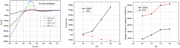
Figure 8. Simulated N curve for Cell ratios; 0.5 → 2 and performance parameters SINM, WTI, SVNM and WTV.
Download figure:
Standard image High-resolution image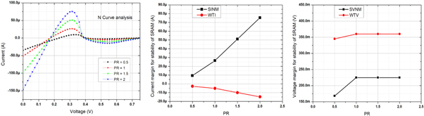
Figure 9. Simulated N curve for Pull up ratios; 0.5 → 2 and performance parameters SINM, WTI, SVNM and WTV.
Download figure:
Standard image High-resolution image
In this paper, the charge plasma based doping less TFET (CP-DLTFET) based 6T SRAM cell [22 ] are reported to analyze the cell performance in terms of SNM, SINM, WTV, WTI, SNMP and WTP for various values for cell ratio (CR) and pull up ratio (PR). It is observed from the table 4, that the maximum value of SNPM (16 μW) and SNPM (6.38 μW) are reported for CR = PR = 2 respectively; the minimum value of WTP (0.096 μW) and WTP (0.242 μW) are reported for CR = PR = 0.5 respectively. From the table it also shows that, the decrement in the write ability with increment in the cell ratio (CR), because of degraded performance of WTV with respect to cell ratio. Table 4 indicates SVNM increases with pull-up ratio but, after 1.5 pull up ratio, SVNM does not show significant variations. WTI almost not affected by cell ratio and shows the negligible effect on WTI due to change in pull-up ratio. Here the read stability again shows good agreement with CR and PR but on other hand the SRAM is losing the write ability with CR and PR.
Table 4. Comparing the read stability and write ability of 6T SRAM cell based on Si Double gate TFET (DGTFET) and charge plasma based doping less TFET (CP-DLTFET)*.
| CR | SVNM (V) | SVNM* (V) [22 ] | WTV (V) | WTV* (V) [22] | SINM (μA) | SINM* (μA) [22] | WTI (μA) | WTI* (μA) [22] | SNPM (μW) | ∣WTP∣ (μW) | SNPM* (μW) [22] | ∣WTP∣* (μW) [22] |
|---|---|---|---|---|---|---|---|---|---|---|---|---|
| 0.5 | 0.095 | 0.26 | 0.27 | 0.48 | 2.55 | 20.00 | −1.37 | 0.2 | 0.24225 | 0.3699 | 5.2 | 0.096 |
| 1 | 0.126 | 0.29 | 0.285 | 0.5 | 1.20 | 36.00 | −4.70 | 1 | 0.1512 | 1.3395 | 10.44 | 0.5 |
| 1.5 | 0.165 | 0.32 | 0.35 | 0.5 | 47.00 | 46.00 | −13.60 | 0.2 | 7.755 | 4.76 | 14.72 | 0.1 |
| 2 | 0.17 | 0.32 | 0.36 | 0.52 | 85.00 | 50.00 | −16.50 | −1.75 | 14.45 | 5.94 | 16 | 0.91 |
| PR | SVNM (V) | SVNM* (V) [22 ] | WTV (V) | WTV* (V) [22] | SINM (μA) | SINM* (μA) [22] | WTI (μA) | WTI (μA) | SNPM (μW) | ∣WTP∣ (μW) | SNPM* (μW) [22] | ∣WTP∣* (μW) [22] |
| 0.5 | 0.17 | 0.24 | 0.35 | 0.48 | 9.40 | 20.00 | −2.72 | −0.8 | 1.58202 | 0.9384 | 4.8 | 0.384 |
| 1 | 0.23 | 0.25 | 0.36 | 0.49 | 26.50 | 21.00 | −5.12 | −1 | 5.9625 | 1.8432 | 5.25 | 0 0.49 |
| 1.5 | 0.23 | 0.285 | 0.36 | 0.5 | 51.00 | 21.00 | −9.96 | −1.8 | 11.475 | 3.5856 | 5.985 | 0.9 |
| 2 | 0.23 | 0.29 | 0.36 | 0.52 | 75.40 | 22.00 | −14.80 | −2 | 16.965 | 5.328 | 6.38 | 1.04 |
There are various methods and ways mentioned in literature to analyze the performance of SRAM cell in terms of Read margin and Write margin. Various definitions can be used to analyze the write ability of SRAM cell in terms of SWNM, WLM, CWLM and BLM and these are also reexamined by analyzing the dependence of the Write margin (WM) on the SRAM cell transistor threshold voltages (Vth's) in order to find a preferable definition [40]. The performance of SRAM cell is also analyzed as a function device parameters and supply voltage by developing the explicit expressions for static-noise margin (SNM: RSNM and HSNM). These expressions are also useful in predicting the effect of parameter changes on the stability as well as in optimizing the design of SRAM cells [41].
Here in this paper we have performed only the N curve simulations to carry out analysis on write ability and read stability of SRAM cell for various CR and PR.
6. Conclusion
Look up table based verilog-A model has shown promising results in order to analyze the dc and transient performance of DGTFETs based circuits. The propagation delay across the chain of inverters which is driving the large capacitance as a load can be minimized by choosing proper value of inverter stage size ratio (b); which is reported as, b = 3 in the simulation results. Band to band tunneling in DGTFET is responsible for charge coupling between the source and drain, hence causing partial self loading which is consistent with the calculated value of processing parameter (γ = 0.295). Simulation results show that the N curve method can be one of the best ways to study and analyze the performance of 6 T SRAM cell. The read stability of 6 T SRAM cell shows good agreement with cell ratio and pull up ratio but on other hand, the 6 T SRAM is losing the write ability with the cell ratio and pull up ratio. Therefore it s needed to choose proper range of cell ratio and pull up ratio in order to optimize the read stability and write ability of 6 T SRAM cell.
Acknowledgments
I would like to express my sincere gratitude to Dr Shiromani Balmukund Rahi (Ph.D Scholar, Department of Electrical Engineering, Indian Institute of Technology Kanpur) for his continuous feedback regarding the suggestions and corrections to frame this research paper.