
Abstract
Transfer printing based on switchable adhesive that heterogeneously integrates materials is essential to develop novel electronic systems, such as flexible electronics and micro LED displays. Here, we report a robust design of a thermal actuated switchable dry adhesive, which features a stiff sphere embedded in a thermally responsive shape memory polymer (SMP) substrate and encapsulated by an elastomeric membrane. This construct bypasses the unfavorable micro- and nano-fabrication processes and yields an adhesion switchability of over 1000 by combining the peel-rate dependent effect of the elastomeric membrane and the thermal actuation of the sub-surface embedded stiff sphere. Experimental and numerical studies reveal the underlying thermal actuated mechanism and provide insights into the design and operation of the switchable adhesive. Demonstrations of this concept in stamps for transfer printing of fragile objects, such as silicon wafers, silicon chips, and inorganic micro-LED chips, onto challenging non-adhesive surfaces illustrate its potential in heterogeneous material integration applications, such as flexible electronics manufacturing and deterministic assembly.
Export citation and abstract BibTeX RIS

Original content from this work may be used under the terms of the Creative Commons Attribution 3.0 license. Any further distribution of this work must maintain attribution to the author(s) and the title of the work, journal citation and DOI.
1. Introduction
Transfer printing is an emerging material assembly technique, which utilizes an elastomeric stamp with switchable adhesion to transfer inks (i.e. objects to be transferred) from their donor substrate onto a receiving substrate. It is essential to develop existing and envisioned systems such as stretchable electronics [1–13] and flexible electronics [14–24]. The transfer yield of transfer printing critically depends on the ability of a switchable adhesive to change from a strong state for pick-up to a weak state for printing. The chemical adhesive that exploits surface chemistry to regulate the interfacial adhesion via external stimuli, such as water, heat, or UV light is reliable for transfer printing [25–29], but the lack of reversibility greatly limits its broad utility. To ensure efficient transfer printing, a switchable dry adhesive with high reversibility is desired. Various strategies based on structure designs or smart materials have been proposed and provide promising solutions to meet the above requirement. Typical examples of switchable adhesive based on structure designs are the gecko-inspired dry adhesive with fibrillar surface assisted by retraction angle or lateral movement [30–32], the aphid-inspired dry adhesive with surface topography modulated by external stimuli (e.g. heating, magnetic field, or pneumatic pressure) [33–37], and the octopus-inspired dry adhesive with cavity pressure controlled by external stimuli [38, 39]. These bio-inspired switchable dry adhesives are very valuable despite the required delicate designs and relatively complex fabrication process of surface micro-structures (e.g. photolithography, wet etching). Smart materials especially shape memory polymers (SMPs) have been widely used to develop switchable adhesives due to their unique properties of memorizing temporary shapes and fully recovering to their original shapes upon external stimuli (e.g. heat, light) [40–44]. For example, Xie et al adopted a simple bilayer structure consisting of a thin adhesive layer and an SMP layer to achieve a self-peeling switchable and reversible dry adhesive [45]. Linghu et al utilized a simple, heat-responsive SMP block to manipulate multiscaled, arbitrarily shaped objects [46]. To further enhance the performance of SMP-enabled dry adhesives, surface micro-structures (e.g. micro-posts, micro-pyramids) were introduced to combine the superior properties of structure designs and the multi-functionality to external stimuli of smart materials [47–54].
Here, we report an alternative design of a thermal actuated switchable dry adhesive with high reversibility, in which localized regions of an elastomer/SMP composite stamp are controlled in a fashion similar to that of a balloon. The switchable adhesive features a stiff sphere embedded in a thermal responsive SMP substrate and encapsulated by an elastomeric membrane. This construct bypasses unfavorable micro- and nano-fabrication processes via molding and pressing processes and yields an attractive level of switchable adhesion through a combination of the peel-rate dependent effects of an elastomeric membrane and the thermal actuation of a sub-surface embedded stiff sphere. Experimental and numerical studies reveal the underlying thermal actuated mechanism and provide insights into the design and operation of the switchable adhesive. Demonstrations of this concept in the form of stamps capable of transfer printing fragile objects, such as silicon wafers, silicon chips, and inorganic micro-LED chips onto challenging non-adhesive surfaces in deterministic ways illustrate the robust capabilities of thermal actuated switchable adhesives and their immense potential in heterogeneous material integration applications.
2. Results and discussion
Figure 1 schematically shows the transfer printing process enabled by the thermal actuated switchable adhesive, or stamp. Here, the stamp has a stiff sphere embedded in a thermal responsive SMP substrate and encapsulated by an elastomeric membrane, as illustrated in figure 1(a). The embedding of the stiff sphere was achieved by pressing it into the heated SMP, which was cooled to fix the temporary shape so the membrane remained flat to maximize the areal interfacial contact and the corresponding adhesive force. This flat state is referred as the 'adhesion on state.' The transfer printing began by moving the stamp above a donor substrate (figure 1(a)). The stamp was then brought into contact with the ink (figure 1(b)). The stamp was quickly retracted, picking up the ink from the donor substrate (figure 1(c)). The inked stamp was then brought into contact with the receiving substrate. The stamp was heated, causing the SMP to return to its original shape, which pushed the stiff sphere out, creating a bulge in the membrane and reducing the adhesive force (figure 1(d)). This bulge state is referred as the 'adhesion off state.' The slow retraction of the stamp left the ink on the receiving substrate (figure 1(e)). The stamp was heated, pressed to a flat state, and cooled to maintain the adhesion on state for the next transfer printing cycle (figure 1(f)).

Figure 1. Schematic illustration of the transfer printing process enabled by a thermal actuated switchable dry adhesive (or called stamp). (a) The stamp is moved above the donor. (b) The stamp is in contact with the ink. (c) The ink is quickly picked up by the stamp. (d) The inked stamp is moved above the receiver followed by heating, which recovers the permanent shape of SMP substrate to bulge the elastomeric membrane. (e) The ink is printed onto the receiver after the stamp is removed slowly. (f) The heated stamp is pressed onto a flat substrate and then cooled down to fix the flat state at room temperature for the next transfer printing cycle.
Download figure:
Standard image High-resolution imageThe thermal actuated switchable adhesive features three critical components: (a) a thermal responsive SMP that serves as the substrate to embed stiff spheres; (b) stiff spheres embedded in the SMP substrate that enable switchable adhesion; and (c) a thin elastomeric membrane that encapsulates the stiff spheres and SMP substrate and serves as the interface between the stamp and ink. Figure 2(a) shows an image of a representative thermal actuated stamp consisting of a thermal responsive epoxy SMP substrate (30 mm × 30 mm × 8.5 mm), a steel ball (5 mm in diameter), and a polydimethylsiloxane (PDMS, Dow Corning Sylgard 184 with 10:1 monomer: cross-linking agent) membrane (30 mm × 30 mm × 1.3 mm). The stamp provides thermal actuated switchable adhesion by controlling the bulge configuration of the steel ball. The non-bulging configuration corresponds to the adhesion on state, while the bulging configuration corresponds to the adhesion off state. Figure 2(b) shows the storage modulus and loss factor of epoxy SMP as functions of temperature. The glass transition temperature of SMP is around 45 °C. To characterize the performance of thermal actuated switchable adhesive, vertical pull tests were carried out under various preloads and retraction speeds for a stamp/glass interface. The measurement setup (figures S1(a) and (b) (available online at stacks.iop.org/IJEM/3/035103/mmedia)) consists of a material testing system, a manual tilt stage, and a thermal stage. The pull test procedure is schematically shown in figure S1(c). The glass slide approached the stamp at a speed of 100 μm s−1. After applying a preload for 20 s, we pulled the glass slide at a specific speed until it separated from the stamp. The pull-off force is given by the maximum pull force from the force-displacement curve (figure 2(c)). The adhesion strength can then be obtained by distributing the pull-off force over the interfacial contact area.

Figure 2. The thermal actuated switchable adhesive and its adhesion characteristics. (a) Photography of the thermal actuated stamp with reversible adhesion states. (b) Storage modulus and loss factor of SMP as functions of temperature. (c) Typical force-displacement curve of pull test. Measured adhesion strengths of the stamp/glass interface as functions of preload (d) and retraction speed (e), respectively. Insets: adhesion switchability. (f) Reversibility and repeatability tests of adhesion measurements.
Download figure:
Standard image High-resolution imageFigure 2(d) shows the measured adhesion strengths of the stamp/glass interface under two adhesion states as functions of preload at a fixed retraction speed of 100 μm s−1. The adhesion strength under the adhesion on state had a positive correlation with the preload before reaching a plateau. In other words, the adhesion strength increased with the preload until the preload exceeded a critical load (around 10 N in this case). The adhesion strength under the adhesion off state was much lower than that under the adhesion on state, and it depended on the preload (see figure S2(a)). The adhesion switchability (i.e. the maximum adhesion strength over the minimum adhesion strength) increased with the preload and reached above 300 in experiments under a fixed retraction speed of 100 μm s−1 (see inset in figure 2(d)). The influence of retraction speed on adhesion strength is shown in figure 2(e) with a fixed preload of 1 N. As expected, the adhesion strength is rate-dependent due to the viscosity effect of the PDMS membrane [55]. The adhesion strength had a positive correlation with the retraction speed regardless of whether the stamp is in adhesion on or off states (figure S2(b)). The maximum adhesion switchability under a fixed preload of 1 N reached 1000 (see inset in figure 2(e)), which is superior to most existing stamp designs [48]. Increased preload can further enhance the adhesion switchability. However, a larger preload is not preferred for fragile inks, such as ultra-thin silicon wafers. Figure 2(f) shows the reversibility and repeatability of the thermal actuated adhesive under a preload of 10 N and a retraction speed of 100 μm s−1. Due to the SMP's high shape fixation ratio (greater than 99.8%), no visible blistering of the PDMS layer was observed in experiments after the planishing step. The high and low adhesion strengths had negligible changes during the cycle test, which indicates that the thermal actuated adhesive has desirable adhesion performance.
To enhance the operation of the thermal actuated stamp, a flexible printed circuit (FPC) was incorporated into the stamp and served as the heating source for actuation. Figure 3(a) shows a tilted, magnified view of the FPC-enabled thermal actuated stamp. The FPC heater was integrated inside the SMP substrate and under the embedded steel ball. Figure 3(b) shows a photograph of the FPC enabled thermal actuated stamp (40 mm in diameter). The thicknesses of the SMP and PDMS were 20 mm and 1.3 mm, respectively. The FPC heater (figure S3(a)) was 35 mm in diameter and 1 mm in line width with the hollow part designed to reduce unfavorable compression from the steel ball (5 mm in diameter). The vertical distance from the FPC heater to the top surface of the SMP substrate was 8 mm. To prove that the FPC heater could provide enough heating to the system, we put a bare heater on an SMP substrate and monitored the surface temperature using an infrared camera (C400M, Guide Sensmart Tech Co., Ltd) when the heater was on, as shown in figures S3(b) and S3(c). Figure 3(c) shows the surface temperature as a function of time under various input currents. As expected, the temperature increased as the input current increased, and the temperature reached a stable state within 5 s. An input current of 2.0 A or larger may be enough to induce phase change of SMP and switch the adhesion state. The input current was set at 3.0 A in these experiments, considering that the higher the temperature, the faster the adhesion switching speed.

Figure 3. The FPC-enabled thermal actuated stamp and its application in transfer printing. (a) The magnified view of the FPC-enabled thermal actuated stamp illustrating various components. (b) Photography of the thermal actuated dry adhesive stamp (diameter: 40 mm), which includes SMP substrate (thickness: 20 mm), FPC heater (thickness of Cu layer: 35 μm, thickness of polyimide layer: 200 μm), steel ball (diameter: 5 mm) and PDMS membrane (thickness: 1.3 mm). (c) The surface temperature of the bare FPC heater on the SMP substrate as a function of time under various input currents of 1 A, 2 A, and 3 A. (d) Photography of side views of the FPC-enabled thermal actuated stamp under two adhesion states. (e) FEA simulation visualizing the principal strain of the PDMS membrane under the adhesion off state. (f) Snapshots of the transfer printing of a silicon wafer in a non-contact mode. Inset: infrared thermography of the stamp after transfer printing process.
Download figure:
Standard image High-resolution imageFigure 3(d) shows the side views of the FPC-enabled thermal actuated stamp under two adhesion states. Obvious flat and bulging configurations were observed for the adhesion on and off states, respectively. An axisymmetric finite element model was also established to assess the deformations of the PDMS membrane and SMP substrate under the adhesion off state. The bugle height was set at 3 mm, which was measured in experiments. The maximum principal strains in the PDMS membrane and SMP substrate reached 24.75% (figure 3(e)) and 16.81% (figure S4), which are much smaller than their fracture strains of over 100% [40, 56]. To demonstrate the capabilities of the FPC-enabled thermal actuated stamp, the transfer printing of a 4-inch silicon wafer in a non-contact mode is demonstrated in figure 3(f). The wafer was placed on a piece of clean glass and then picked up by the stamp at room temperature with the heater off. After heating for around 35 s, the steel ball bugled and pushed the wafer out onto the glass. The red dotted frame shows the temperature distribution of the stamp after the completed transfer printing process. The maximum temperature was 77 °C, which indicates that no thermal damage was induced in the system. It should be noted that the FPC-enabled thermal actuated stamp is also applicable for transfer printing in a contact mode (i.e. the stamp should come in contact with the receiving substrate during printing) since contact transfer printing places less stringent requirements on switchable adhesives.
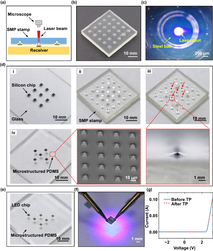
Another attractive feature of the thermal actuated stamp is that the steel balls can be individually actuated, thus providing the potential for programmable transfer printing. Figure 4(a) shows a schematic of the programmable transfer printing platform based on a stamp with multiple thermal responsive regions with the aid of laser heating. The platform consists of a laser-generation system, a displacement control system, and a microscope monitoring system. As shown in figure 4(b), we fabricated the stamp using much smaller steel balls with diameters of 1 mm (arranged in a 5 × 5 array with a spacing of 7 mm) to be compatible with the laser spot size (300 μm in diameter). The PDMS membrane thickness was 0.5 mm. The laser beam had a wavelength of 808 nm, a duration time of 1 s, and an input power of 1 W. Figure 4(c) shows the microscopy of the laser-heated steel ball. The laser spot size was comparable to diameter of the steel ball such that the laser heating rapidly dissipated within the steel ball to ensure a quick thermal response within the system. To further enhance the printing speed, the size of the steel ball should be decreased to match the laser spot size.
Figure 4. Programmable transfer printing enabled by the thermal actuated stamp with the aid of laser heating. (a) Schematic illustration of programmable transfer printing platform. (b) Photography of the thermal actuated stamp for programmable transfer printing (thickness of SMP layer: 5 mm, thickness of PDMS membrane: 0.5 mm, diameter of steel ball: 1 mm, Spacing of steel ball: 7 mm). (c) Microscopic photography of the steel ball selectively heated by the laser beam. (d) Programmable transfer printing of silicon chips to a microstructured PDMS substrate. (i) An array of silicon chip is placed on a flat glass. (ii) The silicon chips are picked up by the thermal actuation stamp. (iii) A pattern of the steel balls is heated by the laser beam and the unheated silicon chips remain on the stamp. (iv) The heated silicon chips are printed onto the microstructured PDMS substrate (e) Programmable printing of LED chips with a triangular pattern onto a microstructured PDMS substrate (f) The printed LED chip is lighted by a multimeter. (g) Voltage-current curves of the LED chip before and after transfer printing.
Download figure:
Standard image High-resolution image
The unusual capabilities of the thermal actuated stamp are demonstrated by programmable transfer printing of silicon chips (2 mm × 2 mm × 530 μm) and LED chips (2 mm × 2 mm × 150 μm) onto challenging non-adhesive surfaces, such as a microstructured PDMS substrate, which are not easily accessible via other adhesive schemes. As a demonstration, a 3 × 3 array of single polished silicon chips were placed on the glass surface (figure 4(d)(i)). The silicon chips were then picked up by the thermal actuated stamp (figure 4(d)(ii)) and selectively heated by the laser beam (figure 4(d)(iii)). The heated steel balls are marked by red arrows, which clearly indicates that these heated steel balls bulge out from the SMP substrate. These selected silicon chips were transfer printed onto the microstructured PDMS substrate with micro-pyramids (10 μm × 10 μm × 6.6 μm) (figure 4(d)(iv)). The unheated silicon chips remained on the stamp. Figure 4(e) shows the programmable transfer printing of LED chips onto the microstructured PDMS substrate. The optical and scanning electron microscope images of the LED chip on the microstructured PDMS substrate are shown in figure S5. The LED chip was lit by a multimeter after transfer printing, as shown in figure 4(f). Figure 4(g) shows the voltage-current curves of the LED chip before and after transfer printing, which indicates that its performance is not influenced by the transfer printing process. The microstructured PDMS substrate with micro-pyramids represents a challenging receiver with weak adhesion. These demonstrations illustrate the great potential of the thermal actuated stamp for deterministic assembly as well as heterogeneous material integration applications.
It should be noted that the thermal actuated switchable dry adhesive is limited by its cycle time due to the heating and cooling, which limits the transfer printing. However, this limit depends on various parameters such as the ink size and heating method. For transfer printing of objects with large size, such as a 4-inch silicon wafer, via FPC global heating, the cycle time is about 1 min. The cycle time is about 10 s for transfer printing small objects, such as a 2 mm LED chip, via local laser heating. Future work should pay focus on reducing the limit of cycle time by adopting rapid heating and cooling strategies. Moreover, transfer printing through laser heating induces a thermal effect on neighboring objects, which may yield a minimum distance between objects without thermal effects. This minimum distance depends on several factors, such as the size of the ball, the diameter of laser spot, and the laser heating duration time, which require further exploration.
3. Fabrication and testing
3.1. Fabrication of the thermal actuated stamp for pull tests (see figure S6)
A thin-walled aluminum pan is used as the mold for curing epoxy SMP, which is composed of an epoxy monomer E44 (China Feicheng Deyuan Chemical Corp.) and a curing agent Jeffamine D230 (Sigma-Aldrich). The liquid mixture (weight ratio of 81:46) was cured in an oven at 100 °C and 130 °C for 1 h, respectively. Then a steel ball (diameter: 5 mm) was completely pressed into the heated SMP (thickness: 8.5 mm) until the SMP cooled down. Afterward, a room temperature curing silicone (type-705) was spin-coated on the surface of the SMP at a speed of 2000 rpm, which bonded the SMP substrate and PDMS membrane (Sylgard 184, Dow Corning). The thickness of the thin silicone layer was 45 μm. To prepare the PDMS membrane (thickness: 1.3 mm), a spot of liquid PDMS mixture (10:1 base to crossing-linking agent ratio) was poured into a small thin-walled aluminum pan, degassed in a vacuum chamber for 15 min, and then cured in an oven at 75 °C for 4 h. Both the silicone-coated SMP and PDMS membrane were exposed in a plasma cleaner for 45 s before forming strong chemical bonds. Finally, the thermal actuated stamp was cut into a block with an in-plane size of 30 mm × 30 mm.
3.2. Pull tests
A clean glass slide (50 mm × 50 mm × 1.3 mm) was attached to a two-axes manual tilt stage with the purpose of forming a leveling contact with the SMP stamp. Then the tilt stage and the force sensor of the materials testing system (Model 5944, Instron) were fitted together. The resolution of the force sensor was 2 mN. The thermal actuated stamp was attached to the thermal stage. During the pull test, the glass slide first approached and contacted the stamp at a fixed speed of 100 μm s−1 under a given preload and then retracted at a given speed after relaxing for 20 s. To test the pull-off force in the adhesion off state, the heating plate was turned on with a setting temperature of 120 °C to bulge the steel ball out of the SMP substrate.
3.3. Fabrication of the FPC-enabled thermal actuated stamp (see figure S7)
An aluminum mold was fabricated using a numerical-controlled machine tool. Then the liquid PDMS mixture (10:1 base to crossing-linking agent ratio) was poured into the aluminum mold and degassed in a vacuum chamber for 30 min. Next, the PDMS was cured in an oven at 75 °C for 4 h. The liquid SMP mixture was poured into the PDMS mold, filling about 1/3 of the cavity volume. The mold was cured again at 100 °C for 1 h. Then, a piece of the FPC heater was carefully attached to the heated SMP. The rest of cavity volume was filled with liquid SMP mixture followed by 1 h curing and post-curing at 100 °C and 130 °C, respectively. After this, the room temperature curing silicone (type-705) was spin-coated on the surface of the SMP at a speed of 2000 rpm. The thickness of the thin silicone layer was 45 μm. The remaining procedures are same as those described in section 3.1.
3.4. Mechanical modeling and FEA
Two axisymmetric finite element models were established to study the deformations of the PDMS membrane and SMP substrate (adhesion off state) in ABAQUS, respectively. The diameter of the steel ball was 5 mm. The diameter and thickness of the PDMS were 15 mm and 1.3 mm and 40 mm and 8.5 mm for the SMP substrate. Considering that the steel ball is much stiffer than the PDMS and heated SMP, the steel ball was set as rigid body in finite element analysis (FEA). The Young's modulus and Poisson's ratio were 1 MPa and 0.48 for PDMS, and 0.9 MPa and 0.38 for the heated SMP. In the PDMS model, a longitudinal displacement of 3 mm was applied to the steel ball while keeping the edge of the PDMS membrane fixed (figure 3(e)). In the SMP model, a longitudinal displacement of 2 mm was applied to the steel ball while keeping the bottom of the SMP fixed (figure S4).
3.5. Transfer printing of silicon wafer
A home-made acrylic clamp was assembled with the materials testing system (Model 5944, Instron). Then the FPC-enabled thermal actuated stamp was fixed to a glass slide (50 mm × 50 mm × 1.3 mm) by double-side tape. Next, the glass slide was inserted into the home-made acrylic clamp, which was connected to a direct-current (DC) power source (power off). After completing the setup, the stamp approached and contacted a 4-inch silicon wafer (thickness: 450 μm) at a fixed speed of 100 μm s−1. A 10 N preload was applied to ensure intimate contact between the stamp and the wafer. After a relaxation period of 10 s, the clamp retracted at a fixed speed of 100 μm s−1 to pick up the wafer from the glass substrate. The power was turned on with a current of 3 A. The steel ball gradually bulged out in 35 s and pushed the wafer onto the glass substrate.
3.6. Fabrication of a laser actuated stamp
A thin-walled aluminum pan was used as the mold for curing the epoxy SMP in an oven at 100 °C and 130 °C for 1 h. Then a 5 × 5 array of steel balls (diameter: 1 mm, spacing: 7 mm) were completely pressed into the heated SMP (thickness: 5 mm) using a piece of iron plate until the SMP cooled down. Next, the room temperature curing silicone was spin-coated on the surface of the SMP at a speed of 2000 rpm. A spot of liquid PDMS (10:1 base to crossing-linking agent ratio) mixture was dropped on a clean circular glass substrate followed by spin-coating at speed of 500 rpm. Then the glass substrate was placed in an oven at 75 °C for 4 h. The PDMS membrane (thickness: 0.5 mm) was cut into an in-plane size of 40 mm × 40 mm. Both of the silicone-coated SMP and PDMS membrane were exposed in a plasma cleaner for 45 s before forming strong chemical bonds. Finally, the laser actuated stamp was cut into a block with an in-plane size of 40 mm × 40 mm.
3.7. Programmable transfer printing of silicon chips and LED chips
At first, the laser actuated stamp manually picked up the array of silicon chips or LED chips (NSS-D7676A1, San'an Optoelectronics CO., Ltd) from the glass substrate. By using a laser-generation system (FC-W-808 nm-10 W, Changchun New Industries Optoelectronics Tech. Co., Ltd) [28, 33, 46], the chips were printed onto the microstructured PDMS substrate in a defined pattern with a power of 1 W. The laser beam used here had a wavelength of 808 nm and a duration time of 1 s. The beam profile was round and the focal length of the lens was 40 mm.
4. Conclusion
In this paper, we report a thermal actuated switchable dry adhesive, which features a stiff sphere embedded in a thermally responsive SMP substrate and encapsulated by an elastomeric membrane. The adhesive combines the peel-rate dependent effects of an elastomeric membrane and the thermal actuation of a sub-surface embedded stiff sphere to offer an adhesion switchability of over 1000, which far surpasses most existing dry adhesive schemes. Moreover, the adhesion on state works at room temperature, which prevents the high thermal stress induced in other SMP-based dry adhesives. Demonstration of this concept in an FPC-enabled thermal actuated stamp for transfer printing a fragile silicon wafer in a non-contact mode illustrates its robust capability for heterogeneous material integration. With the aid of laser heating, the proposed adhesive enables programmable transfer printing of fragile silicon chips and LED chips onto challenging receivers, such as microstructured PDMS substrates with micro-pyramids, which is not easily performed via other transfer printing schemes. Thus, the proposed thermal actuated switchable dry adhesive shows enormous potential in flexible electronics manufacturing.
Acknowledgments
The authors acknowledge financial support from the National Natural Science Foundation of China (Grant Nos. 11872331 and U20A6001) and the Zhejiang University K P Chao's High Technology Development Foundation.