
Abstract
This article presents the three paradigms of manufacturing advancement: Manufacturing I, craft-based manufacturing by hand, as in the Stone, Bronze, and Iron Ages, in which manufacturing precision was at the millimeter scale; Manufacturing II, precision-controllable manufacturing using machinery whereby the scales of material removal, migration, and addition were reduced from millimeters to micrometers and even nanometers; and Manufacturing III, manufacturing objectives and processes are directly focused on atoms, spanning the macro through the micro- to the nanoscale, whereby manufacturing is based on removal, migration, and addition at the atomic scale, namely, atomic and close-to-atomic scale manufacturing (ACSM). A typical characteristic of ACSM is that energy directly impacts the atom to be removed, migrated, and added. ACSM, as the next generation of manufacturing technology, will be employed to build atomic-scale features for required functions and performance with the capacity of mass production. It will be the leading development trend in manufacturing technology and will play a significant role in the manufacture of high-end components and future products.
Export citation and abstract BibTeX RIS

Original content from this work may be used under the terms of the Creative Commons Attribution 3.0 license. Any further distribution of this work must maintain attribution to the author(s) and the title of the work, journal citation and DOI.
1. Background and significance
1.1. Historical development of manufacturing
Throughout history, no revolution was possible without technical innovation; and the advancement of developed countries is inseparable from industrial transformation. Manufacturing is the core of industrial production, while the products that are made meet the material and spiritual needs of humans. Manufacturing is defined as the entire process of making products from raw materials that satisfy the users' demands, and the key is to obtain the required performance and fulfill the usage requirement of the products. Significant progress can be made only if people grasp the law of manufacturing technology development and take the lead in future development trends. History of mankind has been accompanied by the development of manufacturing, while the history of manufacturing consists of the following three main phases, according to its precision and inherent law of development as shown in figure 1 [1].
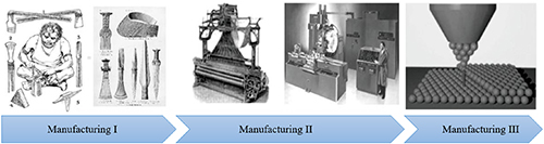
Figure 1. The three phases of manufacturing development.
Download figure:
Standard image High-resolution imageManufacturing I: Craft-based manufacturing by hand, as in the Stone, Bronze, and Iron Ages, in which manufacturing precision is at the millimeter scale.
As early as the Stone Age, mankind made living supplies with stone tools [2, 3]. By the Bronze and Iron Ages, people began to develop tools for mining, smelting, and casting to meet the demands of the agricultural economy and to make textile machinery, hydraulic machinery, and transport vehicles, etc [4, 5]. People have been crafting tools and other products in primitive workshops for a long period of time. Gradually, the means of production was conventionalized, and simple division of labor was formed. This was the first development phase of manufacturing technology, i.e. Manufacturing I, which was a handcraft art. The manufacturing precision was determined by experience and was at the millimeter scale. Mass and repeatable production was not possible in this 'manufacturing' phase.
Manufacturing II: Precision-controllable manufacturing using machinery whereby the material removal, migration, and addition scales were reduced from millimeters to micrometers and even nanometers.
Manufacturing technology advanced continually with the progress of industrialization. Basic manufacturing theory was based on classical mechanics, formed progressively, and improved from time to time. The minimum material to be removed in contemporary machining has been reduced from millimeters to micrometers and even nanometers [6]. In the late 18th century, the industrial revolution, represented by the successful development of the Watt steam engine technology and tooling machines, propelled machinery to replace manual labor. The combination of mechanical technology and steam engines spawned modern manufacturing methods, which drove social transformation from agricultural and handcraft to industrialization and mechanically driven manufacturing.
The saying, 'The sun never sets on the British Empire,' was formed because the UK pioneered this industrial revolution [7]; and it quickly developed in Europe at the same time. The appearance of the first modern production line in Cincinnati's slaughterhouse in 1870 marked the introduction of automatic technology; and another great change in industry was achieved by production models that used electrification, assembly lines, and mass production. America soared to a superpower as it seized the opportunities that manifested during this period of time [8].
The programmable logic controller was invented in the 1960s, and the mechanical equipment used by information technology and automation control stood in the limelight of industrial production. Asian countries, e.g. Japan and South Korea, recovered quickly following World War II and joined the ranks of developed countries [9]. Today, industrial nations are exploring 'Industry 4.0,' which is mainly focused on the creation of 'cyber-physical systems' [10]. The real world is closely connected by a sensor network, which acquires and analyzes data related to design, development, and manufacturing and hence realizes the intelligent management and production for the life cycle of products and facilities. In general, although mankind has experienced several industrial revolutions in this phase, the fundamental theory of manufacturing and production is based on classical theories. They are collectively referred to as 'Manufacturing II.'
Manufacturing III: Manufacturing objectives and processes directly focused on atoms, spanning the macro- through the micro- to the nanoscale whereby manufacturing is based on removal, migration, and addition at the atomic scale, namely, atomic and close-to-atomic scale manufacturing
One of the main elements of manufacturing is machining. When machining is scaled down from the micro/nano to the atomic level, the phenomena of material removal, migration, and addition at the atomic scale can no longer be explained by classical theories. Contemporary manufacturing technology that is characterized by classical theories, i.e. macro statistical analysis and engineering experiences, will be pushed forward to the next generation of manufacturing technology, which will be multidisciplinary and based on quantum theory. This type of atomic and close-to-atomic scale manufacturing (ACSM) is known as 'Manufacturing III' [11–14]. The essential attribute of Manufacturing III is distinguished from Manufacturing II by its theoretical fundamentals, in which quantum theory dominates [14, 15].
The presented differentiator between Manufacturing III and Manufacturing II has seemed the scaling difference, whereby the manufacturing precision is down to the atomic scale. However, the fundamental difference is that Manufacturing III will be built on quantum theory. Classifying a system if it is governed by classic theory or quantum theory is determined by the relationship between the de Broglie Wavelength and the system scale or the distance between the particles. If the de Broglie Wavelength is larger than the system scale or the distance between the particles, it is recognized as a quantum system. It is not sufficient if we judge a classic or quantum system by only considering the system scale. In short, there will be a process from quantitative to qualitative changes for manufacturing technology.
Manufacturing III will not replace Manufacturing I and II, but the three paradigms will exist in parallel.
1.2. Significant needs of development in science and technology
Manufacturing is the foundation of social, economic, and productive force development. Currently, there appears to be an understanding that everything is possible once people have microchips, networks, and software. Admittedly, they are important. However, microchips need to be manufactured, while high-end microchips rely on high-end manufacturing, in which high-precision lithography is the core. Microchips, networks, and software only deal with the processing (including computing), storage, and transmission of information (including data). The acquisition of information depends on sensors and various sensing devices. Without precision sensors, achieving artificial intelligence, precision navigation, and other high-end products is an empty promise. Precision actuators are also required to perform precise motion.
The further development of the current manufacturing fundamentals and technologies is facing great difficulties, while great challenges and insurmountable gaps have been brought to existing manufacturing methods that regard processing objects as continuous materials. These challenges include:
- Whether distributed nodes can continually increase density on microchips according to Moore's law.
- Development of new materials is restricted by the existing manufacturing capabilities and, consequently, restricted by the design freedom.
- The current microsystems manufacturing platform is gradually showing its insufficiency, as it cannot meet the needs of disruptive upgrade and iteration with complexification and intellectualization.
High-precision manufacturing plays a key role in the development of future technologies with high productivity. Take chips for example. To achieve high precision, manufacturing and motion control technologies are required at the nanometer level, even at the atomic and close-to-atomic scale. The advancement of science and technology has become more and more dependent on multidisciplinary development in this era of rapid change. ACSM is the cutting edge manufacturing technology in which energy is directly applied to atoms. Specific function and performance is implemented by creating atomic-scale structures, and mass production will be realized to meet the demands. It is the leading development trend of the next generation of manufacturing technology for breaking the aforementioned bottlenecks and is of great significance to future technological advancement and high-end component manufacturing [16].
Whether the next generation of core elements will be phonics chips, quantum chips, or other revolutionary components that are not yet foreseen, the need for future manufacturing technologies is inevitable once a product is launched. As the representative of the next generation of manufacturing technology, the launching, planning, and implementation of ACSM will play an important role in supporting worldwide development in science and technology and will help each individual country to seize the opportunity of developing their own manufacturing capability.
1.3. Research status
ACSM is a new field, some researchers and research organizations have already started to carry out investigations. The Defense Advanced Research Projects Agency (DARPA) in the U.S. launched the Atoms-to-Product (A2P) research program in 2014, aimed at developing methods of manufacturing by assembly that enable manufactured large-scale materials, components, and systems to retain the properties of nanomaterials [17, 18]. To solve the problem of reliability caused by the long-term interaction between electronic products and the environment, research was conducted on 'from atom to product reliability', targeted at reducing the impact of the interaction on system reliability at the atomic level [19].
In 2016, researchers from the Chinese Academy of Engineering Physics elaborated on the significance of atomic manufacturing by combining it with the constrained integrated microsystem [20]. In 2018, scientists from the University of Alberta explored how to apply machine learning in atomic manufacturing, providing solutions to promote the development of atomic-scale, low-power electronics, which is expected to make their mass production possible [21]. In 2019, Huawei established the Strategic Research Institute to officially designate atomic manufacturing as one of its key research directions, aiming to push the limits of Moore's law further by using atomic manufacturing technologies [22]. Nanjing University established an innovative research center for atomic manufacturing in 2018 [23]. Their research includes the development of a new generation of atomic clusters, two-dimensional atomic-layer crystals, and materials and devices for atomic machines.
Relevant research activities and progress were comprehensively reviewed in reference [14]. It should be noted that the foregoing 'atomic manufacturing' research is focused on the frontier of condensed matter physics. It is about the development and design of new atomic clusters or low-dimensional functional materials whose core may be different from that in manufacturing. Manufacturing is about the entire process chain of making raw materials into products that meet users' expectations, and the key is to obtain performance (including accuracy) that satisfies end users. ACSM refers to all of the necessary steps in transforming raw materials or components into qualified products, in which manufacturing objects and processes are directly focused on atoms, spanning the macro- through the micro- to the nanoscale and whereby manufacturing is based on removal, migration, and addition at the atomic scale. ACSM aims to obtain components, devices, and systems with their expected functions through manipulation at the atomic scale. It is a real functional customization, i.e. directly manipulating atoms based on the desired functions and surmounting the limitations of existing material characteristics to achieve the expected functions deterministically.
2. Main content
2.1. Scientific value
The advancement of scientific theories and technologies is driven by questions and needs. For example, classical physics failed to explain how high velocity objects (approaching the speed of light) and the microscopic world work, leading to the creation of relativity theory and quantum mechanics, which revolutionizes mankind's understanding of the world and directly affects productivity.
Taking conventional manufacturing as another example, Ernst and Merchant put forward the classic shearing model in metal cutting as early as the 1940 s to describe the macroscopic cutting process [24]. With further expectations for precision and surface quality, ultraprecision machining was proposed to achieve material removal at the micron, and even the nanometer, level. The reduction of the removal scale has changed material deformation behavior, resulting in the failure of the classical shear model. The cutting mechanism was found to be dominated by extrusion once the material removal is down to the nanometer level [25]. In the same way, brittle materials cannot be machined by conventional cutting due to serious surface fractures and cracks; but the theoretical studies show that these materials would show plastic behavior at the nanometer scale, which provides the possibility of machining brittle crystals using nanometric machining. In another typical subtractive process, lithography has always faced the challenge of decreasing linewidth and extending Moore's law. The limitation in size has changed 1000 times in 40 years from 5 μm to 5 nm, approaching 3 nm. A series of technical innovations and breakthroughs have been made during this evolution [26], such as the development of large numerical aperture lenses, a decrease of the light source wavelength down to 13.5 nm [27], immersive lithography, and atomic layer deposition (ALD) and atomic layer etching (ALE) technologies [28].
The microchip is one of the core components that could reflect the manufacturing level. It is increasingly difficult to reduce the linewidth by optimizing the existing integrated circuit (IC) process. The feature size has reached dozens of angstroms, indicating that microchip development has approached the physical limit [29]. There will definitely be a new generation of core devices, and the manufacturing technologies of achieving the new generation of devices will be at the atomic scale. ACSM will become a leading driver of manufacturing theory and technology, just as handcrafted art played an important role in Manufacturing I and classic theory is playing a critical role in Manufacturing II. For ACSM, the processes, precision, and functional features are all at the atomic scale, in which the dispersion of matter causes the manufacturing processes to be directly influenced by the quantum effect. This is the fundamental difference between Manufacturing III and Manufacturing I and II, as the basic theoretical system of ACSM is based on quantum theory.
ACSM breaks the explicit boundary of the three modes of addition, migration, and subtraction of materials in existing manufacturing processes and leads directly to a monatomic process in extreme situations. The basic process includes bottom-up atomic assembling, top-down atomic removal, and regulation of the electronic state, such as formation and breakage of chemical bonds. Therefore, the theoretical framework of ACSM is completely different from that of existing manufacturing processes. ACSM is not based on principles such as stress/strain, chemical equations, or traditional optics but is determined by quantum theory. Starting from the basic physical and chemical laws, ACSM redefines the concepts of manufacturing limits and precision at the atomic scale, deriving a series of new principles and technologies.
For instance, unlike existing manufacturing where energy acts on a surface of bulk material, atomic manipulation in ACSM requires energy to act directly on a single atom or cluster of atoms, and hence an extremely high spatial resolution is required in the energy field. This principle is based on the interaction mechanism between atoms and the substrate material, where the quantum effect is dominant. For manufacturing equipment, the current ultraprecision machine tools [30] and lithography machines can realize the final manufacturing precision through the precise control of macrosize objects or energy beams. ACSM processes at the atomic level may lead to an upsurge in research on machines from microscale to atomic scale.
Because of the difference between the interaction and macroscopic force, the traditional mechanical design approaches will be replaced by new schemes; and even the functional parts (or components), such as spindles and slideways, might be constructed by macromolecular chains or atomic clusters. Atomic measurements may be achieved by some existing methods, e.g. atomic force microscope, transmission electron microscope, and scanning tunneling microscope; but the measurement concept can be different in ACSM. On one hand, energy beams in some measuring instruments have already been used for processing [31]; on the other hand, the quantum characteristics of ACSM introduce the possibility that the object being measured may be affected by the measurement process, which appears to not be critical in current manufacturing. In quantum theory, measurement is broadly understood as the interaction of microscopic particles with classical objects [32]. It will both impact and affect the microscopic system, which should probably be a new feature of measurement in ACSM. In Manufacturing III, the intersectionality of ACSM in multiple fields will be more significant; and the realization of precision and performance at the atomic scale must be integrated with frontier achievements from various areas of natural science and technology.
ACSM will provide strong support for physical, chemical, and biological research and development in the microcosmic world, such as constructing more complex artificial materials, precisely controlling chemical reactions, and regulating gene fragments accurately. In 1959, the physicist, Richard Feynman, stated that, 'There's plenty of room at the bottom,' which opened a new chapter called the Nano Age. So far, some relevant devices at the atomic scale have been developed, such as molecular circuits and molecular machines [33]. As the leading technology of next-generation manufacturing, ACSM needs to learn from these devices but, more importantly, needs to develop a complete set of solutions in atomic and close-to-atomic scale from raw materials to final products that meet users' requirements. These solutions should primarily satisfy the requirements of performance, including precision, and also meet the industrial demands of high efficiency, repeatability, and cost performance.
2.2. Main scientific and technological issues
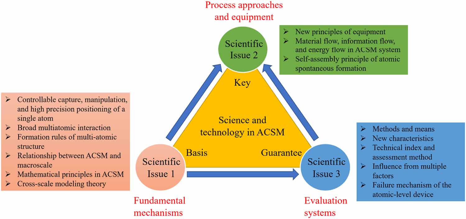
ACSM includes all of the steps necessary to transform the original materials or components into products that meet the users' needs, which involves not only atomic precision but also the manufacturing processes of removal, migration, and addition at the atomic scale. Comprehensive ACSM studies should systematically address the three types of common scientific issues in manufacturing at the atomic and close-to-atomic scales related to its fundamental mechanisms, process approaches, and evaluation systems, as shown in figure 2.

Figure 2. Main scientific and technological issues.
Download figure:
Standard image High-resolution imageScientific Issue 1: Principles of manipulating a single atom, the interaction mechanism of multiple atoms, and the relationship between ACSM and contemporary manufacturing.
The key to further development of ACSM lies in understanding the intrinsic mechanism of ACSM. When the object to be manufactured is at the atomic scale, traditional macroscopic processing theories cannot accurately describe and predict the mechanism of atomic removal, migration, or addition. More innovative studies on mechanisms are in great demand. Following the idea from fundamental research to application development, scientific issues in the intrinsic mechanism can be divided into monoatomic manipulation, multiatomic interaction, and multiscale coupling theory. As the new generation of manufacturing technology, ACSM will push manufacturing precision towards the atomic scale. The structure precision and reliability of each basic unit in ACSM are determined by the capture, controllable manipulation, and high precision positioning of a single atom, which directly affects the final performance.
Therefore, one aspect in ACSM mechanism research is to understand and learn the basic rules of manipulating a single atom, including the overall process of capturing, moving, and positioning of an atom. It means that the single atom needs to be captured stably, then migrated and positioned with high precision, and finally placed at a specified position of an atomic-level device. In this way, the fabrication accuracy of ACSM can be guaranteed to the atomic scale. Particle manipulation and its related technologies are less involved in other disciplines, hence new theories and methods are of significant need.
In ACSM, atomic-level operation is needed to build single-atom or multiatom structures, realizing the ultimate function of atomic-level devices. Therefore, the second aspect in the mechanism study of ACSM lies in understanding the broad multiatomic interaction, the formation rules of multiatomic structures, and the mechanism and degree of the influence on the performance of atomic devices. This issue is key for ACSM, from fundamental theories to applied technologies. In real physical space, both single and multiatomic structures interact with other atoms, i.e. there are one or more kinds of interactions existing in a wide range. At the macroscopic scale, objects are always subjected to gravitational forces, which can be described by Newtonian mechanics. However, the universal effects are not clear at the atomic and close-to-atomic scales. Equipped with the latest achievements in quantum theory, ACSM is expected to provide possible answers and experimental verifications for such effects. Further exploration of this issue will reveal the formation law of multiatomic structures and improve the final performance of atomic devices.
The third aspect of the mechanism study is to understand the relationship between atomic scale and the macroscale, including predicting the performance of ACSM functional devices in the macroscale. This is an important scientific issue to expand the application scope and ensure the performance of ACSM products. The macroscopic action of the device can be interpreted as the unified average performance of a large number of atoms acting simultaneously. For example, by calculating the motion of a large number of molecules, macroscopic parameters, such as the cutting force of material removal, can be predicted in molecular dynamics. There is a high degree of internal unification between the ACSM process and device performance because atoms are the common fundamental unit of both macroscale interaction and ACSM. Based on the mathematical description of atoms, the key to cross-scale research is to establish the ACSM mathematical system, e.g. creating multiscale physical and mathematical models, which is an important step in quantifying ACSM.
Scientific Issue 2: Energy directly acts on atomic basic manufacturing units
To realize ACSM, the scientific issues in the processing technique and equipment have to be solved. The ACSM manufacturing methods can be summarized as atomic removal, addition, and migration, together with other new means of manufacturing. Compared with the scientific issues in the mechanism study, this issue is the basis for the development of a large-scale, high-efficiency ACSM process. Current atomic-level processing approaches are either inefficient or have poor positioning accuracy. For example, the scanning tunneling microscope (STM) technique can manipulate one or several atoms at a time; but it is inefficient in mass production directly at the atomic scale. ALD and ALE can deposit or remove materials with atomic-layer resolution, but they are challenging when selectively depositing or removing the atoms at the position of interest. The critical scientific issue of improving efficiency and accuracy is how to apply required energy directly to a single atom or basic units of multiple atoms. For instance, the development principles of ACSM equipment need to be studied to form a manufacturing system; and the manufacturing activities need to be conducted at the scale of atomic devices. The core of this aspect is to understand and learn the movement of material flow, information flow, and energy flow in an ACSM system and to explore how to establish a universal multidimensional manufacturing system. Interatomic forces in ACSM cannot be ignored. It is important to understand and utilize the interatomic forces to study the self-assembly principle of atomic spontaneous formation of functional devices and develop both general and customized ACSM methods and equipment.
Scientific Issue 3: New characteristics of evaluation and measurements at the atomic and close-to-atomic scales
An ACSM measurement and evaluation system is another important issue to ensure the performance and reliability of ACSM products. At the atomic and close-to-atomic scales, structures in the atomic devices are maintained only by interatomic forces, which means the influence of measurement on the device should be as small as possible. The important scientific issues in the measurement include understanding the mechanism of influence and establishing the low-influence measurement theory that meets the requirements of ACSM.
Based on improving the measurement theory, the establishment of the evaluation system will make ACSM more standard, reliable, and efficient. The evaluation system of current manufacturing is established on the basis of macro-unified indicators of collective atoms. However, the basic units having a single atom or multiatoms in ACSM have a significant impact on the final performance of the devices; and the failure mechanism of the atomic-level devices is greatly different from that of the macrodevices. Therefore, the ACSM evaluation system needs a new theory and method to support. It is a significant scientific issue to establish an evaluation system to determine the effect of different processes and manufacturing parameters on performance. The critical scientific exploration in the evaluation system will be relevant to the influence principles on the final performance of atomic devices from different ACSM processing methods and parameters.
2.3. Main objectives and content
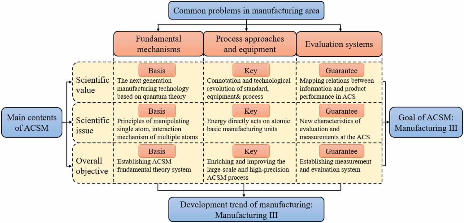
The overall target is to implement a complete and systematic ACSM process. This manufacturing process can be employed to take the necessary steps for converting original materials or components into atomic-level, functional components or products that meet users' requirements and ensure atomic-level precision and performance throughout the process. This requires tremendous innovation and breakthroughs in all aspects, including fundamentals, process methods, equipment, testing, and evaluation system. The establishment of the basic theory system based on atomic theory is the primary goal and necessary condition for the development of ACSM. Because the manufacturing activity is at the atomic and close-to-atomic scales, which is different from the current manufacturing theory, innovative study of ACSM fundamental theory is required. Enriching and improving the large-scale, highly efficient, and highly precise process is the main target of ACSM development. The new ACSM process needs the energy to directly act on atoms to establish a multidimensional manufacturing system with certain versatility. Under the action of interatomic forces, the atoms can spontaneously form specific functional structures to achieve large-scale, highly efficient, and highly precise manufacturing. The establishment of measurement and evaluation systems is an important means of determining whether it meets the requirements. The high-precision measurement method is the premise for ensuring the performance and reliability of ACSM products. The establishment of the evaluation system can make ACSM more standard, reliable, and efficient. The ultimate goal of ACSM is to lead the manufacturing sector entirely into Manufacturing III. This requires establishment of a new paradigm in the manufacturing field created from the common problems encountered in the studies of fundamental mechanisms, process methods, equipment, measurement and evaluation systems, and the related classical concepts. Figure 3 is a framework of the main content in ACSM that integrates scientific and technological values, issues, and main goals.

Figure 3. Main content of ACSM.
Download figure:
Standard image High-resolution image3. Significant needs
As the future manufacturing technology, ACSM breaks the clear boundary of the three modes of material addition, subtraction, and migration in the existing manufacturing process. It all boils down to single-atom action in extreme circumstances. The manufacturing object, process, and precision are all at the atomic scale, so the discretization of materials will make the quantum effect have a direct impact on the manufacturing process and the products. High-precision control and manipulation of an atom make it possible to process typical devices or components with extremely tiny scale and raise their performance to a new level. Such devices or components are difficult to produce by current manufacturing techniques, including chips in the post-Moore's law era (PME), cold atom gyroscopes, energy, new materials, and so on. ACSM involves multiple disciplines, such as machinery, physics, chemistry, life sciences, and materials. Devices and products manufactured are expected to be applied to various fields, such as the communications, information storage and computing, aerospace, energy, and medical sectors. In this article, PME chips and cold atom gyroscopes are taken as examples to see the emerging demands in wide industrial applications.
3.1. PME chips
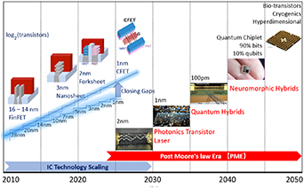
The semiconductor industry has been extremely effective in developing tools and processes that work well for making digital electronics, since the benefits from atomic-scale manufacturing dramatically improve manufacturing precision and reduce the size of the structural features. Currently, the absolute precision of chip manufacturing is extremely impressive, 7 nm or even less [34], but the relative precision is about ±10%. This poor relative precision is acceptable for digital electronics but fails for many other applications in nanoscale, which presents a major problem in technology advances in general. Thus, manufacturing precision must be further improved in the quantized nature of atomic and close-to-atomic scales. Figure 4 shows the roadmap to 1 nm by changing the transistor structure and the materials used one after another and optimizing the process. The 'IC technology scaling' part of figure 4 was developed by referring to Sarkar et al [35]. However, with the progress of miniaturization and integration, the manufacturing cost is rapidly increasing (it has doubled) due to the complexity of the process, in which the cost of the lithography step has increased by three times. For this reason, the manufacturing cost per transistor cannot be lowered as expected, and Moore's law is stalled.
Figure 4. Technology roadmap in developing PME chips.
Download figure:
Standard image High-resolution image
Emerging applications drive the incentive to develop atomically precise devices and technologies; and the most compelling is the next generation of chips, i.e. PME chips. On one hand, acceptable feature size variability of the classic integrated circuit chips is expected to be on the order of 3–4 atoms of silicon, including contributions from surface imperfections, in the next 5–10 years. On the other hand, quantum [36], phonics, and DNA computing will inevitably replace binary digital electronic computing, with the demand for processing huge sets of data in the future. Atomic precision features are critically required on those types of PME chips. The feature size of transducers and capacitors will become close to the size of an atom. PME chips based on hybrid models will also require atomic precision features. PME chips have greater information processing capabilities and the unique features of superposition and entanglement, which greatly improve the computing speed and storage capability. Taking quantum chips for instance, the technical difficulties in fabrication can be single quantum dots and highly complex quantum logic gates. Quantum dots, in a diameter of 2 nm (∼ 10 atoms per cluster), are allocated on atomically flat terraces separated by steps of only 0.22 nm in height [37]. The current processing of quantum logic gates mainly depends on femtosecond laser direct writing technology, which can deposit energy in a transparent medium; but it is difficult to accurately control the splitting ratio and waveguide phase [38]. Though a number of potentially complex and useful atomically precise products have been simulated, designed, or even prototyped, there are difficulties to commercially producing them for the market because of the lack of manufacturing precision at the atomic scale.
3.2. Cold atom interferometer gyroscope
The inertial navigation system has irreplaceable advantages in the high-tech field because of its self-determination, noninterference, large informative output, and strong real-time performance. The accuracy of the gyroscope directly affects the accuracy of the positioning and altitude output of the inertial navigation system. The cold atomic interference gyro, which is realized by using the Sagnac effect of the atomic de Broglie wave, is representative of the third-generation quantum matter wave gyroscope. With its ultrahigh measurement accuracy, it is becoming a hot research area in the field of inertial measurement [39, 40].
The cold atom interferometer uses atoms as sensitive media. Atoms are cooled, trapped, and manipulated by a laser, which interferes with the atomic wave packet due to the atom's energy level and wave property. In this way, an interference phenomenon similar to ring laser gyro is formed, the final interference fringes are measured, and the rotation and acceleration information of the carrier can be obtained. Atoms have the advantages of short de Broglie wavelength, long free evolution time, and narrow response frequency; and the interferometric phenomena are more abundant than photons because of the atom's mass, internal structure, and energy level. Therefore, the measurement accuracy is significantly improved. In the field of inertial navigation, atomic gyros are theoretically at least 1000 times more sensitive than optical gyros. The drift of a conventional inertial navigation system is about 1.8 km h−1, whereas the theoretical drift of an inertial navigation system based on a cold atomic interferometer gyroscope does not exceed 10 m h−1 [41, 42].
In the implementation of an atomic interferometer gyroscope, atom cooling, trapping, and manipulation requires the support of many optical devices. In order to ensure the precision and performance of the gyroscope, the traditional optical devices need to be redesigned, manufactured, assembled, and packaged rigorously, which makes the device large in size, highly complex, and great in cost. To capture atoms by portable devices without sacrificing precision, photonic integrated circuits can be used instead of conventional optical systems. Compared with a conventional discrete optoelectronic processing manner, a photonic integrated chip (PIC) can reduce costs and complexity. By integrating various optical components into one single chip, a large-scale, single-chip PIC greatly improves a system's size, power efficiency, and reliability and reduces the system cost. In addition, the application of photonic integrated chips can greatly reduce the number of independent optical components required by the transmission system and can also greatly reduce the optical component packaging. Atomic interferometer gyroscopes using photonic integrated circuits can significantly reduce the system size and outperform the original free space technology by one order of magnitude in terms of angular sensitivity and dynamic range [43]. ACSM is expected to break through the bottleneck of photonic integrated circuit fabrication and realize the stable manufacturing of a new type of atomic interferometric gyroscope.
4. Summary
ACSM is a new development phase in the field of manufacturing. Its fundamental concept is to directly apply energy to atoms, obtain specific functions and performance by constructing atomic-level structures, implement batch production, and meet the users' requirements.
ACSM has a theoretical framework that is completely different from that in the existing manufacturing. The underlying layer of the framework is no longer based on principles such as stress/strain, chemical equations, or traditional optics but is determined by quantum theory. The key to the further development of ACSM lies in understanding the intrinsic mechanism of ACSM. Fundamental science provides the theoretical basis for manufacturing, and the development of manufacturing promotes the fundamental research fields. The relevant theoretical research achievements are condensed in practice, which in turn is directly fed back to these research fields.
With the IC chip density approaching its limit and many other needs for functional feature size at the atomic scale, ACSM theories and technologies need to be planned in advance and deployed. ACSM will give a new impetus to the theory and technology of manufacturing, and it will also significantly promote the development of various fields. ACSM in its true sense of meeting the functional requirements of users will be realized, and manufacturing equipment with atomic precision will be developed.
When the study is at the atomic or close-to-atomic scale, the traditional macroscopic processing theory cannot accurately describe and predict the mechanism of atom removal, migration, or addition in the processed materials. Therefore, it is necessary to conduct deep and innovative research and development. Interdisciplinary research will be the source of great scientific achievements. To understand and apply the interatomic or polyatomic processes to the actual manufacturing process, the research on ACSM requires continuous academic exchanges among many disciplines, such as mechanics, physics, chemistry, materials, and life sciences. Through the contention of different academic viewpoints and the collision, exchange, penetration, and fusion of academic ideas, the technology of ACSMs can be rapidly established and well developed in the next 10 to 20 years.
As ACSM is a huge field in the next generation of manufacturing advancement and involves multidisciplinary areas, the view may be one-sided because of the author's limited knowledge. Through further investigation and discussion, this article hopes to initiate advancement of academia and industry in manufacturing.
Acknowledgments
The author would like to thank discussions with D Guo, J Yao, A Weckenmann, H. Kunzmann, K Ehmann, X Luo, J Zhang, N Yu, C Kang, H Duan, D Brabazon, G Yan and H Cui. Acknowledgement also goes to the consent for using the copyrighted content published in the journal of China Mechanical Engineering.
*Author Biography
Fengzhou Fang (FISNM, FAET, FCIRP, and FSME) is a joint professor and the director of Centre of Micro/Nano Manufacturing Technology (MNMT) at Tianjin University and University College Dublin. His research interests include fundamental studies and application development in the areas of optical freeform design and manufacturing, visual optics and bio-implants manufacturing, ACSM, and ultra-precision machining and measurement. He is also the Editor-in-Chief of Nanomanufacturing and Metrology.