
Abstract
Hard coatings are extensively required in industry for protecting mechanical/structural parts that withstand extremely high temperature, stress, chemical corrosion, and other hostile environments. Electrical discharge coating (EDC) is an emerging surface modification technology to produce such hard coatings by using electrical discharges to coat a layer of material on workpiece surface to modify and enhance the surface characteristics or create new surface functions. This paper presents a comprehensive overview of EDC technologies for various materials, and summarises the types and key parameters of EDC processes as well as the characteristics of resulting coatings. It provides a systematic summary of the fundamentals and key features of the EDC processes, as well as its applications and future trends.
Export citation and abstract BibTeX RIS

Original content from this work may be used under the terms of the Creative Commons Attribution 3.0 licence. Any further distribution of this work must maintain attribution to the author(s) and the title of the work, journal citation and DOI.
1. Introduction
Surface modification via hard coating is a process aimed at improving and modifying the surface of materials or workpieces in terms of mechanical, physical and biochemical properties [1, 2]. This process is essential for a wide range of advanced manufacturing technologies and the hard coatings have been applied to withstand extremely high temperature, pressure and hostile environments. A growing body of research has demonstrated the importance of surface modification in increasing the strength, corrosion resistance and wear resistance of material surfaces [3, 4] as well as generating new surface functions such as biocompatibility.
Enhancing material properties is crucial to the development of industrial products and the design and manufacturing of mechanical/structural components for extreme environments. In this area, surface modification via coating method plays a very important role in modifying the structural components of surface materials to enhance their resistance to abrasive wear, electrochemical corrosion and erosion [3–5]. Surface modification has also been used in various applications with the main purpose of enhancing the physical and biochemical properties of workpieces [1, 2].
In the biomedical field, specifically in dental and orthopaedic applications, surface modification has been applied on receiving body tissues to enhance the biomechanical and morphological compatibilities between the present and new receiving body tissues and to promote osteointegration [1]. Meanwhile, surface modification via plasma treatment can increase the adhesion and surface wettability, reduce tissue surface friction and remove contaminants to an acceptable level [6, 7]. Previous studies have offered consistent evidence on the importance of surface modification in the biomedical field, especially in modifying the outermost tissues surface and producing/fabricating the homogenous implant surface [7, 8].
Typical surface modification methods include carburising, electroplating and plasma spraying, which have been widely used in current industry [9]. Previous methods used for surface modification, including surface modification with material addition (coating) and without material addition (surface geometry, microstructure or chemistry modification), are listed in table 1.
Table 1. Surface modification methods with/without material addition.
| With material addition | Without material addition |
|---|---|
|
|
|
|
|
|
|
|
|
|
|
Recent developments in the field of surface modification have led to a renewed interest in electrical discharge coating (EDC), which modifies material surfaces by using electrical discharge energy [19]. EDC is a new technology which is derived from electrical discharge machining (EDM) by converting its electrode polarity [20]. Extensive research has been conducted to understand the fundamentals of EDC [4, 19, 21–27]. Figure 1 summaries the chronology of the development of the EDM/EDC technology [15, 28–43].
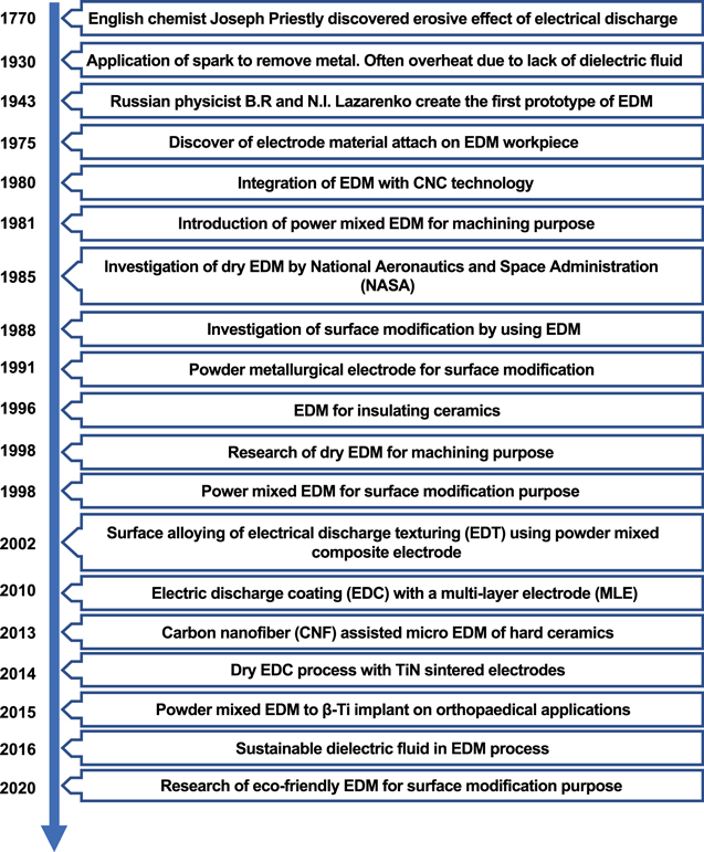
Figure 1. Chronology of EDM/EDC development.
Download figure:
Standard image High-resolution imageIn EDC, an extremely high temperature (8000 °C–12 000 °C) [44] is used to melt the electrode material and deposit it on the surface of workpiece. EDC is also able to modify the surfaces of all kind of electrical conductive materials, especially the extremely hard-to-machine materials, such as tungsten carbide [45] and silicon carbide [46].
However, to date, there is no available literature on a systematic review of the fundamental and applications of this highly promising technology. Especially, there is no systematic overview of the effects of EDC process parameters on the deposition characteristics of materials, including their deposited layer, corrosion resistance and wear resistance. To fill this gap, this paper presents a comprehensive review of various EDC methods for surface modification of various materials, particularly the process mechanisms and the roles of process parameters were compared in detail. It is expected that this paper provides practical guidelines for the development and application of EDC technology in the area of surface modification for high functionality products.
2. Fundamentals of EDC
Before introducing EDC, the fundamental of EDM is given for comparison. EDM, also known as EDM or spark erosion machining, is a common technology that uses electrode spark or discharge for eroding materials [47–50]. The arc was presented between the electrode and workpiece material. The gap distance between the material and electrode is very small, and a small crater forms after the spark or discharge [9]. The working principles of EDM are summarised as follows [51, 52]:
- EDM remove materials via the electrical discharge sparking between the electrode and workpiece;
- The electrode is connected to the cathode (negative terminal), whilst the workpiece is connected to the anode (positive terminal);
- The potential difference is applied to both the electrode and workpiece;
- A plasma channel is created due to the high potential difference applied to the electrode and workpiece;
- Both the electrode and workpiece are immersed in dielectric fluid, such as kerosene oil;
- The plasma channel collapses when the potential difference decreases;
- Such collapse sends a compressive shockwave to the electrode and workpiece;
- The surfaces of the electrode and workpiece melt as a consequence;
- A crater is formed as the molten material is flushed away by the dielectric fluid; and
- The whole process is repeated within a few microseconds.
EDC, also known as electrical discharge alloying (EDA), is an extension of EDM [53, 54] that uses a die-sinker EDM to deposit a layer of coating on the workpiece surface [55–57]. According to Moro et al [58], the EDC process follows the sparking principle, an alteration of the EDM process, to coat a certain amount of material on an uneven surface or complex shape. EDC modifies the surface of the workpiece to improve its performance, including its hardness and resistance to wear and corrosion [59, 60]. Therefore, the selection of a suitable electrode, powder suspension and other machining parameters, such as polarity, current, pulse duration and fluid concentration, have very important roles in ensuring a smooth process [45, 61, 62]. The working principles of EDC are summarised as follows [58, 63]:
- EDC almost has the same work mechanism as EDM. However, during the EDC process, the electrode is normally connected to the anode (positive terminal) and the workpiece is connected to the cathode (negative terminal);
- During the generation of electrical discharge sparks, the heat energy generated by sparks causes the breakdown of dielectric fluid and turns it into plasma form;
- As more energy provided, a plasma channel is formed and a spark strikes through the closest points between the electrode and workpiece;
- The energy generated by the spark triggers extreme heat which melts and vaporises the workpiece material in the plasma channel.
- After the spark, the plasma channel collapses, and the melted material from the electrode or dielectric fluid is deposited on the workpiece surface; and
- During each electrical discharge spark, the deposited material on the workpiece surface is solidified through a rapid cooling process (quenching) via the lower temperature of the dielectric fluid.
Based on the above-mentioned EDC working principles, EDC can create high-performance coatings which are useful for surface modification. As Wang [64] discussed, functionalization of a surface can be realised by modifying the surface property. EDC has very high potential to serve as an inexpensive surface modification method and fulfil the surface functionalization using conventional EDM machines [20]. However, EDC is still in its research phase and has not yet attracted wide usage in the industry [41, 65]. This is due to the lack of fundamental knowledge on the interactions between EDC working principles and the material properties [65]. Moreover, the lifetime and cost effectiveness of EDC is difficult to predict. For example, the reuse of powder mixed dielectric in powder-mixed electrical discharge machining (PMEDM) process is challenging [41].
While EDM is a material subtractive process, EDC is a material additive process by depositing materials on the surface of workpiece within a short period with a high current electrical pulse and presence of dielectric fluid [55, 66, 67]. Table 2 shows the differences between the EDM and EDC processes in terms of their function, polarity and machined surfaces. The schematic diagrams of EDM and EDC are presented in figures 2 and 3, respectively.
Table 2. Differences between EDM and EDC [21, 68, 69].
| Electrical discharge machining (EDM) | Electrical discharge coating (EDC) | |
|---|---|---|
| Definition | A material removal process that removes material from a workpiece to obtain the desired shape | A coating process that deposits a layer of material on a workpiece to achieve surface modification |
| Electrode polarity | The electrode or tool can be placed in either positive or negative terminal depending on the parametric condition (tool wear rate and material removal rate) | The electrode or tool is placed in anode (positive terminal) and the workpiece can be placed at cathode (negative terminal) |
| Weight of workpiece after processing | Decrease due to the material has been removed | Increase due to the deposited material (decrease in some case due to crater formation) |
| Function | To remove material on the surface of workpiece | To enhance the surface properties of workpiece |

Figure 2. Schematic diagram of EDM. Reproduced from [70]. With permission of Springer.
Download figure:
Standard image High-resolution image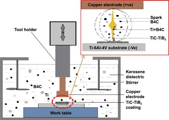
Figure 3. Schematic diagram of EDC. Reprinted from [71], Copyright 2017, with permission from Elsevier.
Download figure:
Standard image High-resolution image2.1. Modelling and simulation of EDC process
As it is difficult to directly observe the EDC phenomenon in EDC processes, modelling and computer simulation have been used for the prediction of EDC process parameters under certain conditions [72, 73]. In a previous research, Algodi et al [74] generated a model of EDC process which provided the estimation of the amount of energy transferred to the workpiece, along with predictions for crater geometry and microstructure development in EDC during cooling down. The modelling was done by using MATLAB software and verified by an experiment which could help to describe the fundamentals of the EDC processing to the cermet layers. At the end of the study, a model was successfully developed by which the prediction of the energy transfer was performed. Furthermore, Algodi et al [75] also carried out another modelling study where a 2D transient heat transfer model was developed by using finite difference methods in order to estimate the effective heat transfer into a workpiece during an EDC process. Apart from that, Das and Misra [4] conducted an experiment in order to compare the compatibility of artificial neural network (ANN) modelling and response surface methodology (RSM) modelling to the EDC process. They found that ANN modelling was more suitable than RSM modelling, although RSM modelling owned a lesser number of runs compared to ANN modelling.
2.2. Internal structure of EDC coating
Internal structure refers to the atom arrangement in the coating and in the interface between the coating and workpiece after the EDC process. During the EDC process, the coating material melted by heat and resolidified on the surface of workpiece, the solidified surface will then melt again by the spark, causing the change of compositional structure [67]. Due to the resolidification process, the structure that is closer to the surface will be in a form of amorphous while the structure that further from the surface will be in a crystalline form.
In the study of Murray et al [76], the structure of the EDC coating was observed by transmission electron microscopy (TEM). Figure 4 shows the cross sectional of TEM microstructure and the diffraction patterns in different locations. There were six points in an interval of 250 nm that were perpendicular from the coating surface have been chosen for observation. The structure closest to the coating surface (point 1) was a combination of amorphous structure and single crystal pattern, while at points 2 and 3, a combination of single crystal and a twinned pattern was observed. In locations 4, 5 and 6, solely single crystal pattern was observed.
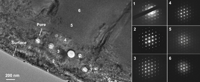
Figure 4. Bright field TEM image and the diffraction patterns in different locations. Reprinted from [76], Copyright 2013, with permission from Elsevier.
Download figure:
Standard image High-resolution imageMoreover, Algodi et al [22] investigated the grain size of the coated material by using TEM. Figure 5 presents the cross-sectional TEM micrograph of EDC coating layer. Region I owns a small grain size around 20–80 nm, and region II about 30–110 nm. Region III owns a columnar grain with the length of 330–450 nm and width of 90–140 nm, and region IV owns an intermediate grain size of 150–800 nm.

Download figure:
Standard image High-resolution image2.3. Comparison of EDC with other coating methods
In this section, a comparison of EDC process with other common type of coating methods (thermal spraying, physical and chemical vapour deposition and electroplating) will be given in terms of properties, mechanism, efficiency, and coating features [12, 13, 77]. Table 3 shows the comparison of EDC properties with others coating methods.
Table 3. Comparison of EDC with others coating methods.
| Coating methods | |||||
|---|---|---|---|---|---|
| Vapour deposition | |||||
| Electrical discharge coating (EDC) | Thermal spraying | Physical | Chemical | Electroplating | |
| Working environment/condition | Room temperature using conventional die-sinker EDM | Room temperature using a spray gun with a stream heated by oxyfuel flame, electric arc, or plasma arc | High vacuum and temperature (200 °C–500 °C) | High temperature (950 °C–1050 °C), atmospheric pressure and inert atmosphere | Room temperature with two electrode supply by electricity |
| Substrate/workpiece | Conductive metals | Any materials | Any materials | Any materials | Conductive metals |
| Coating material | Any materials | Metals, alloys, carbides, ceramics and polymers | Metals or ceramics | Metals or ceramics | Metal ions |
| Post coating process | Clean the dielectric fluid and let dry | Clean the oil and dirt then roughened (e.g.: grit blasting) to enhanced bond strength | Clean the surface | Clean toxicity exhaust gas with scrubbers and need 6–8 h for cool down to room temperature | Clean and let dry to prevent oxidation |
| Coating efficiency | High | High | Low | Low | Intermediate |
| Function of coating | Enhance the characteristics of the original substrate in term of hardness, roughness, corrosion and wear resistance | Resist wear and corrosion | Improve hardness, wear resistance and oxidation resistance | Able to produce uniform thickness of coating with low porosity, even on substrates with complicated shape | Resist wear, corrosion, high electrical conductivity and reflectivity |
| Application | Bio-compatible implantation, mould and die industry | Aircraft engine components, storage or car tank, rocket motor nozzles, crankshafts and valves | Aerospace, automotive, surgical/medical, dies and moulds | Cutting tool | Electronic industry (semi-conductor and printed circuit board) |
| Other features | Able to achieve high hardness and low roughness mirror-like surface | Good toughness, good surface fatigue resistance and low residual tensile stress | Excellent throwing power, able to produce thin, uniform and low porosity coatings. Great capability of localised, or selective deposition, on patterned substrates | High coating purity, great adhesion between coating and substrate, excellent coverage | |
2.4. Coating mechanisms and features
Up to now, little attention has been paid to compare the coating mechanisms of EDC with those other common coating processes. In this section, a critical comparison of coating mechanisms of EDC process with thermal spraying, vapour deposition and electroplating will be given. To assist the comparison, schematic diagrams of EDC, thermal spraying, vapour deposition and electroplating are shown in figure 6.

Figure 6. Schematic diagrams for (a) EDC [79], (b) thermal spraying [80], (c) vapour deposition [81] and (d) electroplating [82].
Download figure:
Standard image High-resolution imageThe EDC process is mainly carried out by using conventional EDM machines. An electrical discharge or sparking will occur when both electrode and workpiece immerse into the dielectric fluid. A plasma channel or ionisation channel is created between the gap of electrode and workpiece. The generation of extremely high temperature in the range of 8000 °C–12 000 °C causes erosion and vaporisation of both the electrode and workpiece [44, 78]. Under suitable process condition and parameters setup, material transfer occurs from the working fluid or suspended powder or electrode to the surface of workpiece. The material transfer may occur in a free form (elements form) or carbides form by combining with the carbon elements due to the long carbon chain of hydrocarbon dielectric fluid. This process generates new compositions of workpiece surface and subsequently processed by quenching and hardening process [78].
Thermal spraying is a process developed by modifying oxy-acetylene torches. The coating materials are available in the form of wire, rod, granular and powders. The materials are fed through central passage by gas stream or from canister which mounted directly on top of the gun. The materials are then transport into the burning flame and the stream gases continue bring the materials toward the prepared substrate surface. However, this process will cause a high oxide inclusion in metals due to extreme heat of material react with oxygen in the air. Generally, metals and alloys are use as the coating materials while where the flame temperature in the normally will reach from 2800 °C to 3200 °C [83].
Physical vapour deposition (PVD) is a coating method that deposits material on the substrate by the transfer of material at the atomic level. The process will first convert the material from a solid state to a vapour state. Then the vapour will transport to a region of lower pressure where also near to its substrate. After that, the vapour will undergo condensation and deposited on the substrate as a thin film with only the thickness of an atom [84]. However, chemical vapour deposition is commonly used to deposit the metallic or ceramic compound on the surface of workpiece. The process works by depositing the material through the condensation from a gaseous phase to solid phase. This process can be achieved by the chemical reaction between volatile form of coating material and the surface of the substrate. As the volatile coating material will pass over the heated substrate surface and the chemical reaction will turn the volatile coating material to solid form, which result it deposited onto the substrate [11].
In electroplating, electrons are supplied to ionic metal to form a coating on a substrate. Electroplating uses electricity to reduce the charge of cations (ionic metals) from electrolyte and deposit a conductive thin layer on the cathode (substrate). Electroplating usually involves an electrolyte solution with the ionic form of desire coating material, a cathode (negatively charged) where electrons will be supply to turn the ionic metal to non-ionic metal by reducing the charge, and an anode (positively charged) made by electrical conductive material which usually will differentiate to soluble anode (made by the coated material, which will eroded and deposit on cathode) and insoluble anode (made by carbon, platinum, titanium, lead or steel, which will not eroded and the coated material will supply by ionic metal in the electrolyte solution) [14].
To sum up, there are a lot of coating methods for surface modification. All of these methods are able to enhance the surface properties and reduce production cost by using a few materials to replace those expensive and non-renewable material [85]. However, except the EDC process, all of these coating methods need a special apparatus setup and machining condition such as special vacuum apparatus and elaborate pre-cleaning process. Besides, for the coating layer thickness and coating area of thermal spraying, vapour deposition and electroplating cannot be controlled well, unlike EDC process. Therefore, EDC process is a unique method for surface modification especially for industrial purposes, such as mold and die repairing and performance enhancing in terms of hardness, corrosion and wear resistance. Table 4 shows a summary of coating features between EDC, thermal spraying, vapour deposition and electroplating [3, 21, 26, 86–104].
Table 4. Summary of coating features between EDC, thermal spraying, vapour deposition and electroplating.
| Coating methods | |||||
|---|---|---|---|---|---|
| Vapour deposition | |||||
| Electrical discharge coating (EDC) | Thermal spraying | Physical | Chemical | Electroplating | |
| Hardness (HV) | 149.03–1929 | 1231–1298 | 540.4–3477 | 1685–2012 | 300–1070 |
| Layer thickness (μm) | 3–112 | 75–475 | 0.001–3 | 0.001 429–0.266 | 1–685 |
| Corrosion potential (V) | −0.402–2 | −0.619 to −0.710 | −0.44 to −0.13 | −0.617 to −0.496 | 0.5–1.2 |
| Wear resistance (Coefficient of friction) | 0.2–0.55 | 0.20–0.31 | 0.324–0.635 | 0.2–0.8 | 0.18–0.25 |
3. Surface modification methods by EDC
3.1. EDC with powder metallurgical electrodes (PM electrodes)
Many studies [19, 105, 106] have defined EDC as a process that modifies the surface by depositing materials on the substrates. One of the methods for performing EDC is by using die sinking EDM with PM electrodes. In this process, the material of the electrode is transferred from the positive terminal to the negative terminal (workpiece) when sparking. At this moment, a plasma channel is created between the electrode and workpiece to generate heat energy [65, 107]. This energy then melts and vaporises certain areas of the workpiece and PM electrodes. The melted materials are then solidified by the dielectric fluid and are deposited on the surface of the workpiece.
In their analysis of coating characteristics, Das and Misra [21] claimed that EDC with TiC–Cu green compact electrode can increase the micro-hardness of aluminium base material from 155 HV to 1800 HV. A 51.24 μm thick coating layer was successfully achieved after the EDC process. They also highly recommended the EDC process in various industrial applications given its low cost and no need for any additional or special equipment. Gill and Kumar [108] also found that the coating produced by the Cu–Mn PM electrode has higher concentrations of manganese (Mn, 5.05%) and carbon (C, 6.12%) compared with the H11 hot die steel base material (0.346% and 0.349%, respectively), which contributed to increasing the micro-hardness of the material from 615 HV to 1191.7 HV (about 93.7%). They also found some copper (Cu) elements on the coating surface, which can help to enhance the corrosion resistance of the material. They suggested the application of this technology in the manufacturing of H11 die mould.
Figure 7 illustrates the EDC process with PM electrodes. The types of dielectric fluids, workpieces, PM electrodes, compaction loads and compositions used in previous research are summarised in table 5.
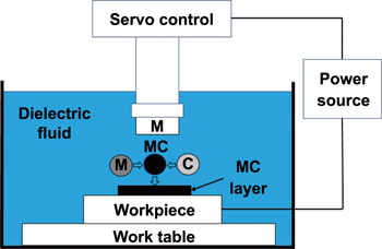
Figure 7. EDC by powder metallurgy method. Reproduced with permission from [27].
Download figure:
Standard image High-resolution imageTable 5. Summary of the EDC by powder metallurgy method.
| Type of workpiece | Type of dielectric fluid | Type of electrode | Composition (%) | Compaction load (ton) | References |
|---|---|---|---|---|---|
| Aluminium | Kerosene | TiC–Cu | 50–50, 60–40 and 70–30 | 2, 3 and 4 | [21] |
| 304 stainless steel | Shell Paraol 250 | Ti–C | — | — | [22] |
| Aluminium | Hydrocarbon oil | Ti–B4C | 81–19 and 72–28 | 1.77 and 2.36 | [24] |
| Aluminium | Hydrocarbon oil | W–Cu | 50–50 | 1.5 and 2 | [27] |
| AISI 1020 mild steel | Hydrocarbon oil | TiC–Cu | 60–40, 70–30 and 20–80 | 3 | [27] |
| ZE41A magnesium alloy | EDM oil | WC–Cu | 50–50 | 1.2, 1.4 and 1.6 | [54] |
| Inconel 718 alloy steel | EDM oil | Cu–W | 20–80 | — | [69] |
| Aluminium | Hydrocarbon oil | Ti–Al | 64–36 | 2.01–11.04 | [109] |
| AISI 1020 mild steel | EDM oil | TiC–Cu | 60–40 and 70–30 | 5.3 | [110] |
| Mild steel | EDM oil | WS2-Cu | 40–60, 50–50 and 60–40 | 0.35 | [111] |
| Aluminium | Kerosene | SiC–Cu | 30–70 and 50–50 | 5, 10, 15 and 20 | [98, 112] |
| Aluminium | Hydrocarbon oil | W–Cu | 75–25 | 5, 10, 15 and 20 | [19, 113–115] |
3.2. EDC with multi-layer electrodes
A multi-layer electrode was fabricated by alternately stacking more than one material and fastening them with a jig [43]. Applying this electrode in the EDC process can improve the surface hardness of the workpiece, reduce the surface roughness of the coating layer, reduce the presence of microcracks on the surface of the coating layer and improve the stability of electricity discharge and machining time [10, 43].
During the EDC process with multi-layer electrodes, Hwang et al [43] reported that the coating produced by multi-layer titanium (Ti) and graphite electrodes has an average hardness of 1216.0 HV, which is higher than that of the nickel workpiece (250.0 HV). They also found that the coated layer demonstrates excellent abrasion resistance at room temperature (30 °C) and at higher temperatures (400 °C) due to its low coefficient of friction (CoF) as revealed in the abrasion resistance test. This finding is consistent with the conclusions of Murray et al [56], who found that the EDC process with a multi-layer electrode has a very strong melting point to resist the ejection resulting from the increasingly rapid solidification. The nanoindentation also shows that the coating has a higher mean hardness (11.0 GPa) compared with 304 stainless steel workpieces (1.90 GPa).
Figure 8 and table 6 illustrate the EDC process with multi-layer electrodes and summarises of the previous research using these electrodes, respectively.

Figure 8. EDC with multi-layer electrode. Reprinted from [43], Copyright 2010, with permission from Elsevier.
Download figure:
Standard image High-resolution imageTable 6. Summary of EDC using multi-layer electrode.
| Type of workpiece | Components of multi-layer electrode | Type of dielectric fluid | References |
|---|---|---|---|
| SKD 61 steel | Graphite and copper | Jatropha curcas fluid and kerosene | [10] |
| 304 stainless steel | TiC, Si, Cu, WC and Zr | Shell Paraol 250 | [56] |
| Nickel | Titanium and graphite | Castrol (SE Fluid 180) | [43] |
3.3. EDC with powder suspension or PMEDM
Figure 9 illustrates the use of PMEDM in the EDC process. According to Kansal et al [116], PMEDM is a technology that was introduced in 1980 to enhance the performance of machines. In PMEDM, a bridging phenomenon occurs at the plasma channel (spark gap) between the electrode and workpiece due to the interlocking amongst the powder particles along the current flow direction [107, 117]. A faster sparking occurs as the electrical discharge leads to the erosion of the workpiece and increases the material removal rate (MRR) [118]. At the same time, the powder suspension fills in the plasma channel and subsequently reduces the electric density and occurrence of abnormal discharge [119]. The surface of the workpiece is then modified as the electrical discharge is uniformly distributed and a shallow crater is formed on the workpiece surface.
Figure 9. EDC by powder suspension method. Reprinted from [116], Copyright 2007, with permission from Elsevier.
Download figure:
Standard image High-resolution imageMeanwhile, the addition of surfactant to the dielectric fluid will enhance the conductivity and dispersion of suspended powder in the dielectric fluid, increase the tension of the dielectric fluid and reduce the agglomeration of suspended powder at the bottom of the EDC tank [120–122]. The working principles of PMEDM are summarised as follows [116]:
- A powder material is prepared and mixed with dielectric fluid;
- The electrode or tool is normally connected to the anode (positive terminal), whilst the workpiece is connected to the cathode (negative terminal) to achieve a low- or no-wear electrode process;
- A plasma or ionisation channel is formed between the surfaces of the electrode and workpiece;
- The generation of electrical discharge sparks in the plasma channel melts the powder suspension in the dielectric fluid and deposits the material on the workpiece surface;
- This phenomenon can be ascribed to the melting and vaporisation process in the plasma channel at a very high temperature of electrical sparking;
- During each electrical discharge spark, the deposited powder material on the workpiece surface is solidified via a rapid cooling process (quenching); and
- The deposited powder material bonds with the surface of the workpiece to create a layer of coating.
Based on the previous research, the advantages of powder additives to the EDC process include reducing the surface roughness and tool wear rate (TWR), improving the topological properties of the workpiece (i.e. reduced micro-pores and micro-holes), enhancing the corrosion resistance of the workpiece, producing a no-burr and no-stress workpiece, creating a mirror-like surface, reducing the insulating strength of dielectric fluid, increasing the spark gap between the tool and surface of the workpiece, flushing uniform debris to ensure a stable EDC process and improving the electro discharge frequency [33, 62, 123, 124].
According to Janmanee and Muttamara [45], the coating produced by the EDC process with a Ti powder suspension can enhance the micro-hardness of the WC–Co base matrix from 990 HV to 1750 HV. This process can also effectively eliminate micro-cracks and voids to modify the surface of workpiece.
In the biomedical field, Prakash and Uddin [3] proved that the EDC process using hydroxyapatite (HA) powder in deionised water can produce a crack-free biomimetic non-porous HA-containing layer on the β-Ti implant substrate. The HA-containing coating layer has an 18 μm to 20 μm thickness, a very strong interface strength and a mechanical interlock with the β-Ti implant substrate. According to the results of the in vitro bioactivity analysis, the HA-containing coating can enhance the cell attachment and has a higher cell proliferation compared with the original surface. The previous studies on the powders used for EDC via PMEDM are summarised in table 7.
Table 7. Summary of powders used for EDC by PMEDM method.
| Type of workpiece | Type of electrode | Type of dielectric fluid | Type of powder used | Particle size of powder (μm) | Concentration of powder (g l−1) | References |
|---|---|---|---|---|---|---|
| β-Ti alloy | Cp-Ti | Deionized water | HA | 0.5–1 | 0, 5, 10 and 15 | [3] |
| Tungsten carbide | Cu | Shell EDM fluid 2 A | Ti | <36 | 50 | [45] |
| 65%SiC, 10%SiC-5% quartz/Al, 30%SiC | Cu, graphite, Cu- graphite | EDM oil | Cu and graphite | 5 | 6 | [46] |
| H11, HCHCr and AISI 1045 | Graphite, W–Cu and brass | Kerosene and EDM oil | Si, graphite and W | 36 | 0, 5 and 10 | [50] |
| AISI H13 tool steel | Cu | Hydrocarbon oil | Mo | <15 | 3 | [59] |
| Al 6061 | Cu | EDM LS kerosene | W | <50 | 8 | [61] |
| Titanium–tantalum alloys | Grade 2 pure Ti | Deionized water | HA | 0.5 | 0, 5, 10 and 15 | [118] |
| Grade 4 pure Ti disc | Grade 4 pure Ti | Deionized water | Ti | 35–45 | 3 and 6 | [125] |
| Plastic mold steel | Cu | Tap water | SiC | — | 5, 10 and 15 | [126] |
| AISI H13 tool steel | Cu | Hydrocarbon oil | Si and Mn | <5 and <10 | 5, 10 and 15 | [127] |
| β-Ti alloy | Cp-Ti | Hydrocarbon oil | Si | — | 4 and 8 | [128] |
| Ti–6Al–4V alloy | Cu | Kerosene | Ti–B4C | 8–10 (Ti) and 10 (B4C) | 10 | [71] |
| Ti–6Al–4V alloy | Cu–W | — | Al | 0.04 | 1–3 | [129] |
| AISI-D2 die steel | Cu | Kerosene | CNTs | — | 0.002, 0.004 and 0.006 | [130] |
| Carbon steel (AISI 1049) | Cu | EDF-K (Mitsubishi Oil) | Ti | <36 | 50 | [131] |
| Be Cu alloys | Cu | Commercial EDM oil | Al2O3 | 150 | 2, 4, 6 | [132] |
3.4. Dry EDC
Dry EDC is an additive EDC process that uses gas, such as argon and oxygen, as a dielectric medium to reduce the cost of liquid or oil-based dielectric fluid. Dry EDC can overcome environmental pollution problems by preventing the EDC process from producing any by product and helps avoid hazards to human health [120].
In 2006, Chen and Wu [29] found that the dry EDC process with high- or low-density TiN electrodes can create pure TiN layers on the aluminium surface. However, only the high-density TiN electrodes can be sustained under high discharge energy given that their wear rates are lower than those of low-density TiN electrodes. Moreover, based on the coating surface morphology, a dense fine granular surface can be found when a low peak current is applied, whereas a coating surface with a porous network appearance and high surface roughness is formed when a high peak current is applied. The working principles of dry EDC are summarised as follows [29, 100, 133, 134]:
- A steel chamber is prepared and installed on the bench of a conventional die-sinker EDM;
- A certain type of gas (usually O2, N2 or Ar2) is prepared as dielectric medium and connected to the steel chamber for the dry EDC process;
- A PM electrode is used and mounted at the anode (positive terminal), whilst the workpiece is mounted at the cathode (negative terminal) of the conventional die-sinker EDM;
- After adjusting the gap between the electrode and the surface of the workpiece, the steel chamber is sealed to trap gas during the dry EDC process;
- The gas is supplied with uniform pressure and the electrode is rotated at a constant rotational speed. The entire process is performed in a dry environment; and
- The material is then transferred from the electrode to the surface of the workpiece by the gas medium supply, and a layer of coating is then formed on the workpiece surface.
In their analysis of dry EDC with the Ti powder compact electrode, Chen et al [133] found that an excessive electrical discharge energy during the dry EDC process leads to the self-propagating high-temperature synthesis reaction of the Ti powder compact tool, which in turn may result in the low quality of the coating layer and instability of the dry EDC process. Therefore, Chen et al proposed the following parameters that can guarantee the stability of dry EDC under 5 kg cm−2 N2 pressure with 100 rpm electrode rotation: IP = 5 A, TON = 18 μs, duty factor = 15%; IP = 5 A, TON = 25 μs, duty factor = 11% and IP = 10 A, TON = 18 μs, duty factor = 6%.
Apart from that, Chen and Wu [100] performed a detailed dry EDC process by using a conventional die-sinker EDM with a closed chamber that is connected to a high-purity nitrogen gas cylinder. They opened the regulation valve for about 5 min to insert high-purity nitrogen gas into the chamber and to remove residual oxygen gas. The nitrogen gas was maintained at a pressure of 5 kg cm−2 and the electrode was set at 100 rpm rotational speed throughout the entire dry EDC process. Figure 10 illustrates the dry EDC process and table 8 summarises the dry EDC conditions used in previous research.
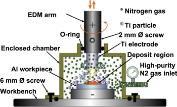
Figure 10. Dry EDC process. [100] Copyright © 2014, Springer Nature. With permission from Springer.
Download figure:
Standard image High-resolution imageTable 8. Summary of conditions used in dry EDC.
| Type of workpiece | Type of electrode | Electrode rotational speed (rpm) | Type of dielectric medium | Pressure of dielectric medium (kg cm−2) | References |
|---|---|---|---|---|---|
| Aluminium alloy (6061) | Sintered TiN ceramic | 100 | N2 | 5 | [133] |
| Ti50Ni50 shape memory alloy (SMA) | Ti pipe | 120 | N2 | 1 | [134] |
| Aluminium alloy (6061) | Pure Ti | 100 | N2 | 5 | [29, 100] |
4. EDC parameters
4.1. Peak current
The behaviour of peak current was first studied in 1983 by Jameson [135], who found that when turning on the power supply, the electricity flows from the power source to the machine. The initial current flows into the device and then increases until it reaches its highest value, also called as peak current (Ip). Peak current is generally defined as the maximum amount of current that provides support to the output to perform a certain task. In the case of EDC or EDA, the peak current is defined as the highest input current that generates the spark between the electrode and workpiece immersed in dielectric fluid [135]. Moreover, Bröcking et al [136] highlighted the relationship between Ip and the ionisation process and found that the current flow from the power supply to the electrode during the EDC process leads to the ionisation of dielectric fluid in the spark gap. When the ionisation temperature exceeds 7726.85 °C, the electrode and workpiece surface start to melt and vaporise.
Janmanee and Muttamara [45] used different peak currents (10, 15, 20 and 25 A) to deposit a layer of Ti on a tungsten carbide (WC) surface. They found that the optimum coating layer is approximately 20.32% percentage by weight at 20 A, thereby suggesting that a 20 A current allows the Ti powder to fill up the microcracks and craters on the surface of WC. However, the bonding capability decreases as the current exceeds 20 A. The relationship between the percentage by weight of Ti coating and the current is illustrated in figure 11.

Figure 11. The relationship between the Ti coating and current. Reprinted from [45] Copyright 2012, with permission from Elsevier.
Download figure:
Standard image High-resolution imageIn the same regard, a recent research by Tyagi et al [137] to produce MoS2 + Cu coating on a mild steel via PMEDM method proved that peak current was a significant factor to the coating layer thickness. A minimum coating layer thickness 0.446 mm was obtained when a low peak current 4 A was applied, and a maximum coating layer thickness 0.647 mm was achieved at a high peak current 10 A. This phenomenon occurred due to the high peak current triggered strong sparks and led to more material melted and finally deposited on the surface of mild steel.
On the other hand, Rahang and Patowari [115] found that electrode erosion is triggered by the energy generated by the peak current. A low current generally corresponds to a low TWR. Nevertheless, the erosion rate and Ra increase along with the current setting. Rahang and Patowari reported highest TWR and surface roughness of 49.02 mg min−1 and 9.5 μm Ra with a peak current setting of 6 A, respectively. Similarly, Das and Jain [138] found that the TWR of the TiC–Cu green compact electrode increases along with the peak current due to the formation of craters. They also reported that an increase in peak current generates a large amount of spark erosion and increases the tool material deposition on the workpiece surface. Therefore, an increasing peak current influences the increase in material deposited rate (MDR).
Apart from triggering an electrode erosion, an increasing peak current can also worsen the surface roughness of the workpiece during the process. This conclusion has been supported by Gill and Kumar [139], who found that increasing the peak current will also increase the surface roughness and micro-hardness. The discharge energy increases along with the peak current, thereby increasing the surface roughness. At higher peak currents, the sparking towards the workpiece grows in intensity. As a consequence, more molten materials are ejected out from the crater of the workpiece, which in turn increases the surface roughness. The micro-hardness also increases along with the current as a result of the frequent heating and quenching of the material throughout the process.
Prakash and Uddin [3] reported that a high HA powder concentration (15 g l−1) with a high peak current (15 A) and low pulse duration in deionised water deposits a uniform and crack-free HA layer on the surface of the β-phase Ti implant. However, this conclusion was opposed by Ekmekci et al [126], who found that the surface cracks are formed by the diffusion of C into the recast layer from the particle and that the penetration of C particles decreases along with the peak current. Therefore, the cracking of the coating surface reduces along with a lower peak current.
In sum, the PMEDM and PM electrode methods are the most commonly adopted approaches in the literature. Therefore, the following subsections shall only focus on these two methods. The peak current ranges employed in previous research are summarised in figures 12 and 13 and are classified based on the workpiece used.

Figure 12. Range of peak current used in EDC by PMEDM method.
Download figure:
Standard image High-resolution image
Figure 13. Range of peak current used in EDC by powder metallurgical electrode method.
Download figure:
Standard image High-resolution image4.2. Discharge voltage
According to Jameson [135], in the case of electricity, voltage refers to the electromotive force, electrical pressure and force. Meanwhile, in EDM, voltage refers to the pressure that allows the current to pass through in the form of a spark.
Ranjan [110] and Gill and Kumar [139] discovered that discharge voltage can be described based on the spark gap between the electrode and workpiece and the dielectric breakdown strength. Plasma is created when the open gap voltage rises to a level that allows the current to flow into the system. The voltage decreases again after the current flows into the system and stabilises the spark gap level. They also argued that the width of the spark gap between the surface of workpiece and the bottom edge of the tool electrode is influenced by discharge voltage. The width of the spark gap increases along with discharge voltage due to the improvements in the flushing condition and can help control the machine stability. As the discharge voltage increases, the values of surface roughness, TWR, MRR and micro-hardness also increase because a rise in voltage can trigger the growth of spark or discharge energy [110, 139].
Moreover, Prakash et al [140] found that voltage posed a significant factor to the recast layer thickness. They claimed that as voltage increased from 20 to 40 V, more heat energy was transferred to the Ti6Al4V electrode. This phenomenon triggered the melting of electrode and intensified penetration into the nickel workpiece and increased the recast layer thickness.
Liew et al [141] reported a large quantity of deposited W particles at a low voltage of 60 V. However, this quantity decreases when the voltage rises to 110 V because the spark gap between the workpiece and electrode becomes larger as the voltage increases. Therefore, the W particles become more easily flushed out from the surface of workpiece, thereby reducing the amount of deposited materials.
Figures 14 and 15 show the discharge voltage ranges adopted in previous research that use the PMEDM and PM electrode methods, respectively.
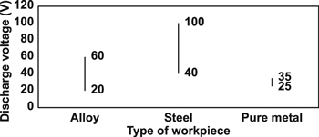
Figure 14. The range of discharge voltage used in EDC (PMEDM method).
Download figure:
Standard image High-resolution image
Figure 15. The range of discharge voltage used in EDC (powder metallurgical electrode method).
Download figure:
Standard image High-resolution image4.3. Pulse on time
Pulse on time can be defined as a spark on time [135], which is an important input parameter for the EDC or EDA process. When the current passes through from the power supply to the machine, a spark is generated between the electrode and workpiece. The electric discharged during the pulse on time. A longer pulse or spark on time corresponds to a larger amount of eroded electrodes [20].
Jameson [135] argued that both the spark on and spark off times are measured in microseconds (μs, or one-millionth of a second) and usually range from 1 to 250 μs. When both spark on and spark off times have the same length, a machine generates 2000–500 000 sparks per second.
Gill ad Kumar [139] analysed the effect of pulse on time on surface roughness and argued that the surface roughness improves along with a low pulse on time because a small spark area is generated when a low pulse on time is applied. As a result, a small crater is formed on the workpiece surface and an improved surface roughness value is obtained [139]. These results corroborate the ideas of Prakash et al [142] who discovered that discharge crater becomes wider and deeper as the pulse on time increases. This phenomenon is due to the discharge energy proliferates and penetrates into the surface of substrate and causes the material removed from the surface of workpiece with a wide and deep crater.
According to Rahang and Patowari [115], pulse on time can control the amount of tool wear by setting the time duration for each pulse of energy discharged. A lower pulse on time corresponds to lesser tool erosion induced by spark energy and a lower TWR. Similarly, the material transfer rate (MTR) depends on pulse on time. In the case of EDC using the PM electrode method, a higher pulse on time corresponds to a higher MTR due to the increase in TWR. This conclusion has been proven by the results of this work, which show that an MTR of 6.8 mg min−1 can be achieved at a pulse on time of 2000 μs. This result is also consistent with the conclusions of Das and Jain [138] and Tijo and Masanta [106], the latter of which revealed that both TWR and MDR increase along with pulse on time given the high temperature and erosion of the W–Cu powder metallurgy tool. However, Tijo and Masanta added that both TWR and MDR decrease when the pulse on time increases from 200 to 300 μs. This is due to the pulse diameter increase, energy density on the spark spot decrease at 300 μs and the energy loss does not contribute to the removal of materials from the W–Cu powder metallurgy tool. Therefore, both TWR and MDR decrease when the pulse on time increases from 200 μs to 300 μs.
The pulse on time ranges used in previous EDC research that apply the PMEDM and PM electrode methods are summarised in tables 9 and 10, respectively.
Table 9. The range of pulse on time used in EDC (PMEDM method).
| Workpiece | Range of pulse on time used by previous research (μs) (PMEDM method) |
|---|---|
| β-Ti alloy | 5–80 |
| AISI steel | 6.4–150 |
| Tool/Mold steel | 25–400 |
| Ti–6Al–4V alloy | 64–200 |
| Al alloy | 5–100 |
| Ti–Ta alloy | 50–150 |
| MMCs | 10–50 |
Table 10. The range of pulse on time used in EDC (powder metallurgical electrode method).
| Workpiece | Range of pulse on time used by previous research (μs) (PM electrode method) |
|---|---|
| Al alloy | 4–1010 |
| Die steel | 20–300 |
| Stainless steel | 2–64 |
| WC–Co | 50–250 |
| AISI steel | 20–135 |
4.4. Pulse off time
Mussada and Patowari [19] referred to pulse on and pulse off times as pulse duration and pulse interval, respectively. Specifically, during the pulse duration (pulse on time), the material is transferred from the PM electrode or powder suspension to the workpiece surface, whereas during the pulse interval (pulse off time), the electrical discharge or spark is minimised and the energy supply is inhibited. In addition, no material transfer occurs during the pulse interval, but the flushing of dielectric fluids will continue removing debris and the deposited material will undergo a rapid cooling process. After this rapid cooling process, the materials are deposited on the solidify layer again in the subsequent pulse duration. This cycle, which continues throughout the machining time, can result in a layer-by-layer deposition of materials on the workpiece surface [19]. These results are similar to those reported by Vijayakumar and his co-workers [68], who defined pulse off time as the moment where the pulse relaxes and a dielectric reionisation occurs. The temperature of the plasma channel between the gap of electrode and the workpiece reduce during the pulse off time. Moreover, pulse off time also can control the stability of servo control during the EDC process [68].
Nevertheless, Zain and his co-workers [143] argued that pulse off time does not significantly influence the micro-hardness of the coating. However, when the pulse off time increases from 5 to 9 μs, the micro-hardness of the coating on the stainless steel workpiece increases from 600 HV to 800 HV. They attributed such increase of micro-hardness to the stainless steel is due to the surface alloyed by the TaC powder added to the dielectric fluid. Besides, a recent study by Algodi et al [74] mentioned that when applying a semi-sintered TiC electrode on the surface of stainless steel workpiece, the temperature near the surface of the molten material rapidly reduces from 20 000 to 4000 K within 10 μs of pulse interval, followed by a low uniform cooling rate of about 100 μs. This rapid cooling phenomenon is triggered by the heat transfer between the molten material and the circulate dielectric fluid. This phenomenon may be also explain why the micro-hardness of the workpiece increases along with pulse off time.
The pulse off time ranges used in previous EDC research that employ the PMEDM and PM electrode methods are summarised in figures 16 and 17, respectively.
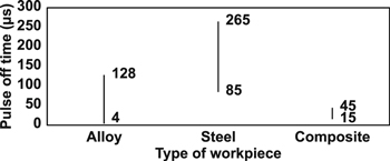
Figure 16. The range of pulse off time used in EDC (PMEDM method).
Download figure:
Standard image High-resolution image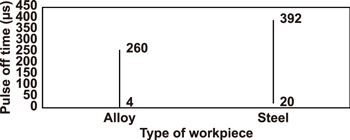
Figure 17. The range of pulse off time used in EDC (powder metallurgical electrode method).
Download figure:
Standard image High-resolution image4.5. Duty factor or duty cycle
According to Jameson [135], the whole system takes time to recharge and continue the work after the electrical discharged. Duty factor or duty cycle can be determined by the ratio between the electrical discharge time (pulse on time or spark on time) to the total time of discharge and recharge (summation of pulse on time and pulse off time), as explained by an equation below:

where
TON = Pulse on time
TOFF = Pulse off time.
In 2012, Janmanee and Muttamara [45] argued that the duty factor represents the capability of the W workpiece to be coated by using Ti powder. The total amount of Ti powder deposited on the surface of W is measured as a percentage by weight (%) via energy dispersive spectrometry. At a current setting of 20 A, the duty factor is calibrated to determine the completeness of the deposited layer. They found that at 50% duty factor, an optimum percentage can be obtained by weight of Ti coating. Figure 18 shows the relationship between duty factor and the percentage by weight of Ti coating.
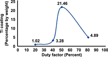
Figure 18. The relationship of duty factor (%) and percentage by weight of Ti coating (%). Reprinted from [45], Copyright 2012, with permission from Elsevier.
Download figure:
Standard image High-resolution imageIn the same year, another novel study on EDC process with PM electrode was conducted by Das and Misra [21]. They reported that an increase in duty factor is driven by the increase of pulse on time. They concluded that the average surface roughness, layer thickness and micro-hardness of coating all increase along with the duty factor. In addition, an increase in duty factor can trigger a spark erosion and form additional craters on the powder metallurgy electrode. This phenomenon also drives the transfer of material from the tool to workpiece surface as well as increases the MDR or MTR.
Moreover, the pin-on-disc reciprocating wear test carried out by Sharma et al [144] showed that the wear rate of the coated Ti alloy by hBN powder decreased as the duty factor increased from 0.3 to 0.7. This phenomenon was due to the rises in hardness of coated layer with duty factor. Based on their result, the minimum wear rate found for the coated Ti alloy was 0.05 mg min−1 whereas the Ti alloy substrate posed a higher wear rate of 0.22 mg min−1. Similarly, the value of CoF also rise with the duty factor due to the increase of discharge energy and caused the dissociation of hBN into BN. Nevertheless, the coated sample posed a lower CoF value of 0.26 compared to the Ti alloy substrate which posed a CoF value of 0.4.
However, the above finding contradicts the conclusions of Gill and Kumar [139], who discovered that as the duty factor increases, the surface of workpiece lacks enough idle time to cool down and interact with the deposited materials. Therefore, the alloyed material and suspense powder are flushed out from the workpiece surface by dielectric fluid. Subsequently, the micro-hardness of the coating decreases along with an increasing duty factor.
On the other hand, Tyagi et al [137] found that MoS2 + Cu coated surface morphology by PMEDM method was related to the duty factor. A very less deposition and high density of small pores surface was achieved with a low duty factor (30%). Conversely, a non-uniform surface with formation of voids and pores was achieved at a high duty factor (90%) due to the arcing process of the accumulation of fused material. Tyagi et al [137] explained that duty factor acted as kinetic and thermodynamic parameter that proportionally affected the coating processing rate. A coating surface quality degrade when the high duty factor is applied due to the debris does not flushed away and leads to the formation of irregular surface.
Figures 19 and 20 summarise the duty factor ranges used in previous EDC studies that employ the PMEDM and PM electrode methods, respectively.
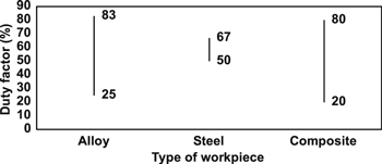
Figure 19. The range of duty factor used in EDC (PMEDM method).
Download figure:
Standard image High-resolution image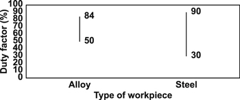
Figure 20. The range of duty factor used in EDC (powder metallurgical electrode method).
Download figure:
Standard image High-resolution image4.6. Polarity
The polarity of electrode and workpiece plays an important role in the workpiece surface modification. According to Das and Misra [21], the electrode used for surface modification by EDC can be either in positive or negative polarity, but its TWR must always be higher than its MRR. However, this theory does not fully explain the suitable polarity for the EDC process.
Vijayakumar et al [68] reported that EDC or EDA modifies the workpiece surface by applying reverse polarity (positive polarity). Polarity can be explained from the view point of current flow in a circuit. In the EDC process, the electrode is placed at the anode circuit (positive) due to anode circuit can melts faster than cathode (negative).
Bai and Koo [5] studied the effect of polarity on surface modification and found that the negative-polarity electrode was ineffective in the surface alloying process. The current or energy density of the cathode (negative terminal) is higher than that of the anode (positive terminal), but the discharge spot at the anode is larger than that at the cathode. The high discharge spot at the anode electrode creates a wide melting zone, whilst the high current at the cathode workpiece surface creates a deep molten zone. Therefore, the materials from the tool electrode and elements (C and oxygen) that are decomposed by dielectric fluid are successfully deposited on the workpiece surface.
The above argument has been supported by Krishna and Patowari [145], who found that positive polarity is suitable for the transfer of materials in the EDC process. They also revealed that a layer with high W and Cu concentrations was produced by using EDC with the reverse polarity (positive polarity) of the W–Cu PM electrode. The transfer of materials from the tool to the coated layer was confirmed by the results of the energy dispersive x-ray spectrum (EDX) analysis.
In 2016, Gill and Kumar [108] also identified positive polarity as an optimum parameter in their research. The coating produced by Cu–Mn powder metallurgy tool showed the best micro-hardness of 1191.7 HV, which was 93.7% higher than the micro-hardness of the H11 hot die steel base material (615 HV).
In sum, Das and Misra [21], Vijayakumar et al [68], Bai and Koo [5], Krishna and Patowari [145] and Gill and Kumar [108] all support the suitability of positive polarity for the EDC process.
4.7. Dielectric fluid
The literature has emphasised the importance of dielectric fluid to control the electrical discharge and thermal absorption during EDM process [146]. In EDC process, the presence of dielectric fluid mainly functions to transfer the suspended powder or eroded electrode material to the surface of workpiece and deposit on it [63, 142].
Kerosene oil or hydrocarbon oil is a very common and popular dielectric fluid that used to conduct EDC process for the surface modification of metal workpiece [43, 56, 61, 98, 143, 147]. Kerosene oil consists of a long hydrocarbon chain of C6–C16 and 150 °C–300°C of boiling point. However, EDM die sinker generates an extremely high spark temperature about 8000–12 000 °C [44], therefore the long hydrocarbon chain is decomposed and cause the release of C atom during EDC process [61, 148]. According to Hwang et al [43], the carbon atom released from kerosene oil plays a critical role in EDC process as it combines with the Ti atom in electrode to become a Ti–C and is coated on the surface of workpiece, resulting the increase of surface hardness and reducing the roughness and formation of micro-cracks. In the same vein, Janmanee and Muttamara [45] also claimed that the use of Ti powder mixed with kerosene oil can effectively increase the hardness of WC-Co workpiece from 990 HV to 1750 HV and simultaneously reduce the formation of voids and microcracks.
On the other hand, deionized water is commonly used as dielectric solvent in surface modification of β-phase Ti orthopaedic implant by PMEDM method [3, 125, 128]. Prakash et al stated that the deposition of bioceramic oxides (TiO2, Nb2O5, ZrO2, and SiO2) and carbide (TiC, SiC, and NbC) by PMEDM with deionized water provided an excellent metallurgical bonding with the β-phase Ti substrate and enhanced the biocompatibility of the implant surface with superior corrosion resistance [128]. Chen et al [125] discovered that the EDC process at the condition of peak current 0.1 A, pulse on time 30 μs and 50 μs and 6 g l−1 concentration of Ti powder mixed with deionized water able to enhance the hydrophilicity of the implant surface and reduce the formation micro-crack.
Besides, distilled water was also investigated and used in EDC process. In 2006, Bai and Khoo [5] compared the coating quality on superalloy Haynes 230 workpiece with kerosene oil and distilled water by using Al–Mo composite electrode. Based on their results, the maximum coating hardness produced with distilled water was higher than kerosene oil due to the excellent resolidification rate of distilled water. However, the coating produced with the kerosene oil caused the finest surface morphology, thicker coating layer and slowest oxidation rate when compared to all the experiment samples [5].
5. Characteristics of EDC coating
5.1. Surface roughness
Kalpakjian and Schmid [9] stated that the surfaces of different materials have a unique texture. Surface roughness can be defined as closely spaced, unequal deviations on a small scale and it also can be measured based on the height, width and distance along the surface. The arithmetic means value (Ra) is created from variety digitised data of a rough surface.
According to Yih-Fong and Fu-Chen [149], the surface roughness of the SKD11 workpiece is influenced by particle size of powder suspension in dielectric fluid. They found that the powder with the smallest particle size (70–80 nm) can be used to create the best surface finish. However, using a powder with a larger particle size will reduce the quality of the surface finish because a small powder particle size can produce a fine surface in a complementary manner. Figure 21 presents an optical microphotograph of the surface roughness of SKD 11 with different Al powder particle sizes under a constant experimental condition (duty factor = 67%, Ip =4 A, Ton = 25 μs and concentration = 0.5 cm3 l−1) and figure 22 shows the surface roughness result in different Al powder concentration, peak current and Al particle size.
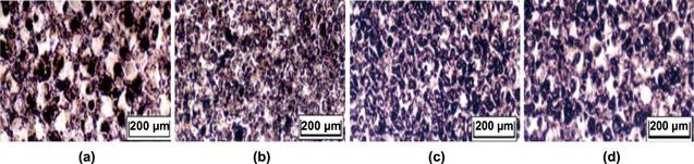
Figure 21. The optical microphotograph (a) without powder additives; (b) Al powder additives with size 70–80 nm; (c) Al powder additives with size 10–15 μm; (d) Al powder additives with size 100 μm. Reprinted from [149], Copyright 2005, with permission from Elsevier.
Download figure:
Standard image High-resolution image
Figure 22. Coating layer surface roughness versus concentration of aluminium powder for different peak current and aluminium particle size.
Download figure:
Standard image High-resolution imageThe findings of Yih-Fong and Fu-Chen are consistent with those of Bajaj et al [123], who found that the surface roughness decreases when an Si powder with a small particle size of 10–30 μm is used. However, Singh and his co-workers [107] challenged the conclusions of both Yih-Fong and Fu-Chen [149] and Bajaj et al [123] by arguing that increasing the powder size will reduce the surface roughness of the workpiece because a powder with a large particle size causes a less density powder particle in dielectric fluid. The large grain size of powder particles can easily enlarge and widen the discharge passage which easily flushed away by dielectric fluid. This phenomenon leads to a uniform dispersion of discharge energy in the machining area and the formation of shallow or small craters on the workpiece surface, thereby reducing surface roughness. Conversely, a small grain size of powder particles may enter the spark gap and clogs the discharge passage. This phenomenon leads to short circuit, instable process and causes the black carbon layer deposited on both the surface of electrode and workpiece resulting in a high value of surface roughness. Figure 23 illustrates the result of surface roughness versus the grain size from the research of Singh and his co-workers [107].
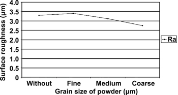
Figure 23. Surface roughness versus grain size. Reproduced with permission from [107].
Download figure:
Standard image High-resolution imageIn 2015, Mussada and Patowari [113] highlighted the importance of surface roughness in determining the topographical status of a deposited surface. Specifically, the value of surface roughness can influence the performance and value of the finished product. This value obviously increases along with pulse on time and current but only slightly increases along with compact load. Two years later, Mussada and Patowari [114] argued that measuring surface roughness is very important in determining the structural status of the material deposited layer. The value of surface roughness can be measured by using the Handysurf E-35A surface roughness profilometer. The original workpiece has an average roughness of 13.3 μm, maximum roughness (Rzmax) of 62.9 μm, and mean spacing (RSm) of 298.90 μm. After a 5 min machining with 106 μs pulse on time and 10 A peak current, the Ra, Rzmax and RSm have been reduced to 8.3, 48.4 and 174.24 μm, respectively. The roughness profile measurement after the machining shows that the decreases of surface roughness value lead to the smoothest workpiece surface.
In addition, Gill and Kumar [139] observed that the workpiece discharges more molten material from the crater at a higher peak current, thereby increasing the value of surface roughness. However, no microcracks are observed on the workpiece surface when PM electrodes are used. In this case, they confirmed that the alloying process does not affect the machining surface. Similar to Rahang and Patowari [115], they also agreed that the an increase in surface roughness can be ascribed to the increase in peak current setting. Specifically, a high peak current setting will lead to a non-uniform deposition on the workpiece surface. Furthermore, Ahmed [24] discovered that a current setting of 6 A can achieve the highest surface roughness of 9.5 μm Ra whilst a current setting of 3 A can lead to the lowest surface roughness, thereby proving that the surface roughness of the workpiece increases along with the peak current setting. Table 11 summarises the surface roughness of the workpiece before and after the EDC process as revealed in previous studies.
Table 11. Summary of surface roughness before and after EDC process.
| Surface Roughness (μm) | |||||
|---|---|---|---|---|---|
| Workpiece | Electrode | Method | Before | After | References |
| Aluminium | TiC–Cu | PM electrode | — | 5.35–9.08 | [21] |
| Super Co 605 | Graphite | PMEDM | 2.23 | 1.99 | [66] |
| Ti30Ta | Pure Ti | PMEDM | 2.4 | 2.1 | [118] |
| AISI-D2 die steel | Cu | PMEDM | 1.2 | 0.4 | [130] |
| 45# carbon steel | Ti | PMEDM | 5.32 | 4.55 | [150] |
| SiCp/Al | Cu | PMEDM | 0.834 | 0.571 | [151] |
5.2. Layer composition
Mussada and Patowari [19] performed an x-ray diffraction (XRD) analysis to examine the elements deposited on the Al workpiece surface. As their result, tungsten (W), copper (Cu) and carbon (C) were found on the surface of Al workpiece. The XRD profiles identify Cu and W as the primary elements on the workpiece surface given that these elements are the material deposits from the W–Cu PM electrode. Meanwhile, the presence of C on the workpiece surface can be ascribed to the C elements decomposed from the hydrocarbon oil dielectric fluid, thereby forming WC on the Al workpiece surface. Figure 24 shows the XRD profiles.
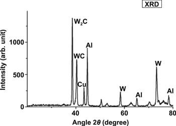
Figure 24. The XRD profiles. [19], 2015, reprinted by permission of the publisher (Taylor & Francis Ltd).
Download figure:
Standard image High-resolution imageIn his quantitative elemental investigation, Ahmed [24] found that EDX can reveal the movement of materials transfer from the electrode to the workpiece surface. The presence of Ti, boron (B) and C in the EDX profiles confirms the migration of materials from the Ti–B4C PM electrode to the Al workpiece [24].
In 2017, Prakash and Uddin [3] found that the composite elements on the workpiece surface after EDC or EDA can be observed by using XRD. They mixed HA powder with deionised water as dielectric fluid and then determined the deposited material on the surface via XRD (X'pert-PRO) with CuKα radiation at 45 kV, 40 mA and incident angle of 2θ. They found that the elements on the surface of the β-Ti implant after the EDC or EDA process include Ti, Nb, Ta, Zr, O, Ca and P, which formed biocompatible phases, such as Ca3(PO4)2, CaZrO3, Nb8P5, CaO, TiP, Nb4O5, TiO2 and TiH. They ascribed the presence of Ti, Nb, Ta and Zr elements to the base material (β-Ti implant) and the presence of O, Ca and P elements to the decomposition of HA powder in the dielectric fluid. In the same year, Chakraborty et al [98] argued that the movement of materials transfer from the SiC–Cu electrode to the Al workpiece surface. Figure 25 shows the microscopic image of the deposited layer on the workpiece surface. By performing an XRD analysis, they observed Si, SiC, and Cu elements deposited on the Al workpiece surface, thereby confirming the transfer of materials (in the form of elements and carbides (SiC)) from the electrode to the workpiece surface.

Figure 25. The microscopic images. (a) The deposited layer using 20 Ton SiC30:Cu70 compact tool; (b) the deposited layer using 15 Ton SiC50:Cu50 compact tool; (c) the parent material, interface and deposited layer. Reproduced with permission from [98].
Download figure:
Standard image High-resolution image5.3. Layer thickness
According to Prakash and Uddin [3], deposited layer thickness refers to the depth of the deposited surface after the EDC process. Layer thickness can be measured by observing the test specimen with a cross-sectional morphology. By applying an adequate polishing method to prepare the test specimen, Prakash and Uddin obtained an 18–20 μm thick deposited layer that contained biocompatible phases. The base material has generated a metallurgical bonding with the deposited layer and formed a mechanical interlock between the base material and deposited material. Figure 26 presents the micrograph of the cross-sectional deposited layer.

Figure 26. Micrograph of cross-sectional deposited layer. Reprinted from [3], Copyright 2017, with permission from Elsevier.
Download figure:
Standard image High-resolution imageMeanwhile, Ahmed [24] achieved a deposited layer thickness of approximately 22.4 μm. As can be seen in the SEM micrograph, this deposited layer has a uniform thickness and has been well deposited on the surface of the base material. Figure 27 shows the SEM micrograph of the cross-section of the base material and deposited layer.
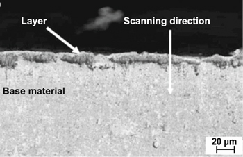
Figure 27. The SEM micrograph of the cross-section of base material and deposited layer. [24], 2016, reprinted by permission of the publisher.
Download figure:
Standard image High-resolution imageChen et al [125] found that the coating layer thickness increases along with the concentration of Ti powder in dielectric fluid. Specifically, they revealed that the thickness of the Ti implant recast layer ranges from approximately 3–10 μm with a 3 g l−1 concentration of Ti powder. However, the thickness of the deposited layer increases from 4 to 11 μm when the concentration of the Ti powder increases to 6 g l−1. In a same vein, Kolli and Kumar [122] found that the dielectric fluid with l g/l B4C powder achieves a lower layer thickness compared with the dielectric fluid with 15 g l−1 B4C powder.
Furthermore, Chakraborty et al [98] revealed that deposited layer thickness increases proportionally along with the current and pulse duration. This finding has been supported by Rahang and Patowari [115], who achieved deposited layer thicknesses of 185 μm and 24 μm at high and low currents and pulses on time, respectively. However, these findings contradict the conclusions of Sahu et al [26], who argued that the thickness of the coating layer decreases and a non-uniform deposition is formed along with an increasing duty factor and pulse on time because such increase triggers a non-uniform material deposition from the PM electrode to the workpiece surface. In addition, they found that the thickness of the coating layer increases along with the discharge current due to the increase in the MDR and TWR of the PM electrode. Table 12 summarises the coating layer thickness reported in previous research.
Table 12. Summary of coating layer thickness obtained after EDC process.
| Workpiece | Electrode | Method | Coting layer thickness (μm) | References |
|---|---|---|---|---|
| β-Ti alloy | Pure Ti | PMEDM | 18–20 | [3] |
| Aluminium | TiC–Cu | PM electrode | 30.11–60.34 | [21] |
| Aluminium | Ti–B4C–Al | PM electrode | 22.4 | [24] |
| AISI 1040 stainless steel | TIC–Cu | PM electrode | 46–112 | [26] |
| WC-Co | Cu | PMEDM | 5 | [45] |
| 45# carbon steel | Ti | PMEDM | 15 | [53] |
| 304 stainless steel | TiC and Cu | PMEDM | About 8 | [65] |
| Aluminium | SiC–Cu | PM electrode | 44.01–83.644 | [98] |
| Alloy tool SKD11 steel | Cu | PMEDM | 3 | [99] |
| Aluminium | Ti | Dry EDC | 20 | [100] |
| Ti30Ta | Pure Ti | PMEDM | About 9 | [118] |
| Ti–6Al–4V | Cu | PMEDM | 13.3 | [122] |
| 304 stainless steel | Ti–C | PM electrode | About 10 | [74] |
| 45# carbon steel | Ti | PMEDM | 25 | [150] |
| 70Ti–Ta30 | Ti | PMEDM | 7 | [152] |
| Ti–6Al–4V | Cu | PMEDM | 12–18 | [153] |
5.4. Micro-hardness
Prakash and Uddin [3] applied the Vickers hardness test to measure the micro-hardness of the deposited surface and found that the micro-hardness of the β-Ti implant substrate increases from 390 HV to 1275 HV along with the deposition of the HA-containing bioceramic layer and demonstrates a perfect adhesion strength.
Janmanee and Muttamara [45] argued that when a high temperature is applied, the solidifying rate of the Ti powder suspension in the dielectric fluid increases and creates a 5 μm thick layer on the surface of the WC workpiece. Their experiment results reveal a Ti–C deposition on the workpiece surface with a micro-hardness of 1750 HV, which is about 1.75 times (76.76%) higher than that of the base material (998 HV). Figure 28 shows the micro-hardness (HV) against the depth of surface (μm) and the distribution of micro-hardness for a cross section of workpiece.
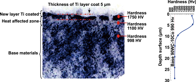
Figure 28. The distribution of micro-hardness for a cross section of workpiece. Reprinted from [45], Copyright 2012, with permission from Elsevier.
Download figure:
Standard image High-resolution imageIn another major study, Gill and Kumar [139] and Li et al [153] found that the micro-hardness of the deposited layer is always higher than that of the base material because of the presence of C particles and cementite. During the EDC process, C decomposes from the dielectric fluid and deposits on the workpiece surface, thereby creating a crack-free surface as a result of the alloying mechanism applied on this surface.
The increase in coating hardness after the EDC process can also be ascribed to the extremely rapid cooling process. Ou and Wang [152] found that the coating layer comprises elements from the dielectric fluid and suspended powders or materials from the tool and workpiece. These materials are transferred to the workpiece surface via electrical discharge and then undergo an extremely rapid cooling process before they are solidified and deposited on the workpiece surface. Such extremely rapid cooling process may also explain why the micro-hardness of the coating is higher than that of the original workpiece. However, Rahang and Patowari [115] stated that the increase in micro-hardness can be ascribed to the migration of electrode materials (W and Cu) to the base material (aluminium). The micro-hardness of the deposited layer ranges from 328 HV to 370 HV, whilst that of the base aluminium material only ranges from 97.7 HV to 104 HV. Ahmed [24] also observed that the average and highest micro-hardness of the deposited layer can reach as high as 640 HV and 754 HV, respectively, which are three times higher than the micro-hardness of the origin base material. Figure 29 shows the microhardness along the cross-sectional of the test specimen, whereas table 13 summarises the workpiece micro-hardness before and after the EDC process as reported in previous studies.
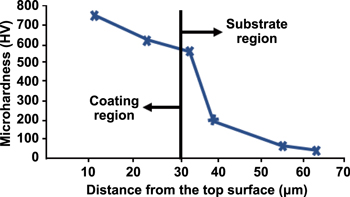
Figure 29. The microhardness along the cross-sectional of the test specimen. [24], 2016, reprinted by permission of the publisher (Taylor & Francis Ltd).
Download figure:
Standard image High-resolution imageTable 13. Summary of micro-hardness before and after EDC process.
| Micro-hardness (HV) | |||||
|---|---|---|---|---|---|
| Workpiece | Electrode | Method | Before | After | References |
| β-Ti alloy | Pure Ti | PMEDM | 400 | 1275 | [3] |
| Aluminium | TiC–Cu | PM electrode | 140–155 | 1183–1929 | [21] |
| 304 stainless steel | TiC | PM electrode | 196 | 1888 | [22] |
| Mild steel | W–Cu | PM electrode | 332–350 | 879.8–1367.22 | [25] |
| AISI 1040 stainless steel | TIC–Cu | PM electrode | 201 | 350–450 | [26] |
| WC-Co | Cu | PMEDM | 990 | 1750 | [45] |
| 45# carbon steel | Ti | PMEDM | 200 | 1780 | [53] |
| Aluminium | Cu | PMEDM | 106.67 | 218.33 | [61] |
| Super Co 605 | Graphite | PMEDM | 320.82 | 1315.2 | [66] |
| Aluminium | SiC–Cu | PM electrode | 95 | 149.03–301.05 | [98] |
| Alloy tool SKD11 steel | Cu | PMEDM | 653 | 1100 | [99] |
| Aluminium | W–Cu | PM electrode | 97.9–104 | 328–370 | [115] |
| AISI-D2 die steel | — | PMEDM | 275 | 982 | [117] |
| Ti–6Al–4V | Cu | PMEDM | 339 | 1110 | [71] |
| AISI 1049 carbon steel | Cu | PMEDM | 1360 | 1600 | [131] |
| 45# carbon steel | Ti | PMEDM | 300 | 1420 | [150] |
| SiCp/Al | Cu | PMEDM | 200 | 325 | [151] |
| Ti–6Al–4V | Cu | PMEDM | 310 | 630 | [153] |
5.5. Tool wear rate
The tool wear of electrode can be defined as a corrosive wear resulting from the chemical and electrochemical reactions between the surface and the environment. When the corrosion layer is demolished, an alternative layer is formed and the corrosive layer formation is repeated [9]. The TWR of the EDC process has been examined in only few studies, including Kolli and Kumar [154] and Marashi et al [41].
Kolli and Kumar [154] argued that TWR is influenced by the concentration of B4C powder used for the PMEDM process. TWR increases as the concentration of B4C powder increases from 1 to 15 g l−1. This powder has excellent chemical, physical, wear and abrasion resistance, high thermal fusion and low thermal expansion. Increasing the concentration of B4C powder also increases the thermal and electrical conductivity of dielectric fluid, thereby accelerating the discharge of transitivity of the plasma channel and sparking frequency, respectively, and flushing away debris from the gap between the electrode and workpiece.
Marashi et al [41] highlighted TWR as another important parameter that reduces the efficiency of the EDC process, increases the tool costs and affects the accuracy of the results. TWR can be explained by the reduction in the weight and volume of the electrode along with increasing machining time. Chakraborty et al [98] performed an experiment on TWR by using the green compact electrode method and found that in the EDC process, the TWR decreases along with an increasing electrode compact load. Meanwhile, when the current increases, the support energy increases to the point of discharge. This cause the TWR increases and creates a less dense and porous electrode at the same time.
Moreover, Das and Jain [138] reported that the increases of peak current and pulse on time lead to the rises of TWR. As the peak current increases from 4 to 10 A and pulse on time increases from 60 to 260 μs, the amount of spark erosion increases and causes the crater form on the surface of electrode. However, this phenomenon simultaneously enhanced the material deposition rate from the TiC–Cu green compact electrode to the surface of aluminium workpiece. These results are in agreement with Ahmed's findings [24] which showed that with the increase in peak current, more material from the Ti–B4C PM electrode melts due to more sparks generated between the gap of electrode and surface of workpiece and lead to the increase of TWR.
5.6. Corrosion resistance
A significant analysis and discussion on the corrosion resistant was presented by Toshimitsu and his co-worker [99]. They reported corrosion test can be analysed by using the electrochemical analysis system as shown in figure 30. In this system, the NaCl solution is used as dielectric fluid, the SKD11 workpiece after the EDC process acts as the work electrode, Ag/AgCl is used as the reference electrode and platinum acts as the counter electrode due to its inert properties. Platinum only acts as a conductor and does not undergo any chemical reaction [155]. In the end of their research, they found that SKD11 surface with chromium powder additives show a better corrosion resistance compared with the SKD11 surface that did not undergo the EDC process.
Figure 30. The illustration of electrochemical analysis system. Reprinted from [99], Copyright 2016, with permission from Elsevier.
Download figure:
Standard image High-resolution imageSumi et al [156] performed an aqua regia dip test to investigate the corrosion resistance of the SUS316 workpiece with a one-hour dip time. The workpiece with the Si-containing amorphous coating layer is not corroded, but the area without such coating is corroded by 0.15 mm. During the test, bubbles are formed in the area without coating, but no bubbles have been formed in the area with coating. The SEM micrographs reveal an exposed grain boundary on the workpiece surface without coating but do not show any signs of damage on the coated surface, thereby proving that EDC can improve the corrosion resistance of the workpiece by depositing a layer of coating. These results are similar to those reported by Sharma et al [144]. The corrosion test carried out by Sharma et al [144] were on both the basis of flowing and stagnant water type condition, the corrosion rate of the coated and uncoated Ti alloy by hBN PMEDM method were compared. Based on their results, the corrosion test in stagnant water showed that the corrosion rate decreases from 4.89 μm yr−1 (Ti alloy substrate) to 1.07 μm yr−1 for the coated sample as the rises of hBN powder concentration in dielectric fluid. Similarly, the corrosion test in flowing water showed that the corrosion rate decreases from 5.92 μm yr−1 (Ti alloy substrate) to 1.24 μm yr−1 for the coated samples. These phenomena occurred due to the low pores density when a high hBN powder concentration was used, which reduced the opportunity of direct contact between the Ti alloy substrate and the NaCl solution through the pores and simultaneously reduce the corrosion rate.
Apart from that, Prakash et al [128] also discovered that the bioceramic-oxide deposited layer has excellent corrosion resistance and can act as a barrier to prevent corrosion when the implant surface is exposed to a corrosive environment. They found that PMEDM not only enhances the micro-hardness of the implant surface but also increases its corrosion resistance. These findings have been supported by Prakash and Uddin [3], who found that the coated layer (bioceramic layer) has a higher corrosion resistance (0.000 15 mm yr−1 of corrosion rate) than the base material (β-Ti implant; 0.0070 mm yr−1 of corrosion rate) under a simulated body fluid solution. The corrosion resistance of the base material is improved by a deposited layer, which acts as a protective layer when the base material is exposed to a corrosive environment. The EDC process produces a thick bioceramic layer with a nano-texture that prevents the base material from corroding and promotes bone-in-growth.
5.7. Wear resistance
The EDC process can enhance the wear resistance of the workpiece by applying the suitable parameters. Hu et al [151] examined the wear resistance of SiC-particle-reinforced Al matrix composites by using HIT friction and wear tester as well as by comparing the surface trade and wear mass. The wear mass of the original workpiece surface (about 10 mg) is about 10 times higher than that of the surface after the PMEDM process (about 1 mg). Therefore, the PMEDM process can efficiently improve the surface wear resistance of SiC-particle-reinforced Al matrix composites.
Besides, Ueno et al [147] claimed that the EDC process can improve the wear resistance of rolls by using a TiC sintered electrode. The EDC parameter plays a very important role in achieving a high wear resistance and defect-free TiC coating on the roll surface. They found that the wear resistance of rolls deposited with TiC via EDC is higher than that of conventional chrome-plated rolls. These findings are similar to those of Tijo and Masanta [71], who reported an improvement in the wear resistance of a Ti–6Al–4 V alloy workpiece coated with TiC–TiB2. This coating has a wear rate ranging from 3 × 10⁻⁵ to 11 × 10−5 g min−1, which is 2–7 times lower than that of the base material (22 × 10−5 g min−1).
A recent study by Algodi et al [157] discovered that the wear resistance of high-speed steel and 304 stainless steel can be improved by depositing a layer of TiC/Fe cermet via EDC with a semi-sintered TiC electrode. The wear performance of the workpiece increases as the TiC/Fe cermet creates graded equiaxed and banded columnar grains on the interface between the workpiece and coating. In the same year, Algodi et al [74] also claimed that 304 stainless steel workpieces with TiC–Fe coating have wear rates that are two orders of magnitude lower than those of the original 304 stainless steel workpieces after the EDC process.
Murray and Clare [101] conducted a ball-on-flat reciprocal wear test on the samples produced by EDC process with TiC, Si and Cu electrodes. Based on their results, the TiC coating caused the lowest CoF, which was about 0.2–0.3 and the friction results did not rise with time. Moreover, the samples produced by Cu electrode caused a better wear resistance compared to Si coating and surface of substrate despite the Cu only shown 1.07% on the surface. This result suggested that EDM die sinker was able to generate a high wear resistance surface.
On the other hand, Sharma et al [144] carried out pin-on-disc wear tests of the surface of Ti alloy which was coated by using hBN PMEDM method. The pin-on-disc wear test was conducted at a constant 400 rpm wear disc, 1 kgf dead load and 5 min wear duration. The wear test results discovered that coating layer posed a high wear resistance with a minimum wear rate 0.05 mg min−1 and 0.26 of CoF compared to the Ti alloy substrate (0.22 mg min−1 of high wear rate and 0.40 of CoF). This indicated that the EDC process significantly enhanced the wear and friction of Ti alloy substrate by coating a layer on it.
6. Applications of EDC
Many surface modification technologies are being applied nowadays, including carburising, electroplating, physical vapour deposition and plasma spraying [9]. Although the EDC process is still not widely being used by industries, many studies have highlighted its many functions for different sectors and applications.
6.1. Industrial applications
EDC can modify the surface of various manufacturing equipment, including moulds, dies and drills [158, 159], to prevent the defects as shown in figure 31 [160]. This approach is also suitable for industrial applications due to its ability to enhance the characteristics of the original surface of equipment in terms of corrosion and wear without a direct contact between the electrode and workpiece [27, 68]. EDC also can reduce the formation of chatter, mechanical stress and vibration during the process [68, 161].

Figure 31. Defects of die and molds. Reproduced with permission from [160].
Download figure:
Standard image High-resolution imageIn the previous study of material deposition process, Mussada and Patowari [114], Chen and Wu [29] and Madhaw [25] reported that that most of the existing surface modification technologies require an inert atmosphere, whereas EDC does not require the coating environment to be inert. Instead, by using a suitable controlling parameter, EDC can modify the workpiece surface by depositing a thick or thin layer of material [63].
Meanwhile, Mussada and Patowari [19], Tijo [27] and Bröcking et al [136] found that EDC can be used for roll texturing and roll recovery by improving the wear resistance of the material. This process is usually performed for stainless-steel strip manufacturing and can be used to increase the hardness, CoF, performance and lifespan of rolls [162].
Chen et al [133] argued that EDC can be used to repair the worn region of workpieces by coating them with a protective layer. This finding has been supported by Janmanee and Muttamara [45] in 2012. EDC has been introduced with an aim to modify the surface of tools to extend their lifespan and reduce their manufacturing costs [45, 58, 140].
In sum, EDC process is a crucial and effective method to enhance the surface properties and enable functionalization of materials for industrial applications. For example, EDC process successfully enhanced the surface properties of roll textures in terms of reducing the surface roughness [42, 136] and increased the surface hardness [42, 158], resulting in the increase of roll wear resistance [42]. Moreover, molds and dies used in the industry also can be functionalized by using EDC process, which are able to increase the life span and durability by increasing the micro-hardness [61], corrosion resistance [100] and wear resistance [144].
6.2. Biomedical applications
Chen and his co-worker [125] found that most studies on surface modification only focused on the application of a thick and porous oxide layer on the medical Ti implant surface to enhance the growth of tissues and accelerate healing. However, oxide layers can degrade in time due to the cleaning process and friction. The metal implant surface will corrode also given that body fluids contain amino acids and proteins [163]. By contrast, the EDC process has great potential to functionalise the surface with oxide layers. Similarly, Sales et al [164] revealed that EDC can be used for biomedical applications, such as improving the biocompatibility of the Ti6Al4V alloy to human bone and teeth by depositing a layer of Ti perovskite (CaTiO3). Figure 32 shows the artificial cell that attached and grew on EDC treated and untreated surface.
Figure 32. Human bone cells attachment on the untreated, EDM treated (Ip = 5 A), EDM treated (Ip = 10 A), and , EDM treated (Ip = 15 A) surface at (A) day 1 and (B) day 7. Reproduced with permission from [165].
Download figure:
Standard image High-resolution imageThe other applications of EDC have been studied by Prakash and Uddin [3], Aliyu et al [120], Abdul Rani et al [129] and Prakash et al [128]. All of them claimed that mixing EDC with a suitable powder alloy can enhance the corrosion resistance of the β-phase Ti alloy, which is widely used for orthopaedic and dental implants. This process can provide surface functionalization for cellular bioactivity, which enhances cell attachment, promotes the proliferation of cells and increases the DNA content. Figure 33 presents the image of artificial hip joint and the corrosion happen after implantation.
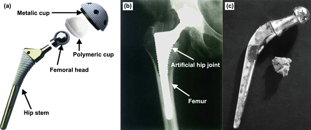
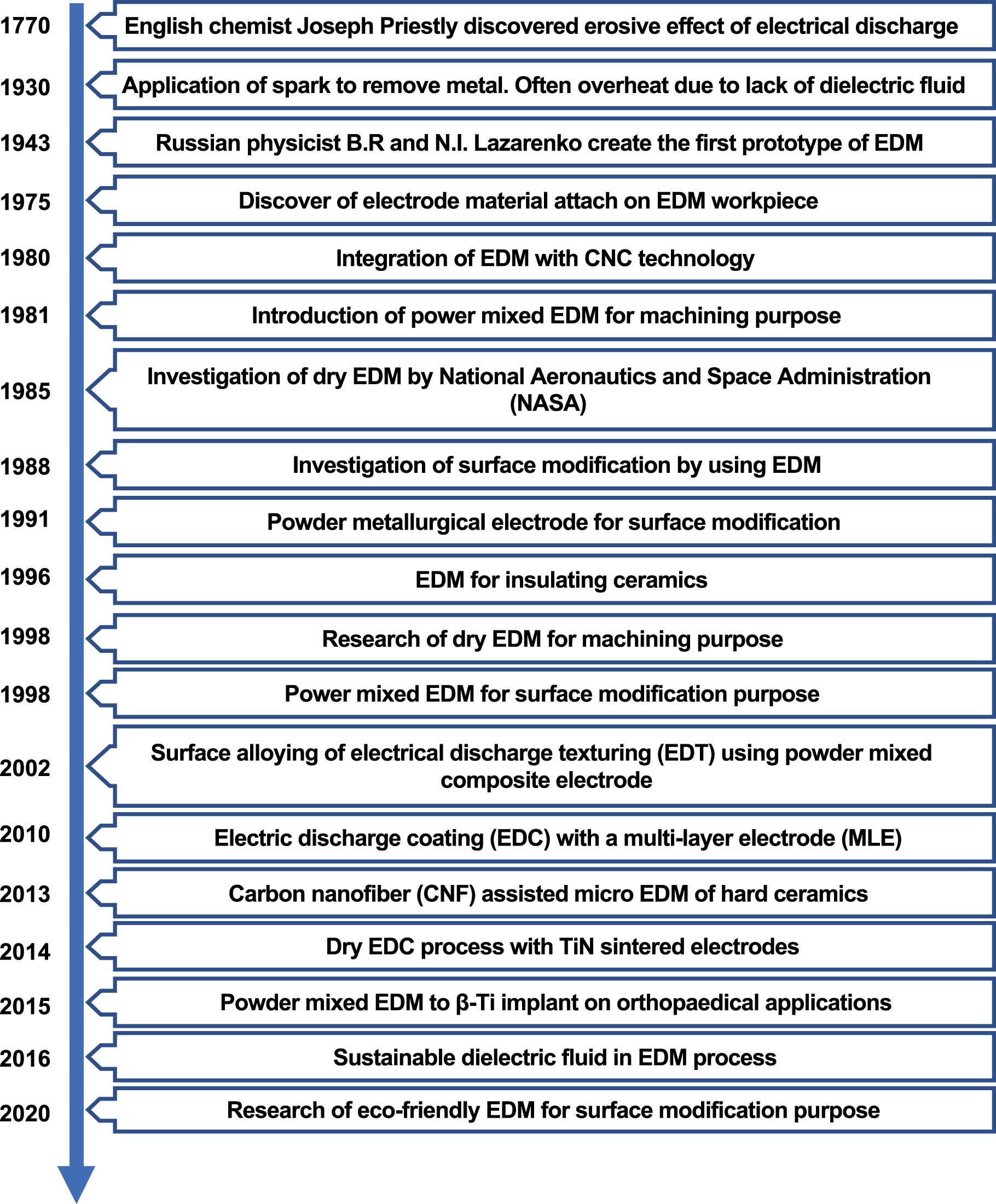
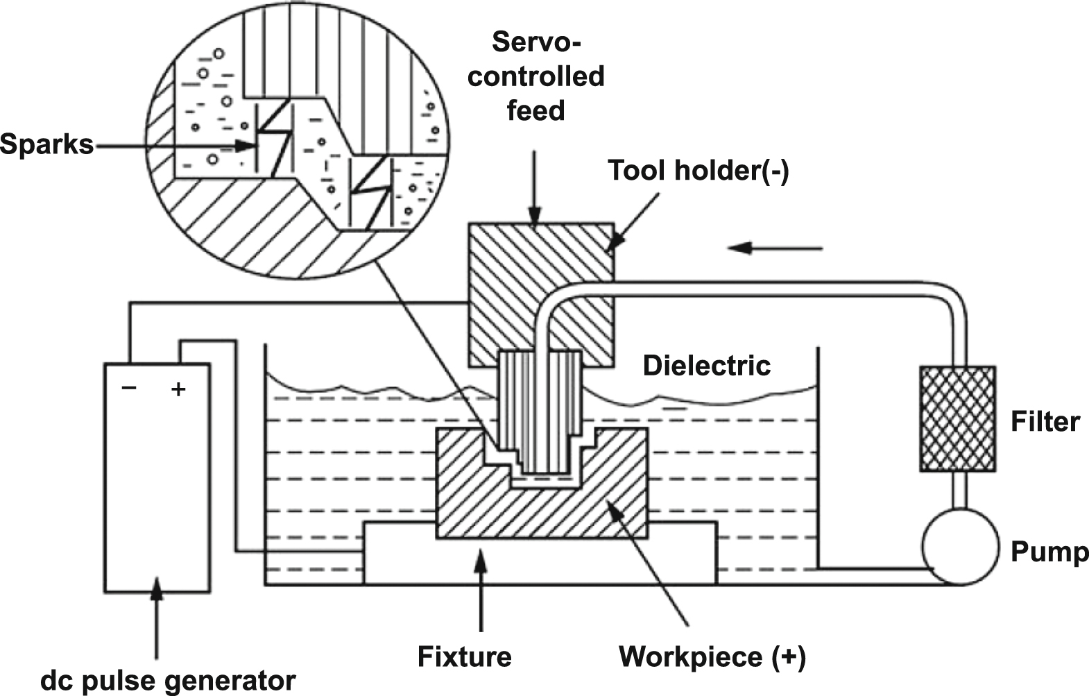
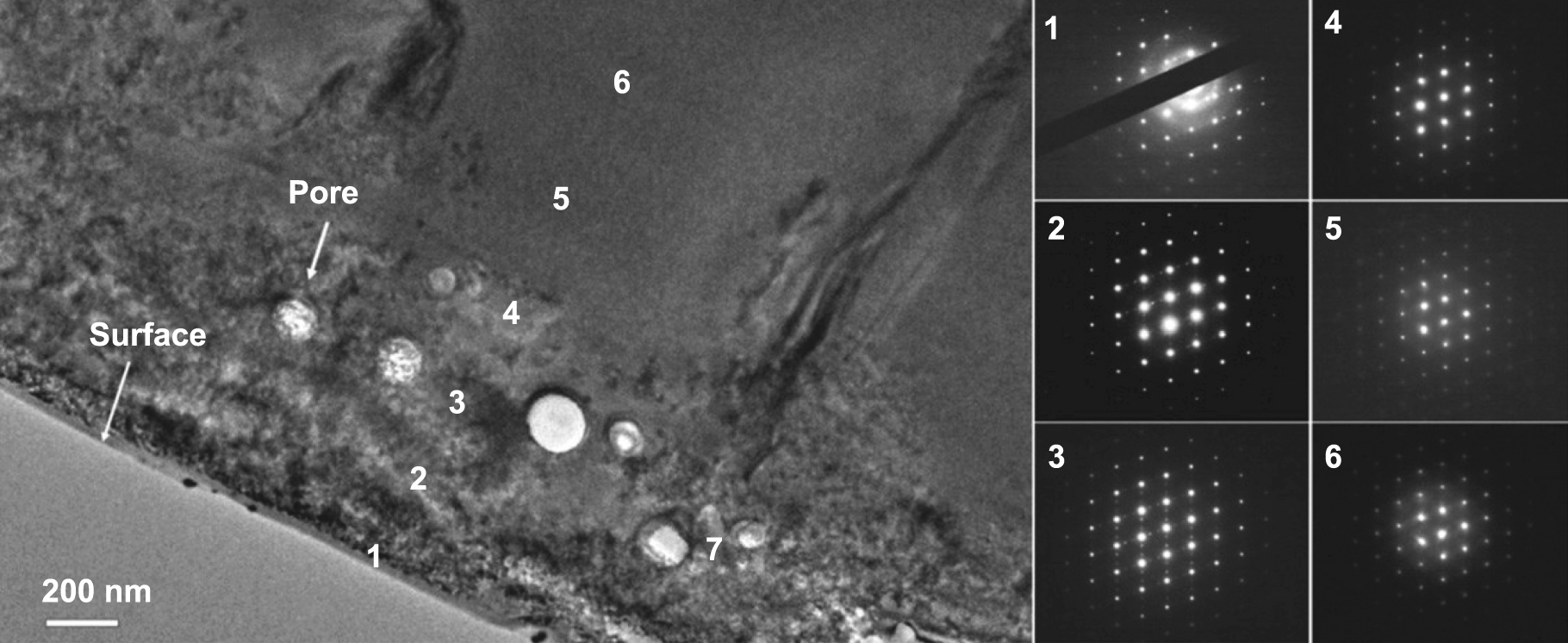
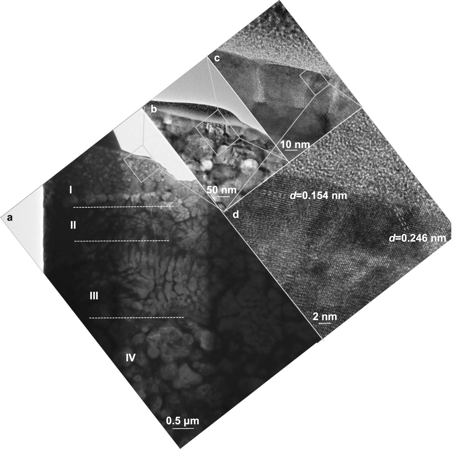
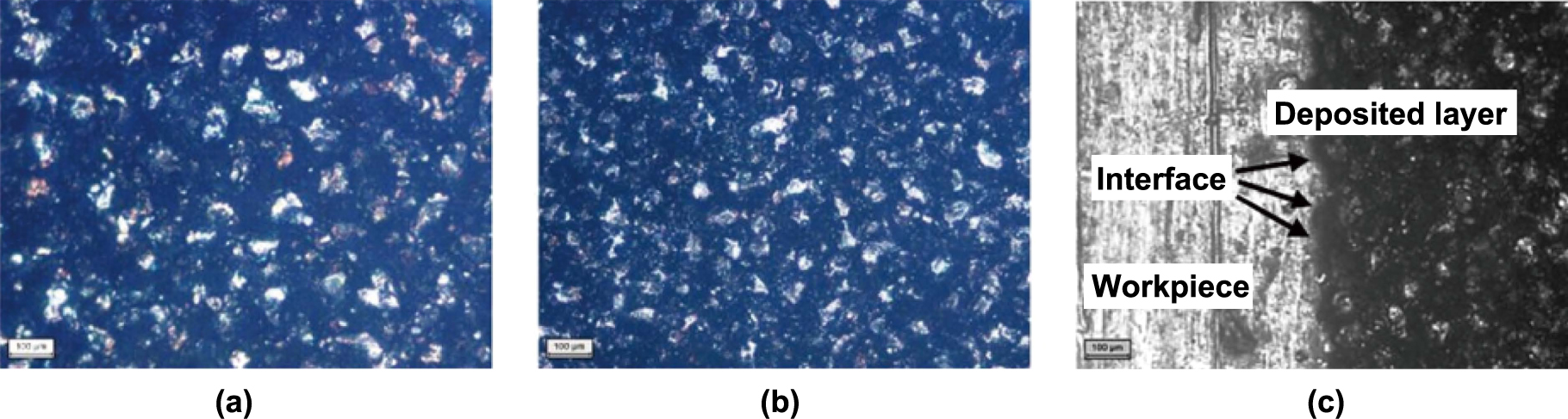
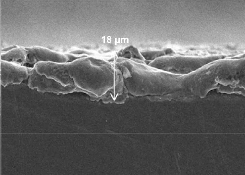
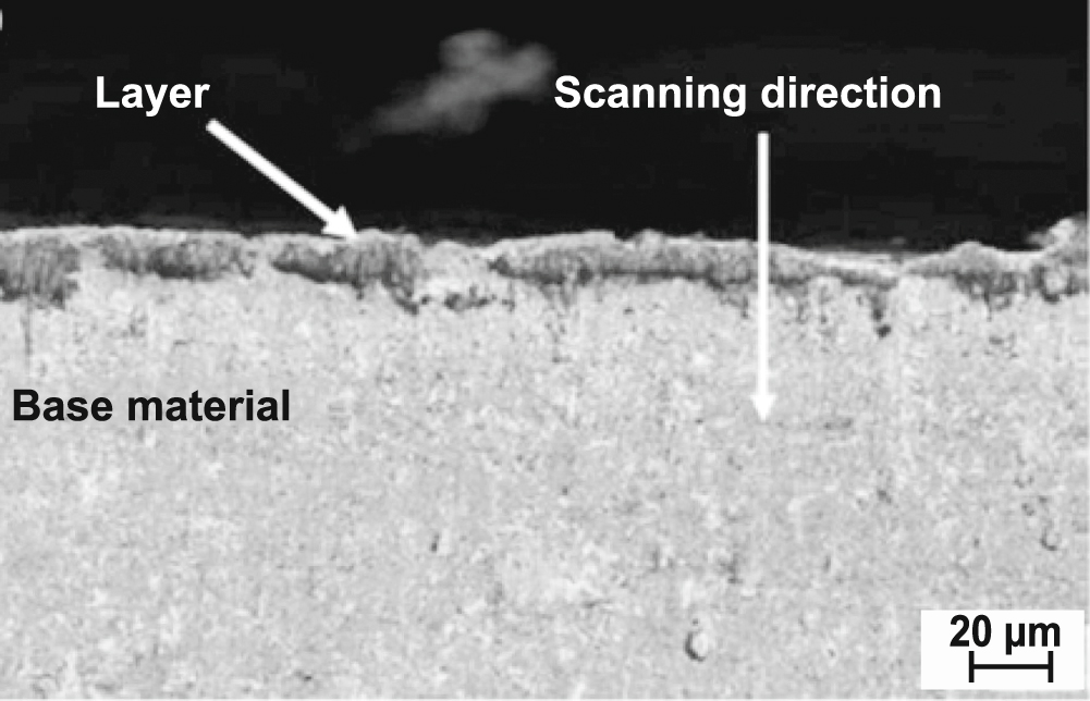
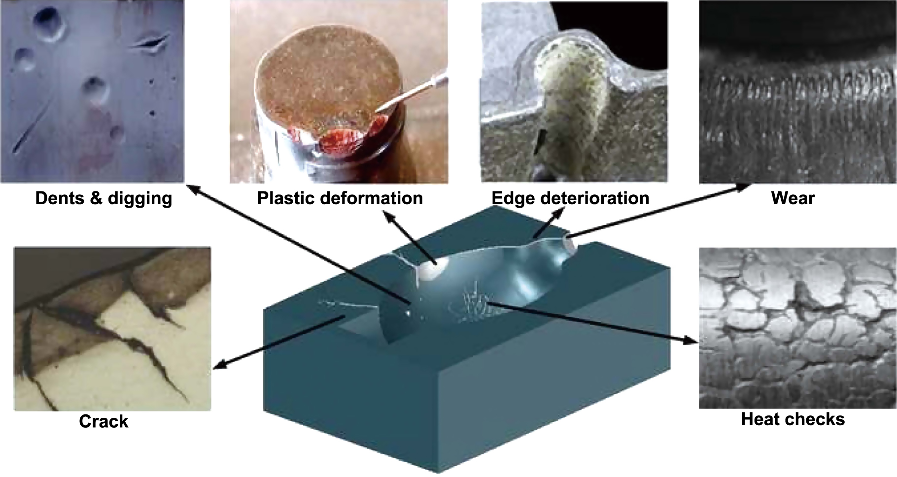
Figure 33. Artificial hip joint: (a) structure, (b) implanted into human body, (c) corroded after implantation. Reprinted from [166, 167], Copyright (a) 2004, (b), (c) 1998, with permission from Elsevier.
Download figure:
Standard image High-resolution image
In short, the EDC process has a great contribution for the material surface modification and functionalization for biomedical applications [120, 125, 164]. By using the EDC process, the biocompatibility of the artificial implants can be improved with the cells attachment and proliferation [128, 165].
7. Summary
This paper reviewed the previous research on surface modification via EDC technology. The methodologies, parameters and characteristics of various EDC processes for various materials were discussed and compared. The literature review has demonstrated that the PMEDM and PM electrode methods are effective solutions for realising EDC. These processes have the following key features:
- Reverse polarity (electrode positive polarity) is more suitable for EDC process compare to straight polarity (electrode negative polarity).
- The addition of powder in dielectric fluid can enhance the coating quality and reduce defect such as micro-holes.
- The concentration and particle size of the powder used in PMEDM have significant effects on the coating surface.
- The dry EDC process can reduce the use of dielectric fluid and overcome environmental pollution problems.
- The compact load of the PM electrode has a significant effect on the TWR and layer thickness.
- Peak current and pulse on time are the most significant parameters for controlling TWR, surface roughness, layer thickness and MTR.
8. Future trends
The EDC process brings many advantages in enhancing the surface properties and creating surface functions of metal and other materials. In addition, EDC is cheaper and more effective compared with the other extant coating processes. This technology is expected to be used in automotive, aerospace and maritime industries for surface modification and restoration purposes, particularly for engine pistons, jet turbines and marine propellers. It is also expected to be widely used in biomedical applications. However, EDC is not completely free from pollution given its use of dielectric fluid and its creation of a by-product. Therefore, future research should examine the environmental aspects of the EDC process and develop EDC processes for surface modification at an eco-friendly manner. Efforts should also be made to identify the optimum parameters that can produce a defect-free coating with controllable surface topography and roughness.
Acknowledgments
Pay Jun Liew and Ching Yee Yap acknowledge the supports from Universiti Teknikal Malaysia Melaka (UTeM) for the technical and financial supports through the grant PJP/2018/FKP(6A)/S01587.
Conflict of interest
The authors declare that there is no conflict of interest regarding the publication of this paper.