
Abstract
This review focuses on recent developments in additive manufacturing (AM) of precision optical devices, particularly devices consisting of components with critical features at the micro- and nanoscale. These include, but are not limited to, microlenses, diffractive optical elements, and photonic devices. However, optical devices with large-size lenses and mirrors are not specifically included as this technology has not demonstrated feasibilities in that category. The review is roughly divided into two slightly separated topics, the first on meso- and microoptics and the second on optics with nanoscale features. Although AM of precision optics is still in its infancy with many unanswered questions, the references cited on this exciting topic demonstrate an enabling technology with almost unlimited possibilities. There are many high quality reviews of AM processes of non-optical components, hence they are not the focus of this review. The main purpose of this review is to start a conversion on optical fabrication based on information about 3D AM methods that has been made available to date, with an ultimate long-term goal of establishing new optical manufacturing methods that are low cost and highly precise with extreme flexibility.
Export citation and abstract BibTeX RIS

Original content from this work may be used under the terms of the Creative Commons Attribution 3.0 licence. Any further distribution of this work must maintain attribution to the author(s) and the title of the work, journal citation and DOI.
1. Introduction
Manufacturing techniques are often classified into subtractive and additive methods or, in some cases, a combination of the two methods [1]. Subtractive techniques are based on material removal. In an additive manufacturing (AM) process, however, the workpiece is fabricated point by point or layer by layer from a computer-aided design file [2]. Thanks to advancements in this technology, the number of printable materials by AM has increased enormously, including metals [3], polymers [4], and ceramics [5]. Since AM can offer more flexibility in the design and manufacturing of complex-shaped components, its implementation in areas such as microfluidics and nanoelectronics [6], aerospace [7], tissue engineering [8], and medicine [9] is becoming increasingly popular.
In optical manufacturing, AM, as an advanced manufacturing method, has been gaining interest because of its capabilities in the fabrication of extremely complex shapes. It features multiple-scale levels in one setting, which was quite difficult in the past using traditional fabrication methods, such as precision machining [10], precision compression molding [11], and precision injection molding [12]. AM has brought more flexibility to the design and manufacturing of optical components compared to traditional manufacturing. Applications of AM in the fabrication of single optical components (e.g. optical crystal [13]) or systems (e.g. the making of an eagle eye [14]) at the microscale [15] or macroscale [16] level have been the focus of recent developments. Other advantages of AM over conventional methods are less material waste and less time between design and manufacturing [17]. Moreover, its capability in the manufacturing of multiple parts without assembly, although this has not been completely developed as yet, is another advantage. Utilizing this unique feature, many optical components, such as embedded optical elements [18] and a nearly full three-dimensional (3D) printed confocal imager [19], have also been developed. Based on the above, AM is an especially good fit for products that require a high level of customization.
This review is devoted to AM of precise optical components at both microscale (microlens or micromirror) and nanoscale optical fabrication. In section 2, AM techniques for manufacturing microoptical components are described (with a small discussion on regular-size optics). The limitations and achievements of each AM method in regard to optical manufacturing are presented. In section 3, AM of optics with nanoscale features is explained. Since direct writing (DW) is more common in this field, this section includes methods based on DW, including dip pen nanolithography (DPN), electrohydrodynamic (EHD) jet printing, and direct laser writing (DLW). Implementation of AM in photonic and optical component fabrication is relatively new and broad; therefore, only a few review papers have been written to date [20, 21]. In summary, this review paper discusses the most applicable and promising AM methods for optical component production at the micro- and nanoscale.
2. AM of precision optics
AM techniques that have been used in optical manufacturing include selective laser melting (SLM), fused deposition modeling (FDM), stereolithography (SLA), multiphoton stereolithography (MPS), direct inkjet writing, and inkjet printing [20, 22]. Since laser writing methods can create optical patterns on a substrate (one layer or more), they can be classified as AM as well. Other less popular AM techniques, such as laser-induced forward transfer fabrication [23–25] and microcontact printing [26], have also been tested.
2.1. Selective laser melting
SLM is based on melting specific regions of a thin layer of powder to form a layer of a desired object by laser beam scanning. By depositing a new powder layer on top of the finished layer and repeating the layer fabrication step, a new layer is formed. The process is repeated until the component is completely built [27]. Figure 1 illustrates the SLM concept. Although a wide range of materials can be used to build a component using SLM, its application in the manufacturing of metallic reflective optical components, such as mirrors, is more common [28, 29].
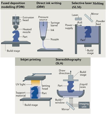
Figure 1. Popular additive manufacturing methods. Reprinted by permission from Macmillan Publishers Ltd: Nature Reviews Materials [30], Copyright (2018).
Download figure:
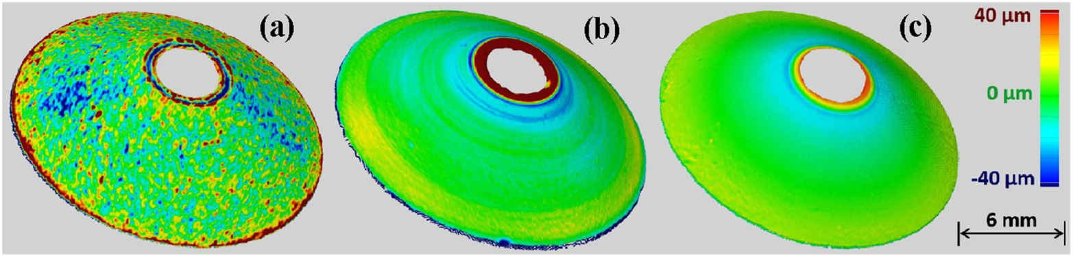
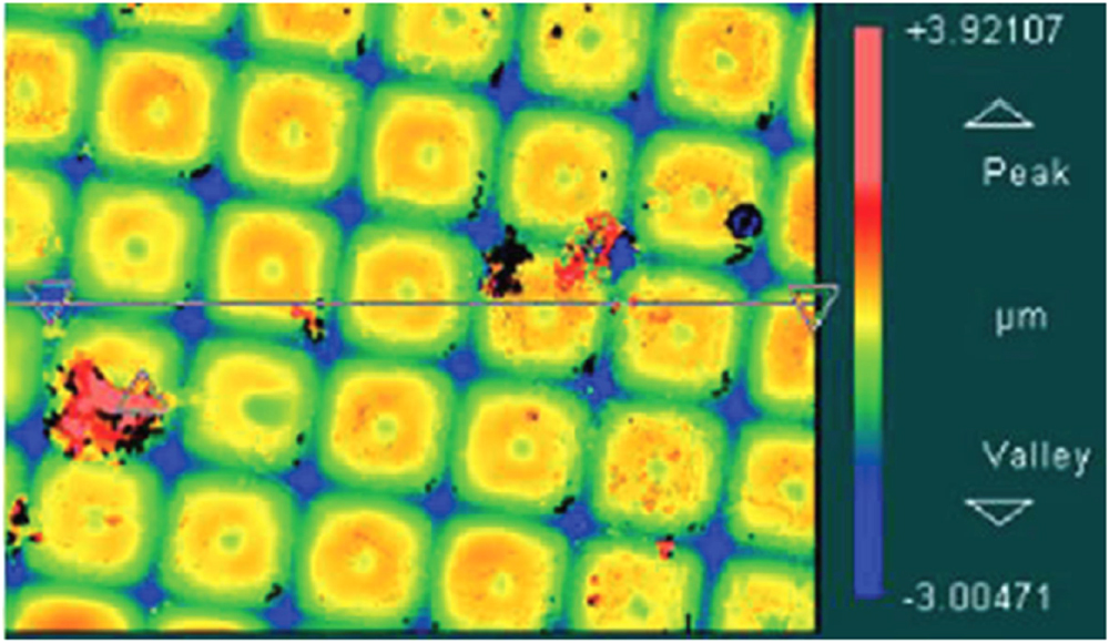
Standard image High-resolution imageSince roughness on the surface created with this technique is not normally suitable for optical components, post-processing, such as sand blasting, milling, and polishing, is required. For instance, a conic mirror printed by SLM (figure 2) shows that the roughness is too high before post-processing (more than 40 μm). According to the results, grinding and polishing improve surface roughness of the area and can make it more consistent on the optical surface. However, the regions near corners, specifically the inner corners, still have relatively higher roughness.

Figure 2. Additively manufactured conic mirror assessment. (a) SLM printed part (b) after grinding and (c) after polishing. Reprinted with permission from [29].
Download figure:
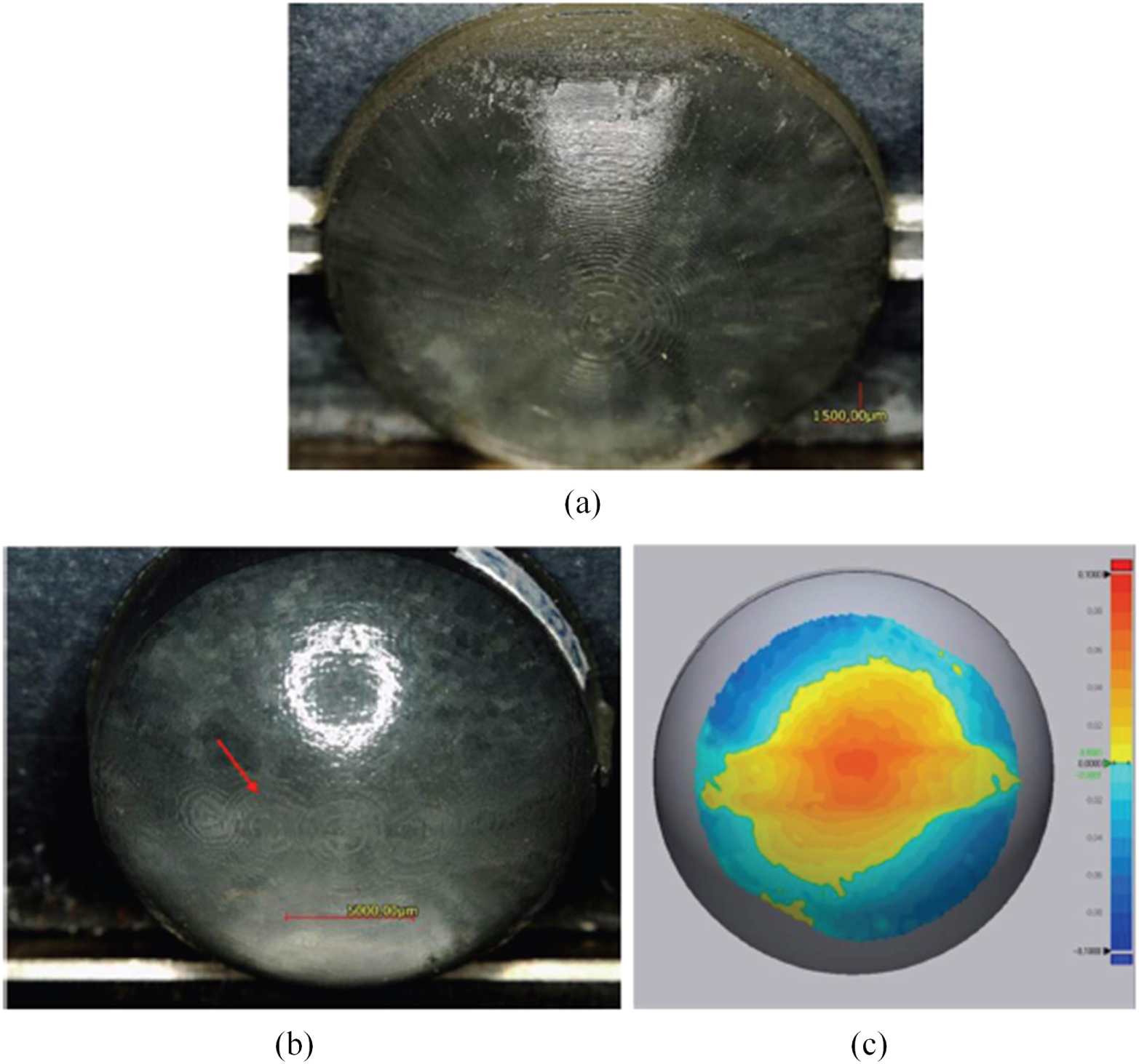
Standard image High-resolution imageIn other research [31], eight materials were chosen to investigate the capabilities of AM in fabricating mirrors and precision structures. The materials included aluminum (Al), titanium (Ti), beryllium (Be), aluminum beryllium (Al–Be), Inconel 625, stainless steel/bronze, and polyether-ether-ketone (PEEK) polymer. The study showed that printed surfaces with 6 nm roughness can be obtained after post-processing. In the end, after comparison to conventionally manufactured parts, the authors concluded that all of the mirrors fabricated showed excellent density, dimension, stability, and homogeneity of thermal expansion over temperature in the scale of optical measurement. Figure 3 shows the mirror fabricated by AM and its surface roughness. The results obtained showed that the center and outer regions of the mirror were less smooth, the same findings as a previous investigation [29].
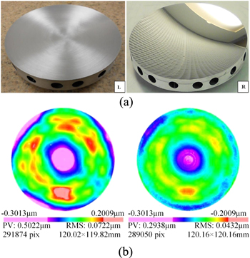
Figure 3. (a) A mirror manufactured by AM before post-processing (left) and after post-processing (right) and (b) surface roughness before (left) and after (right) the finishing process. Reprinted with permission from [31].
Download figure:
Standard image High-resolution image2.2. Fused deposition modeling
Melting one or more filament materials and depositing the melts onto a substrate, layer by layer, is the core concept of FDM. In this technique, the filament is passed through a hot nozzle; and the melt solidifies on the substrate or a previous layer, as shown in figure 1 [32]. Although this method is both simple and cost-effective, its quality does not meet the requirements for precision optical components. Components manufactured by this technique commonly suffer from inhomogeneity and low surface quality, both of which can result in strong light-scattering effects [33, 34]. To use these components as reflective optical elements, such as mirrors, post-processing procedures are required, such as machining [35], etching in chemical solution [36], and thermal processing [37]. Recently, Chen et al [38] evaluated reflectivity of surfaces parts fabricated by FDM after post-processing (re-forming with loading and heat applied).
In spite of the aforementioned limitations, FDM has been utilized to fabricate different optical fibers, such as air-structured optical fiber [39]. Figure 4 shows the printed part (before and after the annealing process) along with the light beam with different wavelengths transmitted by the printed optical fiber. Using the same process as for step-index optical fibers [40], microstructured polymer optical fibers [41, 42], optical fibers with special-shaped cores [43], have been developed.

Figure 4. The printed optical fiber (left) and transmitted light with different wavelengths (wavelength = 630 nm, 515 nm, white light, and experimental setup) (right). Reprinted with permission from [39], © 2015 Optical Society of America.
Download figure:
Standard image High-resolution imageRecently, Wang et al fabricated FDM-based 3D printing to manufacture air-clad coherent fiber optic faceplates [44]. Using the same method, a faceplate containing 200 00 fibers with a spatial resolution of up to 1.78 LP mm−1 was produced. Transmission and cross-talk of the faceplate, compared to commercial counterparts, showed that the method has the potential to be used instead of the conventional manufacturing process for fiber optical devices (figure 4). Transmission of the printed optical fibers as a function of the faceplate length and a comparison to its commercial counterpart are shown in figure 5.

Figure 5. Transmission of the printed optical fibers. Reprinted with permission from [44], © 2018 Optical Society of American.
Download figure:
Standard image High-resolution imageIn FDM-based optical fiber printing, temperature distribution in the nozzle is the main factor affecting the manufacturing process [45]. Also, annealing as a vital post-processing step plays an important role in the improvement of optical components. Figure 6 shows ultraviolet (UV)-visible and infrared (IR) spectra for the annealed and non-annealed fabricated fibers.

Figure 6. Transmission ranges of annealed and non-annealed fabricated fibers. (a) UV-visible spectra and (b) IR spectra. Reprinted with permission from [39], © 2015 Optical Society of America.
Download figure:
Standard image High-resolution image2.3. Stereolithography
This AM technique is based on solidifying curable polymer materials by UV light. As depicted in figure 1, a layer of polymer is solidified; and then a new layer of photoresist is placed on the formed layer. By repeating this process, the optic is manufactured layer by layer. Two main approaches to UV exposure are laser beam spot scanning and light pattern projections [46, 47]. Since each layer is fabricated by a single exposure in light pattern projection using a digital micromirror device (DMD), the printing speed is significantly enhanced compared to the single spot scanning method. Drawbacks of light-projection-based techniques are a higher power light source being required, the negative effect of the projection's pixel size on the print quality, and no control of the penetration of light energy [48]. Figure 7 shows white light interferometer scans of a DMD-SLA printed specimen. As seen in the figure, the surface of the sample had a pixelated structure [20]. Although the quality of the optical components made by SLA appears to be adequate, in most cases, improvements are still needed in both vertical and lateral resolution. A step profile of a spherical lens sample and shape deviation of a lens manufactured by SLA are shown in figure 8 [20]. According to the figure, shape deviation is higher in the center of the printed sample. Using SLA, Kukkonen et al fabricated nonlinear optical lenses (NOL). Based on the results obtained, they demonstrated that SLA has good potential as a highly efficient manufacturing method for NOL [49].

Figure 7. Pixel structure of the sample manufactured using DMD-SLA. Reprinted with permission from [20].
Download figure:
Standard image High-resolution image
Figure 8. (a) A lens manufactured by SLA, (b) step profile, and (c) shape deviation. Reprinted with permission from [20].
Download figure:
Standard image High-resolution image2.4. Multiphoton stereolithography
This technique is based on curing resins using an ultrafast laser. Once the laser, with a pulse duration in the range of tens or hundreds of femtoseconds, hits the photosensitive material, a multiphoton absorption phenomenon may happen in the very center of the focus beam region [50–52], roughly on the order of tens of nanometers. The main advantage of MPS over SLA is the possibility of achieving nanometer resolution [53]. Using continuous beam movement, the optical component is created via a spot-by-spot curation process. The excellent smoothness of the surface parts fabricated using this method and the high optical clarity are the reasons why this technique is a fascinating approach to fabricating precision optical components [53]. MPS is utilized to manufacture a wide range of precision optical components, such as microlens arrays (MLAs), waveguides, and photonic crystals [54–56].
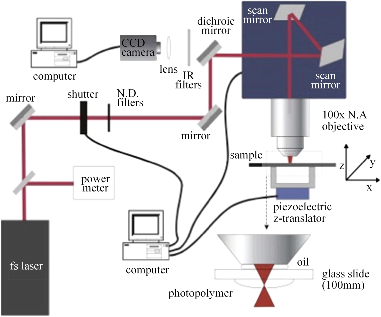
As an important optical component in photonic systems, microlenses (MLs) have made it possible to build high-performance, miniaturized systems for a wide range of applications, such as imaging, sensing, and optical communication [57–59]. AM has been used to fabricate MLs and MLAs. MPS using a femtosecond laser is a common method of fabricating MLAs. Using two-photon polymerization (TPP), Guo et al fabricated a 2 × 2 spherical microlens array (diameter: 15 μm) [54] and a Fresnel lens (diameter: 17 μm). Figures 9 and 10 show the microspherical and Fresnel lenses fabricated by MPS and their performance, respectively. Larger MLAs on the scale of hundreds of microns is reported by Chung et al [60]. In the same manner, cylinder and axicon MLs were fabricated by Li et al [61] with a resolution of up to 1.5 μm. Laser beam scanning is the common method used in MPS experiment setups [62]. In this technique, a combination of linear stages and galvano mirrors are normally used [62]. For instance, the experimental setup used by Malinauskas et al to fabricate arrays of custom-parameter spherical lenses is illustrated in figure 11 [63].

Figure 9. Images of the microlens fabricated in [54]. (a), (b) 2 × 2 microspherical lenses and a magnified view, micro-Fresnel lens manufactured using several lateral scanning steps (bottom figures). Reprinted with permission from [54], © 2006 Optical Society of America.
Download figure:
Standard image High-resolution image
Figure 10. (a), (c) Optical performance spherical microlenses and (b), (d) micro-Fresnel lenses fabricated by MPS. Reprinted with permission from [54], © 2006 Optical Society of America.
Download figure:
Standard image High-resolution image
Figure 11. (a) Experimental setup and (b) microlenses fabricated using MPS. Reproduced from [63]. © IOP Publishing Ltd. All rights reserved.
Download figure:
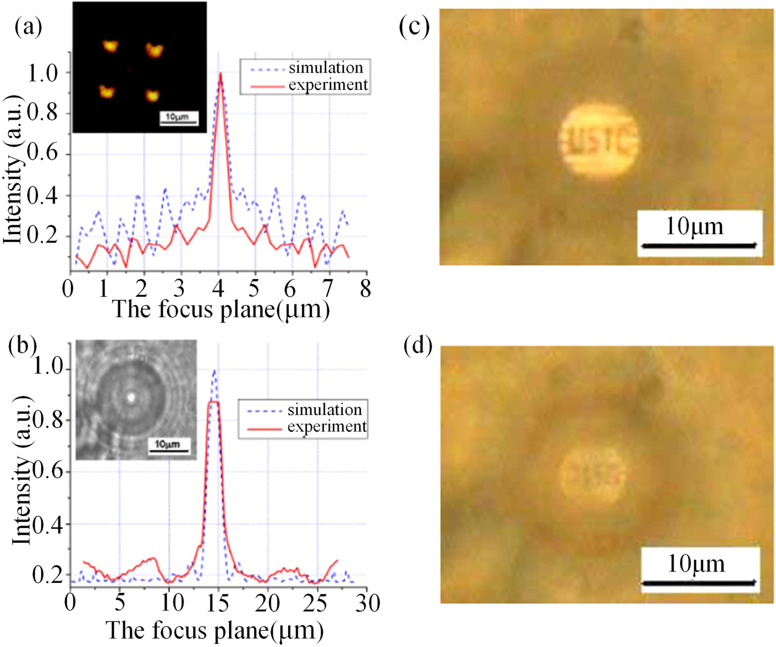
Standard image High-resolution imageSince MPS has a higher resolution compared to other AM fabrication methods, it has been used to manufacture mesoscale structures and large lenses. Mesoscale structures have an overall size of up to centimeters but with micro- or nanosize features [64]. To demonstrate MPS capabilities in the fabrication of mesoscale structures, a large butterfly (in the range of a millimeter) with micro- and nanoscale features is shown in figure 12 [64]. Mesoscale lenses have a wide range of applications, such as ophthalmology and imaging systems. In ophthalmology, according to a study on printing customized ocular and intraocular mesoscale lenses, the printed lenses do not meet clinical standards due to high surface roughness and low transparency in the visible light spectrum [65–67]. However, making an optical component of an eye has been attempted [68]. A comparison between the different printing techniques can be found in [21, 33, 69]. Figure 13 shows a mesoscale precision lens fabricated by AM and its optical performance in forming an almost perfect focus.

Figure 12. (a) Scanning electron microscope (SEM) image of the whole structure. (b) Enlarged view of the antennas. (c) Close-up view of the microlenses on the head, and (d) embedded nanolattice of a wing [64].
Download figure:
Standard image High-resolution image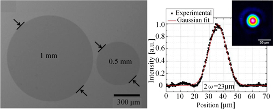
Figure 13. A lens on the scale of millimeters and its corresponding performance graph [64].
Download figure:
Standard image High-resolution imageAccuracy of optical components in a 3D printing process depends on the size of the voxels (minimum fabrication unit). Improving the accuracy requires a reduction in voxel size, which leads to a rise in production time and cost [70]. Partially for this reason, research in the development of systems or processes for manufacturing macroscale lenses by AM has been limited. Among 3D printing technologies, it has been demonstrated that multiple photon polymerization (MPP) has the highest resolution in comparison to other printing techniques (around 100 nm or less) [21, 69, 71]. Research in resolution improvement of mesoscale lenses fabricated by MPP is limited to process improvements by controlling parameters [72, 73] and developing new resins [74–76], new systems [16, 64, 77–79], or laser scanning algorithms [80, 81].
One of the main advantages of AM over conventional optical manufacturing is its capability of creating multicompound systems at different scales in a single setting without assembly. Recently, Thiele et al demonstrated 3D printing of multilens objectives directly onto a complementary metal-oxide semiconductor image sensor to produce a foveated imaging system (as in figure 14) [14]. Freeform optics printed on optical fibers is another application of MPS (figure 15) [82–84]. Multilens optical systems [70], combining both refractive and diffractive optics [84], are among the wide range of multicomponent that have been manufactured using MPS.
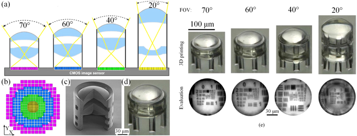
Figure 14. Three-dimensional-printed foveated imaging system. (a) Lenses with different focal lengths (f = 31, 38, 60, and 123 mm). (b) Pixelated image formed by the system. (c) Three-dimensional-printed doublet lens. (d) SEM image of the compound lens. (e) Printed lenses with different FOV (field of view) and corresponding imaging evaluation. Reprinted from [14]. © American Association for the Advancement of Science.
Download figure:
Standard image High-resolution image2.5. Direct inkjet writing
This technique is based on the ejection of small droplets of ink through a nozzle in a specified pattern. Then, the droplets solidify on a substrate to form the first layer [30]. The second layer is deposited in the same manner on top of the first layer. The component is built, layer by layer, in an iterative process. Figure 1 illustrates the principle of this process. The printable ink is pressured through the nozzles. The ink materials are designed such that they solidify once they are deposited on the substrate or the previous layer [85, 86]. This technique is also used to fabricate cavity microball lenses [87] and holograms generated on metal film [88].
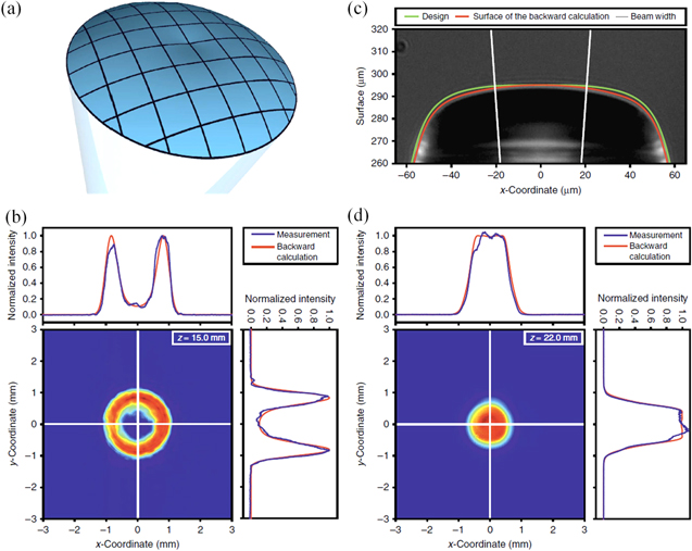
Figure 15. (a) Donut-shaped optical surface on an optical fiber. (b) Corresponding experimental result of a donut-shaped surface, (c) hat-shaped optical surface on the fiber, and (d) corresponding experimental result of hat-shaped surface. Reprinted by permission from Macmillan Publishers Ltd: Nature Communications [82], Copyright (2016).
Download figure:
Standard image High-resolution image2.6. Inkjet printing
Inkjet printing works by ejecting droplets from a nozzle (by pressure) and depositing them onto the substrate [89], as shown in figure 1. The major challenge is how to attach the droplets to each other to form continuous lines and surfaces [90]. In spite of this tough challenge, this technique has recently gained interest because of its good capability in controlling ejected droplets and depositing volume on the substrate [91]. Since the ink can be selected from a wide range of solvents, a large number of materials are possible for use in optical fabrication. This method has been used to fabricate optical components, such as optical waveguides, sensors, MLs, and detectors [92–98]. For instance, Xing et al [99] fabricated spherical and cylindrical MLs using this method (figure 16). Performance when printing large lenses using this technique has been evaluated in terms of surface roughness and imaging quality, as in [100]. Figure 17 shows a resolution test of a conventional and a printed lens [100]. The results obtained show that this technique is capable of manufacturing large lenses with a surface roughness in the range of injection-molded lenses.

Figure 16. Microlens fabricated by DIW. Reprinted with permission from [99], © 2016 Optical Society of America.
Download figure:
Standard image High-resolution image
Figure 17. Resolution test of (a) a conventional lens and (b) a printed lens. Reprinted with permission from [100].
Download figure:
Standard image High-resolution image3. AM of optics with features at nanoscale
AM has already been used for microscale rapid fabrication, and some methods have already been commercialized. However, AM methods at nanoscale are not widely adopted as yet, especially in commercial products. Photolithography is the primary conventional process for fabricating microstructures. However, at nanoscale, the diffraction limit of light restricts the application of UV photolithography [101]. Electron beam lithography can be used for nanofabrication; however, this method is expensive with an extremely low production rate. In addition, arbitrary 3D shapes cannot be made using the electron beam process without a major effort. As a possible alternative, AM can effectively reduce the cost and improve the fabrication efficiency and complexity [102]. These unique features of AM have been the focus of some recent research and development activities.
Different from microscale AM, additive nanomanufacturing (ANM) relies on some unique methods. There are two groups of ANM methods: DW and single particle placement. Usually, single particle placement methods are applied in the fabrication of atom-sized features. In the optical range, DW methods are more widely used. This section primarily discusses the two DW methods and their applications in manufacturing optical devices with nanoscale structures.
3.1. Dip pen nanolithography
DPN is a scanning probe microscopy-based nanofabrication process. This method can reach a resolution of sub-50 nm and can be adapted in large areas. Figure 18 shows DPN processes for manufacturing different optical devices or structures. During a DPN process, an inked tip is used to transfer materials through a meniscus that naturally forms between the tip and the substrate [102]. There are two types of inks. The first kind is a molecular ink, which is suitable for dry inks, while the second one is liquid [103]. Features are formed by either chemisorption or self-assembly physisorption [101, 102]. Since this process does not require UV or electron beam exposure, DPN is adaptable for both inorganic and organic materials. In addition, as shown in figures 18(a) and (b), the DPN process can be combined with more conventional fabrication methods, such as photolithography and wet etching.
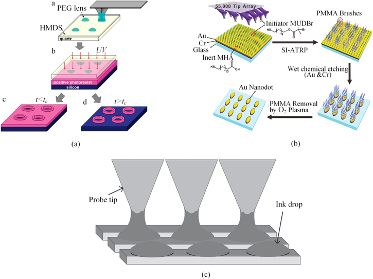
Figure 18. Schematic diagrams for some DPN processes. (a) DPN fabrication for polyethyleneglycol (PEG) lens arrays on top of the hexamethyldisilizane (HDMS)-coated quartz glass; subsequently, this array was used for ultraviolet photolithography. Reprinted with permission from [101]. Copyright (2010) American Chemical Society. (b) The DPN method was used to fabricate polymethylmethacrylate (PMMA) brushes on a gold surface to prepare for wet etching. [104] John Wiley & Sons. © 2017 WILEY-VCH Verlag GmbH & Co. KGaA, Weinheim. (c) DPN is used as liquid ink to create dot patterns. [103] John Wiley & Sons. © 2018 WILEY-VCH Verlag GmbH & Co. KGaA, Weinheim.
Download figure:
Standard image High-resolution imageAs mentioned above, the DPN method is suitable for fabrication of nanoscale structure patterns. This means that optical structures with nanoscale patterns, such as periodic gratings with small grating constants and nanoscale lens arrays, can be manufactured by the DPN method. Figure 19 shows DPN fabrication results and the optical properties. In figure 19(a), Jang et al [101] fabricated a PEG lens array using DPN. This lens array was then used for subsequent UV photolithography. Chen et al [104] manufactured a series of PMMA brushes above a gold surface with a large area (as shown in figure 19(b)). With the help of PMMA brushes, the wet etching process was applied; and gold nanostructures for optical applications were fabricated on a large-area glass substrate. This gold nanoscale pattern substrate can be used for a replica of antireflective coating on the surface of solar cells (figure 19(d)). Zohar et al [103] tried to use DPN to fabricate polydimethylsiloxane (PDMS) nanoscale gratings (in figure 19(c)) to show the potential for using the DPN method in the manufacturing of nanoscale optical gratings. The results of an experiment for such a PDMS grating are shown in figure 19(e).

Figure 19. Fabrication results of DPN. (a) Atomic force microscopic (AFM) image of the PEG nanoscale lens arrays generated by DPN. The different size of each row is attributed to different substrate dwell times. Reprinted with permission from [101]. Copyright (2010) American Chemical Society. (b) AFM image of PMMA brushes preparing for wet etching fabrication by DPN. [104] John Wiley & Sons. © 2017 WILEY-VCH Verlag GmbH & Co. KGaA, Weinheim. (c) AFM image of the grating pattern array; different lines are fabricated by different tip velocities. John Wiley & Sons. © 2017 WILEY-VCH Verlag GmbH & Co. KGaA, Weinheim. (d) Transmission rate of the incident light with different wavelengths on the substrate with or without gold nanoscale patterns. [104] John Wiley & Sons. © 2017 WILEY-VCH Verlag GmbH & Co. KGaA, Weinheim. (e) Experimental device used to measure diffraction orders and the diffractive spectrum of the grating fabricated by DPN. [103] John Wiley & Sons. © 2017 WILEY-VCH Verlag GmbH & Co. KGaA, Weinheim.
Download figure:
Standard image High-resolution image3.2. EHD jet printing
EHD jet printing is similar to inkjet printing, which is widely used in printers in the office and at home. EHD jet printing can be used for the fabrication of nanostructures. The highest resolution of the EHD jet printing method can reach 10 nm. Figure 20 is a diagram of EHD jet printing. The EHD method uses an electric potential applied between the nozzle and the substrate. With the help of the electric potential, mobile ions accumulate near the nozzle and form into a Taylor cone. In low electric fields, the Taylor cone will produce droplets periodically (as shown in figure 20). Figure 21 shows several types of EHD jet printers. If the applied voltage is very high, multiple jets can be produced and a continuous flow generated. In this case, EHD jet printing has already become EHD spraying, which is widely used in the fabrication of thin film deposition [105, 108]. Engstrom et al [102] and Wang et al [105] summarized the application of EHD jet printing in general ANM cases.
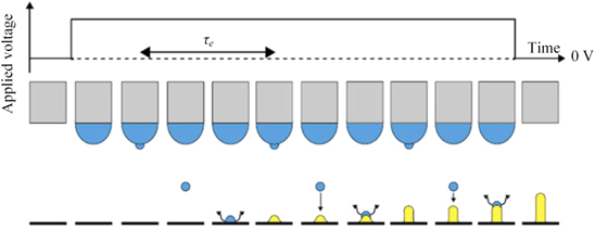
Figure 20. Schematic diagram of EHD jet printing. Reprinted with permission [102].
Download figure:
Standard image High-resolution image
Figure 21. Schematic diagram of four different types of EHD jet printers. Reproduced from [106] with permission of The Royal Society of Chemistry.
Download figure:
Standard image High-resolution imageIn optical applications, scientists have already adapted the EHD jet printing method to fabrication of micro- or nanoscale optical structures. Sutanto et al [107] used the EHD jet printing method to fabricate three different microoptics devices to demonstrate the potential for using EHD jet printing in the manufacturing of optical nanostructures (as shown in figures 22(b)–(d)). Both Vespini et al [106] and Coppola et al [108] used the forward pyro-EHD jet printing process (as shown in figure 22). This type of EHD jet printing process uses the pyroelectricity effect to provide the electric field needed in EHD jet printing. As a result, they compared the forward EHD jet printing process by using different materials (PMMA, PDMS, polylactic-co-glycolic acid (PLGA), and nanometal inks) and chose PDMS as the raw material to fabricate a microlens array [108]. The fabrication results are shown in figure 22(a).

Figure 22. Some fabrication results of EHD jet printing. (a) PDMS microlens array fabricated by forward EHD jet printing. Reprinted with permission from [108]. (b) Optical microscope image and AFM image of microlens array. (c) Optical microscope image of EHD printed waveguides and illustration of a waveguide. (d) Image of EHD jet printed grating and the diffraction when a collimated laser beam passes through the grating. (b)–(d) Reprinted from [107], Copyright (2014), with permission from Elsevier.
Download figure:
Standard image High-resolution image3.3. DLW and metamaterial
In nanoscale additive fabrication, DLW is also considered to be one of the mainstream methods. Although DLW is a photoresist-based method, nothing additional is needed after the shape is created by DLW, which is similar to additive fabrication [102]. As mentioned before, some DLW methods, such as SLM and MPS, are widely used in mesoscale additive fabrication. Today, the TPP method of MPS is one of the successful methods that has been utilized in nanoscale additive fabrication [102]. Selimis et al [109] wrote a review on the general approach of DLW as a 3D printing method from principle to application (figure 23). In optical applications, Chen et al [110] used DLW to fabricate one-dimensional (1D) antireflective rectangular gratings on the surface of gallium arsenide (GaAs) solar cells and used finite difference time domain (FDTD) to simulate the grating property. Li et al [111] utilized 3D TPP to fabricate near-infrared antireflective coatings. Moisset et al [112] used DLW to manufacture nonlinear optical thin film with a thickness down to 20 nm. Al-Qattan et al [113] demonstrated fabrication results of 1D and two dimensional nanophotonic structures whose scale was around 900 nm on contact lenses.

Figure 23. Schematic diagram of a typical DLW experiment system. Reprinted from [109], Copyright (2015), with permission from Elsevier.
Download figure:
Standard image High-resolution imageAnother significant application of DLW is in the fabrication of optical metamaterials. The unique optical properties of metamaterials do not exist in natural materials. The realization of these unprecedented properties requires nanostructure arrays in different dimensions. Boltasseva et al [114] reviewed several common fabrication methods in the manufacturing of optical metamaterials with negative refractive indices. Among these methods, the DLW method, specifically TPP, was considered to be the most promising method for fabrication of large-area 3D metamaterials [114]. Recently, an increasing number of studies applied the DLW method to fabrication of different metamaterial structures. Figure 24 shows some examples. Moughames et al [115] reported a fabrication of metamaterial IR concentrator using 3D laser writing (as shown in figure 24(a)). They used the FDTD method to simulate the electronic field distribution and experimentally measured the optical performance by using an IR charge-coupled device. Faniayeu et al [116] designed a perfect electromagnetic wave absorber based on 3D vertical split-ring resonators (as shown in figure 24(b)). They used the DLW method to create the required submicron resolution for the structure. Li et al [117] utilized the 3D DLW method to fabricate 1D high-contrast, infrared polymer photonic crystals. As shown in figure 24(c), they designed a 1D structure array in each layer and packed multiple layers vertically. An SEM image of the fabricated structure stack after 3D DLW is shown in figure 24(d).

Figure 24. An example of DLW used in the fabrication of optical metamaterials. (a) SEM images of the metamaterial concentrator for a wavelength of 10.4 μm (left) and 5.6 μm (right). Reprinted by permission from Macmillan Publishers Ltd: Scientific Reports [115], Copyright (2016). (b) SEM image of vertical split-ring resonators. The top image is a closely packed case, and the bottom image is a merged case. Reproduced from [116]. © IOP Publishing Ltd. All rights reserved. (c) Numerical design of the 1D PCs. (d) SEM image of the 1D PCs fabricated. (c), (d) Reprinted with permission from [117], © 2018 Optical Society of America.
Download figure:
Standard image High-resolution image
4. Conclusions
This review summarized recent developments in the AM of precision optical devices. These processes have shown promising results in the manufacturing of high performance optical components. The devices and systems consisting of these components have also demonstrated unique features and performance. The exact capability of this exciting technology is difficult to determine based on the existing information. Nevertheless, this review clearly described a promising group of processes with mounting evidence that AM could potentially revolutionize optical fabrication in the near future.
Based on the current research and development in 3D AM for optical fabrication, much remains to be done in the near future, particularly in the manufacturing of regular size optical elements, e.g. optics in the size of a few inches. Even at micro- and nanoscale levels, the most promising results appear to only have occurred in lab settings rather than production environments. There are many unanswered questions and issues before this technology can be widely adopted. These issues include, but are not limited to, things such as index distribution, geometry, and volume shrinkage of the optical elements.
The aim of this review is to serve as a platform for researchers and industrial communities to engage and eventually implement this cutting edge manufacturing process and its associated products.