

Abstract
The extremely high peak intensity associated with ultrashort pulse width of femtosecond (fs) lasers enabled inducing nonlinear multiphoton absorption in materials that are transparent to the laser wavelength. More importantly, focusing the fs laser beam inside the transparent materials confined the nonlinear interaction to within the focal volume only, realizing three-dimensional (3D) micro/nanofabrication. This 3D capability offers three different processing schemes for use in fabrication: undeformative, subtractive, and additive. Furthermore, a hybrid approach of different schemes can create much more complex 3D structures and thereby promises to enhance the functionality of the structures created. Thus, hybrid fs laser 3D microprocessing opens a new door for material processing. This paper comprehensively reviews different types of hybrid fs laser 3D micro/nanoprocessing for diverse applications including fabrication of functional micro/nanodevices.
Export citation and abstract BibTeX RIS

Original content from this work may be used under the terms of the Creative Commons Attribution 3.0 licence. Any further distribution of this work must maintain attribution to the author(s) and the title of the work, journal citation and DOI.
1. Introduction
Three-dimensional (3D) printing has revolutionized manufacturing since it can create true 3D structures that are impossible to create using existing manufacturing techniques [1]. 3D printing, in principle, relies on additive manufacturing, by which not any kinds of structure can be created. Therefore, a successive procedure of additive and subtractive manufacturing, i.e. hybrid additive and subtractive manufacturing, to enrich the created structures has recently been attracting much attention [2].
Lasers are one of the most powerful tools for 3D printing. Among the lasers, femtosecond (fs) lasers, which emit ultrashort pulses with widths from several tens of fs to several hundred fs, can offer other 3D manufacturing schemes in addition to additive manufacturing [3]. Specifically, the extremely high peak intensity associated with the ultrashort pulse width of fs lasers can induce nonlinear multiphoton absorption in materials that are transparent to the wavelength of incident laser beam. Then, by focusing the fs laser beam inside the transparent materials, the nonlinear interaction can be confined within the focal volume only. By scanning the focused laser beam inside the transparent material, the material can be processed in a 3D manner along the trajectory of the focused laser beam, enabling 3D manufacturing. Another feature of fs laser 3D processing is the capability of nanofabrication far beyond the diffraction limit based on nonlinear absorption combined with suppression of the thermal effect [4, 5].
The 3D capability of a fs laser involves undeformative, subtractive, and additive processing (figure 1). Specifically, the undeformative processing performs internal refractive index modification to fabricate 3D optical microcomponents, such as optical waveguides, beam splitters and couplers, Bragg gratings, Mach–Zehnder interferometers, etc, inside transparent materials, such as glass and polymers [6–9]. Subtractive processing can realize the direct fabrication of 3D microfluidics, micromechanics, and photonic microcomponents in glass by fs laser 3D direct writing followed by chemical wet etching (fs-laser-assisted etching (FLAE)) [10–13]. Additive processing represented by two-photon polymerization (TPP) enables the fabrication of 3D micro/nanostructures made of not only polymer but also protein for photonic, microfluidic, and biological applications [4, 14–17].

Figure 1. Three different schemes in 3D processing achieved by fs laser: (a) undeformative, (b) subtractive, and (c) additive.
Download figure:
Standard image High-resolution imageFurthermore, a hybrid approach of different schemes enables creating much more complicated 3D structures and thereby promises to enhance functionality of the structures created. For example, a successive procedure of FLAE and undeformative optical waveguide writing realizes optofluidics for detection, manipulation, and sorting of bio samples [18–21]. Meanwhile, a combination of subtractive FLAE and additive TPP is a tool that can not only tailor 3D structures but also construct a biomimetic in vivo environment inside glass microfluidic chips [21–25]. Specifically, the subtractive FLAE can flexibly fabricate 3D microfluidic structures embedded in glass microchips without a complicated procedure of stacking and bonding of glass substrates. Subsequent TPP can then integrate complex shapes of 3D polymer structures with a nanometric feature size, because of its high fabrication resolution, to create biomimetic structures inside the glass microfluidic structures. These advanced biochips can be utilized to study the mechanisms of cancer cell invasion and metastasis [24] and many other areas of biological research.
This review paper first discusses the principle of 3D fabrication by fs laser and then introduces each fs laser scheme for 3D processing: undeformative, subtractive, and additive. Finally, different types of hybrid fs laser 3D microprocessing and their applications, including fabrication of functional micro/nanodevices, are comprehensively reviewed, followed by a final summary.
2. Principle of 3D fabrication by fs laser
When light is incident on a material, photons in the light are first absorbed by electrons. Metals can absorb any kind of laser beam due to a lot of free electrons, not taking reflection into account. For semiconductors and insulators, which have few free electrons, strong light absorption occurs to excite electrons from the valence band to the conduction band when the light with a photon energy, hν, larger than the bandgap, Eg, of the material is incident. In this case, a single photon can excite a single electron, so that the absorption process is called single-photon absorption. Single-photon absorption is a linear absorption process proportional to the laser intensity.
Light, whose photon energy is smaller than the band gap, is transmitted by the material as there is no possibility of electron excitation (figure 2(a)). However, if a large amount of photons are spatiotemporally incident on the material whose bandgap is larger than the photon energy, multiple photons can collaborate to excite a single electron to induce absorption [26]. This absorption process is called multiphoton absorption and n-photon absorption when n photons are required to excite a single electron (figure 2(b)). Multiphoton absorption is a nonlinear absorption process, and the absorption cross-section for n-photon absorption is proportional to the nth power of laser intensity. Such high-density photons in both space and time domains can be easily obtained by fs laser due to extremely high peak intensity, easily exceeding 1015 PW cm−2. Thus, the fs laser can perform high-quality microfabrication of transparent materials, such as glass, based on the multiphoton absorption [27, 28].

Figure 2. Electron excitation process in bandgap materials by (a) single and (b) multiphoton absorption.
Download figure:
Standard image High-resolution imageWhen the fs laser beam is focused inside the transparent material at an adequate pulse energy, the multiphoton absorption can be efficiently confined only at the focal volume. Then, by scanning the focused laser beam inside the transparent material in arbitrary directions, the material can be processed in a 3D manner, as shown in figure 3.

Figure 3. Schematic image of internal modification and 3D processing in a transparent material based on multiphoton absorption using fs laser.
Download figure:
Standard image High-resolution imageAnother important feature of fs lasers is the capability of achieving a super high resolution beyond the diffraction limit of the laser beam. Typically, the fs laser beam has a Gaussian beam profile in a space, and the spot size, ω0, focused by a lens with a numerical aperture (NA) is given by

where λ is the wavelength of the laser beam. Lenses with an NA larger than 1.0 are commercially available, for which a liquid immersion scheme is employed. Thus, the achievable spot size can be almost the same as the wavelength or even a bit smaller. The multiphoton absorption can restrict the absorption to an area smaller than the spot size to improve the fabrication resolution by adjusting the pulse energy, since the absorption cross-section for n-photon absorption is proportional to nth power of laser intensity [3]. Specifically, defining the effective spot size for the multiphoton absorption, ω, as the diameter where the multiphoton absorption efficiently takes place in the focal volume, ω, is given by

It is obvious that the effective beam spot size can be narrower than the actual spot size to overcome the diffraction limit. The higher the order of the multiphoton absorption, the smaller the effective spot size (figure 4).

Figure 4. Actual beam profile (thick dashed line) and spatial distributions of laser energy absorbed by transparent materials by two- (solid line) and three-photon (thin dashed line) absorption. The solid and straight line correspond to the threshold intensity to the reaction.
Download figure:
Standard image High-resolution imageThe Gaussian beam profile of a fs laser can further improve the fabrication resolution by a combination of the threshold effect and the multiphoton absorption [4]. For example, by adjusting the laser energy to induce the reaction at the laser intensity only above the solid horizontal line in figure 4, the fabrication resolution can be reduced to 2/5 of the actual spot size. Theoretically, the fabrication resolution can be improved with no limitation when taking advantage of the threshold effect if the laser intensity can be set to exceed the threshold intensity only at the most center part of the focused beam. However, in practice, the fabrication process becomes extremely unstable due to the difficulty of precisely and stably controlling the laser output energy as the laser intensity is near the threshold intensity. Thus, the fabrication resolution for a conventional scheme using a high NA objective lens is typically ∼100 nm, at the smallest.
3. Different schemes in 3D fabrication by fs laser
3.1. Undeformative processing
Multiphoton absorption induced by fs laser can bring about diverse microscopic structural changes without visible deformation inside the transparent materials in a spatially selective manner. The most famous phenomenon generated by the structural change is permanent refractive index changes [6], which can be performed in a variety of transparent materials, including glass, crystals, and polymers. The changes in the refractive index are considered to be a synergetic effect of the interaction of different phenomena, including formation of color center, densification and stress generation, redistribution of elements, heat diffusion, and accumulation. However, the true factors have not yet been quantitatively understood and may differ depending on types of materials [29]. The refractive index change was applied to write 3D optical waveguide by creating continuous lines with an increased refractive index. The refractive index can be typically increased by 10−3 ∼ 10−2. The waveguide writing is typically carried out using a transverse writing scheme, in which the sample (or the laser beam) is translated perpendicular to the direction of laser beam propagation. This specific capability allows us to write optical waveguides with arbitrary lengths and 3D geometries (figure 1(a)).
Refractive index modification can be utilized to construct 3D photonic microdevices including optical couplers and splitters [8], volume Bragg gratings [30], diffractive lenses [31], and compact and efficient single-longitudinal-mode lasers [32].
3.2. Subtractive processing
The microscopic structural changes generated by multiphoton absorption can also modify chemical properties inside the transparent materials. The chemically modified regions can be selectively etched away by successive wet etching, typically in a diluted hydrofluoric (HF) acid solution [11]. Femtosecond-laser-induced internal modification followed by chemical wet etching can create 3D microfluidic structures inside specific glass, specifically photosensitive glass [10, 12, 13] and fused silica [33] (figure 1(b)). This 3D glass micromachining technique has been referred to as FLAE or fs laser irradiation followed by chemical etching (FLICE). For the photosensitive glass, thermal treatment is necessary after the fs laser direct writing to develop the modified regions at the laser-exposed regions [34]. Unlike photosensitive glass, an enhanced etch rate in HF acid can be realized directly in fused silica by fs laser irradiation without employing subsequent thermal treatment [11]. Fused silica has some advantages over the photosensitive glass due to a wider range of transmittance from ultraviolet (UV) to infrared (IR) as well as fewer process steps, while a much smoother surface for the photosensitive glass of the microfluidic structure can be obtained by post-thermal treatment after chemical etching [35]. For both glasses, the narrowest microchannel width achievable is several μm due to a limited etching selectivity of typically ∼50 between the modified and unmodified regions. Femtosecond-laser-assisted etching can fabricate not only 3D microfluidic structures but also microoptical components, such as micromirrors [35] and microlenses [36, 37], and micromechanical components, such as microvalves [38] and micropumps [39].
3D microfluidic structures can also be formed inside glass substrates by fs laser 3D direct write ablation in liquid (typically water), a process frequently called liquid-assisted fs laser drilling (LAFLD) [40]. The liquid introduced into the fabricated microchannel can help to efficiently remove ablation debris, so that the drilling length can be greatly enhanced as compared with that achieved by drilling in ambient air. Since this technique does not rely on generating etch selectivity in materials by fs laser irradiation, it can be applied to any material that is transparent to the writing pulses [41]. Furthermore, LAFLD can be used to fabricate nanochannels since this process relies on ablation. In fact, nanochannels with diameters of ∼700 nm and arbitrary geometries have been fabricated using a high NA objective lens [42].
3.3. Additive processing
Laser stereolithography is one conventional 3D printing technique that can be used to create 3D structures [43]. In this process, a thin layer of photocurable epoxy resin is first formed on a substrate equipped on an elevator stage in a vat. A focused UV light beam (typically a helium cadmium (HeCd) laser) is then scanned (or the light is projected through a photomask) in the plane of the thin layer. The epoxy resin is initially liquid, but it solidifies along the light beam trace by photopolymerization. After the light exposure, the elevator stage is shifted down in the vat to form the second thin epoxy resin layer on the created structure, and the focused light beam is again scanned in the plane of the second layer. Repeating this layer-by-layer process thus enables fabrication of 3D structures.
The use of a near-IR or visible fs laser for stereolithography instead of a UV light beam, which is transparent to the photocurable epoxy resin, allows us to directly create 3D structures without shifting the elevator stage, by internal modification due to two-photon absorption (figure 1(c)) [4]. Stereolithography with a fs laser is termed TPP. TPP transforms small unsaturated molecules in a liquid state to macromolecules in a solid state due to polymerization reactions. Only the regions in epoxy resin where a laser beam is focused at an adequate pulse energy are solidified since the two-photon absorption can be confined in the focal volume. The unpolymerized resin is easily washed away with a solvent by the subsequent developing process to leave the created 3D structure unchanged. A solid resist can be also used for the direct fabrication of 3D micro/nanostructures instead of epoxy resin. Use of the solid resist makes it much easier to create complicated 3D microstructures and topologically complex shapes. Different from epoxy resin, the solid resist can be employed to implement subtractive fabrication as well as additive fabrication by the selection of a suitable photoresist (positive or negative resist).
As described in section 2, synergetic contribution of the multiphoton absorption and the threshold effect typically achieves ∼100 nm fabrication resolution in TPP when using the objective lens with an NA of 1.4, even for a laser wavelength of ca. 800 nm [44]. Precise setting of the laser intensity to very near the TPP threshold intensity coupled with control of the laser scanning speed enables reduction of the fabrication resolution down to 18 nm [45]. However, reproducibility with such an extremely high resolution is very poor due to the inherent sensitivity of the fabrication process to fluctuations of the fs laser output power. The concept of stimulated emission depletion (STED) microscopy, which was originally developed for far-field bioimaging with a nanometer resolution [46], was adopted to achieve the super high resolution for TPP. In STED lithography, an inhibitor is mixed in the photoresist. Then, a circular shape of the excitation beam with, e.g. a wavelength of 800 nm and a pulse width of 200 fs, and a doughnut shape of the deactivation beam operated at the same wavelength but in continuous wave mode are superimposed to be coaxially focused in the negative-tone photoresist [47]. The excitation beam induces photopolymerization in the negative-tone photoresist, while the doughnut-shaped deactivation beam excites the inhibitor molecules, which inhibits photopolymerization triggered by the activation beam at the doughnut ring. As a result, the polymerization can be confined only at the center part of the excitation beam to achieve the fabrication resolution as small as 9 nm [48]. However, it is still very difficult to regularly produce 3D nanostructures with such a super high resolution.
TPP is currently widely utilized to create 3D polymer micro/nanostructures including photonic devices [49, 50], micro/nanomachines [51], microfluidic devices [52], medical and tissue engineering devices [16], etc. TPP can be extended to create 3D micro/nanostructures made of metals [53] and proteins [17] by multiphoton reduction and multiphoton crosslinking, respectively.
4. Hybrid fs laser 3D processing
As described above, fs laser direct writing offers three different processing schemes in 3D fabrication: undeformative, subtractive, and additive. Each process has its own advantages and drawbacks. For example, additive processing using TPP with a negative-tone resist is not suitable for the construction of large volume objects due to the bottom-up fabrication. In contrast, it is difficult to fabricate 3D fine structures with complex shapes by subtractive fabrication with FLAE or LAFLD. Thus, a combination of these fabrication processes could provide the possibility to diversify the geometry and/or enhance the functionalities of the fabricated structures.
4.1. Subtractive and undeformative processing
A combination of subtractive FLAE and undeformative refractive index modification of glass realizes fabrication of functional optofluidic systems. In this scheme, a 3D microfluidic structure is first fabricated inside glass by FLAE; and then the optical waveguides are integrated with the 3D microfluidic structure by the refractive index modification. The intrinsic properties of glass in the unexposed region do not significantly change after FLAE; optical waveguides can be successively written inside the glass.
One good example of an application of this hybrid technique is the fabrication of optofluidics for cell sorting using optical forces combined with fluorescence detection of the cells, as conducted by Bragheri and shown in figure 5(a) [54]. Two inlet channels (INs) were merged into a single straight channel where fluorescence detection and sorting were carried out, and the merged channel was then split into outlet channels (OUTs) to sort the cells. For fluorescence detection and sorting, optical waveguides guiding a probe beam for fluorescence detection (FWG) and an optical force beam for sorting (SWG) were integrated with the merged channel. Then, the sample liquid containing cells was injected from IN1, while a buffer solution was injected from IN2. By properly controlling the flow rates of each liquid, laminar flow was generated in the merged channel.

Figure 5. (a) Principle for cell sorting that utilizes optical forces combined with fluorescence detection. Demonstration of cell sorting when (b) nonfluorescent and (c) fluorescent cells are detected in the optofluidic device Reproduced from [54] with permission of The Royal Society of Chemistry.
Download figure:
Standard image High-resolution imageIn this scheme, the entire sample liquid with all of the cells flowed to OUT1. Introducing the sorting laser beam using SWG induced optical forces to push cells into the buffer solution side, so that the pushed cells were sorted in OUT2. Sorting can be automatically conducted by the fluorescence detection of cells with illumination of the fluorescence laser beam guided by FWG. By detecting the specific fluorescence signal from the target cell, the optical force laser beam was automatically switched on after a moderate delay time to irradiate the detected cells when they arrived in front of the SWG. The target cells were then pushed into the buffer solution side and eventually sorted to OUT2. Approximately 50% of the cells in the samples were stained with green fluorescent protein. For nonfluorescent cells, the sorting laser was kept switched off, since they did not emit a fluorescence signal by illumination of the fluorescence laser guided by the FWG. Then the cells were kept flowing into the sample solution and flowing to OUT1 (figure 5(b)). In contrast, when fluorescent cells were illuminated, fluorescence signals were detected. After a proper delay time, the optical force laser was switched on to push the cells into the buffer solution side. As a result, the targets cells were sorted to OUT2, as shown in figure 5(c).
Fabrication of optofluidic devices by subtractive FLAE and undeformative refractive index modification has been extensively demonstrated, with applications that have included concentration measurements of liquid samples [55], absorption and fluorescence spectra measurements of liquid samples [56], detection and manipulation of single cells [54, 57–59], and rapid screening of algae populations [21, 60, 61].
Another scheme of subtractive and undeformative processing is the integration of optical filters into 3D microfluidic devices. For FLAE of photosensitive glass, thermal treatment is employed after the fs laser direct writing to develop the modified regions at the laser-exposed regions. A crystalline phase of lithium alminometasilocate is grown using the thermal treatment [34]. The growth of crystalline phase transforms the colorless and transparent glass to a dark brown color. This color change can thus be utilized for the formation of optical filters. One layer of an optical filter can be formed by scanning the focused laser beam in the glass line by line in the same plane. One layer of the optical filter can cut approx. 29% of white light in the wavelength range from 400–700 nm. By stacking the filter layers at a pitch of 30 μm within the glass, the average transmittance can be stepwise adjusted from about 90% for no filter layer (about 10% is lost to surface reflection) to about 3% with ten filter layers.
In a study by Hanada et al, optofluidics integrated with optical filters were applied to investigate the effect of light illumination on Phormidium's gliding motion [55]. Phormidium are soil-dwelling unicellular and colonial cyanobacteria that form motile filaments. These filaments migrate in soil from the main biomass to nearby seedling roots where they form new colonies. Phormidium is ectosymbiotic, and the growth of the seedling accelerates after forming the association with Phormidium. Therefore, understanding the factors that induce Phormidium gliding is very important for developing a means to accelerate the growth of vegetable seedlings. Optofluidics integrated with optical waveguides fabricated by FLAE and the refractive index modification identified that carbon dioxide (CO2) secreted from the seedling root was the most likely attractant for the Phormidium gliding [55]. It was further revealed that light illumination was necessary for the gliding. To determine the light intensity necessary for the gliding, a 3D L-shaped microfluidic channel was fabricated in the photosensitive glass, part of which was covered with the optical filters (figure 6(a)). The same number of layers was formed above and below the channel. The microscope's light always illuminated the microfluidic channel from the bottom, and observations made using the microscope were obtained in a dark room so that the fabricated filters were able to control the light intensity in the microfluidic channel. Phormidium glided to the root in the microfluidic channels when five or fewer optical filter layers were integrated, while the Phormidium remained at the entrance of the channel even after 2 h when six or more optical filter layers were integrated (figure 5(b)). These results indicate that there is a threshold of white light intensity necessary for Phormidium to glide to a seedling root. The intensity of the microscope's white light was always kept at 17 000 lx. Thus, the threshold white light intensity for the Phormidium gliding must be slightly greater than 1530 lx, based on 9% average transmission in the wavelength range from 400 to 700 nm when six layers of optical filters are in place. This intensity corresponds to the illuminance at a depth of a few mm below the soil surface, where many bacteria, including Phormidium, live.

Figure 6. Integrated optofluidics design and investigation of white light intensity required to induce Phormidium gliding. (a) Structural diagrams of optofluidics integrated with optical attenuators. The same numbers of layers of optical attenuators were formed above and below a region of the microfluidic channel to control the white light intensity in the microfluidic channel. (b) Sequential microscope images of gliding movement in the microchip. Phormidium glided to the seedling root in the microfluidic channel covered with up to five optical attenuator layers, whereas it did not glide to the root when there were six optical attenuator layers, even after 2 h.
Download figure:
Standard image High-resolution image4.2. Additive and subtractive processing
Selective removal of the 3D structure fabricated by TPP can create more complex geometries to diversify applications of 3D printing. The polymer 3D structures fabricated by TPP can be removed in a subtractive manner, typically by harsh cleavage conditions. To remove them by mild conditions, Gräfe et al developed chemoselectively cleavable photoresists based on silane crosslinkers, which were a mixture of silane crosslinkers with pentaerythritol triacrylate and a two-photon photoinitiator [62]. A methanol solution, including inorganic salts, was used to selectively remove target structures from the entire 3D microstructure fabricated, providing mild cleavage conditions. A hybrid 3D structure made of a standard photoresist (gray-colored parts in figure 7(a)) and a cleavable photoresist (yellow-colored parts in figure 7(a)) was fabricated by TPP. The structures made of the cleavable photoresist were selectively removed (figure 7(b)) [63] by subsequent cleavage under mild conditions. This technique can selectively remove predetermined parts but cannot remove arbitrary parts.
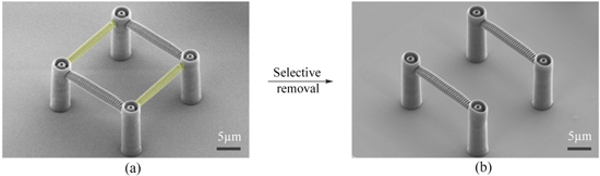
Figure 7. Fabrication of hybrid structures for selective cleavage. (a) The thiol-ene-based network (stained yellow) was integrated into a scaffold written with a standard photoresist. (b) Subsequent cleavage of the integrated structural elements yielded only the unaffected scaffold. [63] John Wiley & Sons. © 2018 WILEY-VCH Verlag GmbH & Co. KGaA, Weinheim.
Download figure:
Standard image High-resolution imageMore flexible control of geometries was performed by a combination of additive TPP and subtractive fs laser multiphoton ablation, by which polymer nanofibers with periodic nanoholes 500 nm in diameter were created [64]. To fabricate polymer nanofibers containing periodic nanoholes, TPP was carried out first. After TPP, subtractive fs laser ablation was employed to form periodic nanoholes in the polymer nanofibers, which acted as Bragg grating structures in the nanofibers. The diameter and the periodicity of the nanoholes were adjustable by controlling the laser irradiation conditions. It should be noted that it is difficult to fabricate such nanofiber Bragg gratings using either TPP or fs laser multiphoton ablation alone. Furthermore, 3D spiral channels inside a polymer cube were fabricated using this technique. The polymer cube was first fabricated using TPP, and 3D spiral channels of 1 μm in diameter were then created at different depths inside the cube by subsequent fs laser multiphoton ablation (figure 8). Figures 8(b)–(d) show optical microscope images of the spiral channels observed at three different focal planes. The spiral channels can be clearly observed at each focal plane. This indicates the ability to form 3D spiral microfluidic channels inside polymer structures fabricated by TPP. This technique enables us to fabricate arrays of spiral microfluidic channels with user-defined spacing (figure 8(e)).

Figure 8. Three-dimensional spiral microfluidic channels inside a polymer cube fabricated by additive TPP followed by subtractive fs laser ablation. (a) Schematic of the 3D spiral microfluidic channel. (b)–(d) An X–Y cross-sectional view of a spiral channel under a transmission-mode optical microscope at different focal planes. The coil diameter of the spiral channel is 20 μm. (e) Array of spiral microfluidic channels fabricated inside a polymer cube with a coil diameter of 5 μm and an interchannel spacing of 3 μm. Reprinted by permission from Macmillan Publishers Ltd: Light: Science & Applications [64], Copyright (2012).
Download figure:
Standard image High-resolution image4.3. Subtractive and additive processing
A combination of subtractive FLAE and additive TPP can create hybrid glass-polymer microstructures. Tičkūnas et al fabricated a cantilever out of fused silica substrate by FLAE and then integrated a polymer beam with the cantilever by TPP to investigate the elastic properties of polymeric microstructures [65]. The mechanical properties of the polymer beam varied, such as Young's modulus, depending on the surrounding solvents, which could be utilized for chemical sensing applications. The same group further applied this hybrid fabrication technique to fabricate lab-on-a-chip devices [66]. Specifically, microchannels were fabricated on the surface of glass by fs laser ablation, where fine mesh filters made of polymer were integrated by subsequent TPP; and the glass substrate was finally sealed with cover glass by fs laser welding.
In principle, welding is unnecessary to create 3D biochips for hybrid subtractive FLAE and additive TPP, since FLAE can directly create 3D microfluidic structures embedded in glass and TPP can integrate 3D polymeric micro/nanostructures into the embedded microfluidic structures. Figure 9 illustrates the fabrication procedure for true 3D biochips using this technique. First, 3D microfluidic structures were created in photosensitive glass by FLAE consisting of fs laser direct writing followed by thermal treatment, HF etching, and a second thermal treatment to smooth the etched surfaces. Then, TPP with a polymer filling, fs laser direct writing, and development was carried out inside the microfluidic structures created by FLAE.

Figure 9. Procedure for fabrication of functional biochips by hybrid subtractive FLAE and additive TPP.
Download figure:
Standard image High-resolution imageThis novel technique has been applied to fabricate biochips possessing functions of micro/nanofiltering, micromixing, and optical sensing [22–25]. One interesting application of biochips fabricated by this technique is the study of cancer cell migration in human bodies [24]. Cancer cells undergo dramatic morphology changes when migrating in confined spaces in human bodies narrower than their diameter during metastasis, and thus it is necessary to understand the deformation mechanism and associated molecular events in order to study tumor progression. The biochip fabricated by this technique accommodates defect-free 3D biomimetic configurations for the observation of prostate cancer cell migration in confined spaces. Specifically, polymeric channels with widths of ∼900 nm, more than one order of magnitude smaller than the cell size, were integrated inside a 3D glass microfluidic structure, as shown in figure 10. It was found that cancer cells with a size of a few tens of μm could migrate in the nanochannels and go through them. More interestingly, the cells first split their bodies into vesicular fragments after migrating through the channels and then fused the divided parts back into single bodies.

Figure 10. Biochip for study of cancer cell metastasis and invasion. Panpipe-shaped scaffold with six polymeric channels with widths of ∼900 nm, which is more than one order of magnitude smaller than the cell size, are integrated inside 3D glass microfluidic structure.
Download figure:
Standard image High-resolution imageAnother scheme of hybrid subtractive and additive processing is selective metallization of 3D glass microfluidic structures [67–69]. In this scheme, fs laser direct write ablation was carried out after fabrication of the 3D microfluidic structures by FLAE using photosensitive glass. The successive electroless metal plating can selectively deposit metal thin films on the ablated glass surface even inside the microfluidic structures. The selective metallization is responsible for the anchor effect at the surface that has been slightly roughened by the ablation. This selective metallization technique was applied to fabricate electrofluidics to manipulate movement directions of aquatic microorganisms in 3D microfluidic structures by controlling the direction of AC electric fields. In the fabricated electrofluidics, two pairs of opposing microelectrodes were formed on the bottom surface of a cross-shaped glass microchannel embedded in glass, as shown in figure 11(a). When the Euglena cells were introduced into the chip, random swimming behavior was observed (figure 11(b)). The direction of the AC electric field can be controlled by appropriately choosing the pairs of electrodes between which the electric voltage is applied. Then, 2D orientation of cell motions can be achieved in the microfluidic environment, as shown in figures 11(c)–(e).

Figure 11. (a) Photograph of the electrofluidic device in which two pairs of opposing microelectrodes are formed on the bottom surface of a cross-shaped closed glass microchannel for 2D electromanipulation of Euglena cells. The inset is a tilted view of the same chip, showing the preparation of continuous metal structures from inside of the microchannel to the glass chip surface. Swimming behaviors of Euglena cells in a microfluidic environment (b) in the absence of an electric field and under an applied electric field (20 Vp-p, 0.8 MHz) between electrodes (c) '1 and 3' and (d), (e) '1 and 3' and '2 and 4'. (c)–(e) Represent, respectively, 90°, +45°, and −45° orientations of cell motion with respect to the x-axis. 'ON' and 'OFF' correspond to experiments with and without electric power, respectively. The numbers in gray in (b), (c) indicate that no AC voltage was applied. The numbers in yellow and red in (c)–(e) represent the opposite polarities. The blue arrows in (c)–(e) indicate the directions of the electric field. The scale bars in (b)–(e) indicate 200 μm.
Download figure:
Standard image High-resolution image4.4. Subtractive, additive, and subtractive processing
The successive procedure of FLAE, selective metallization, and formation of fs laser-induced periodic surface structures (fs-LIPSS) enables us to fabricate highly sensitive 3D microfluidic surface-enhanced Raman spectroscopy (SERS) chips [70]. The fabrication of 3D microfluidic SERS chips includes three main steps, as illustrated in figure 12. In the first step, a 3D microchannel is fabricated in a photosensitive glass substrate by subtractive FLAE (figures 12(a) and (b)). The second step is selective metallization of the copper-silver (Cu-Ag) layered thin film inside the microchannel (figures 1(c) and (d)). Copper deposition is necessary to ensure strong adhesion of the metal thin films to the glass substrate, while Ag is one of the most suitable metals for SERS sensing. The final step is the formation of a periodic metal nanostructure by fs-LIPSS (figure 1(e)). It is well known that the interactions of linearly polarized fs laser pulses with a material can form a nanometer-sized parallel periodic structure, typically referred to as LIPSS [71, 72]. The period of LIPSS is 1/2–1/10 of the laser wavelength, depending on the materials and the laser irradiation conditions; and the orientation of LIPSS is perpendicular to the polarization direction of the laser beam. To create a two-dimensional (2D) array of metal nanodot structures, the sample was rotated by 90°. The laser scan was repeated over the entire metal film deposited on the bottom of the microfluidic channel embedded in the glass after the first laser scan, representing a double exposure. The double exposure created a 2D nanodot array with an average width of 200 nm. More importantly, the distance between each nanodot was measured to be approximately 50 nm, which could efficiently enhance the electromagnetic field for SERS sensing due to the generation of hot spot effect. The fabricated microfluidic SERS chip showed high performance with an enhancement factor as high as 7.3 × 10⁸ along with a relative standard deviation as small as 8.88%. One potential application for the SERS chip is the detection of trace levels of toxic substances in the environment. Thus, detection of cadmium (Cd), which is one of the most toxic elements and is widely found in fertilizers, engine exhaust, plastics, and other industrial products, has been demonstrated. It was previously reported that the presence of Cd significantly affects the Raman peak intensity of crystal violet (CV) SERS bands [73]. Specifically, the CV Raman peak intensities drastically decreased with the addition of even very low concentrations of Cd. The intensity change can be thus utilized for measurement of Cd concentrations. The Raman spectra of 10−5 M CV solutions with different concentrations of Cd2+ (from 10 ppb to 10 ppm) were, therefore, analyzed. Figure 13(a) presents the spectra, which exhibited primary peaks at 525, 761, 803, 916, 976, 1175, 1302, 1375, 1443, 1473, 1532, 1585, and 1620 cm−1, all of which decreased in intensity with increasing Cd2+ ion concentration. The detection limit of Cd2+ by this measurements was evaluated to be as low as 10 ppb. Finally, the real-time SERS sensing of Cd2+ solutions with concentrations of 0.01, 0.1, 1, and 10 ppm has been successfully demonstrated as shown in figure 13(b).

Figure 12. Procedure used to fabricate a 3D microfluidic SERS chip by all-femtosecond-laser-processing, including (a), (b) FLAE, (c), (d) selective metallization of 3D glass microfluidic structure, and (e) fs-LIPSS processes. (f) 2D nanodot metal array fabricated by a double exposure of a lineraly polarized fs laser beam.
Download figure:
Standard image High-resolution image
Figure 13. (a) Raman spectra of CV solutions (10−5 M) with varying concentrations of Cd2+ on a 2D periodic Cu-Ag nanostructured SERS substrate and (b) the intensity of the 10−5 M CV Raman peak over time while injecting Cd2+ solutions having various concentrations (inset: the magnified image of a region circled with a red dashed line from 0.01 to 1 ppm.).
Download figure:
Standard image High-resolution image
5. Summary
The fs laser is a powerful tool for fabricating 3D micro/nanostructures. The most significant feature of fs laser 3D processing is that it offers three different schemes, undeformative, subtractive, and additive processing, the first two of which are not accessible by other existing techniques. Each scheme, however, exhibits different advantages and drawbacks. Meanwhile, a combination of different schemes offers the capability of fabricating more complicated geometries of 3D structures with finer resolutions, thereby ensuring more functionality and more diverse applications. Researchers have succeeded in fabricating functional biochips, including nanofluidics, optofluidics, and electrofluidics, chemical sensors, microfluidic SERS chips, and so on. Thus, the hybrid concept opens a new avenue for manufacturing based not only on fs laser processing but also other conventional machining techniques. Finally, it can be concluded that the demand for hybrid fs laser 3D processing will continue to increase, and higher degrees of functionalization and integration into micro/nanosystems will be achieved.