
Abstract
Two-dimensional (2D) materials have revealed many fascinating physical and chemical properties. Due to the quantum confinement and enhanced many-body effects especially the optical properties are altered compared to their bulk counterparts. The optics of 2D materials can easily be modified by various means, e.g. the substrate, doping, strain, stacking, electric or magnetic fields. In this review we focus on the theoretical description of the excited states and optical properties of 2D semiconductors paying particular attention to the current challenges and future opportunities. While the presented methodology is completely general and applicable to any 2D material, we discuss results for the transition metal dichalcogenides, their heterostructures, and some novel materials from the computational 2D materials database.
Export citation and abstract BibTeX RIS

Original content from this work may be used under the terms of the Creative Commons Attribution 4.0 license. Any further distribution of this work must maintain attribution to the author(s) and the title of the work, journal citation and DOI.
1. Introduction
Two-dimensional (2D) materials are crystalline, covalently bonded, and chemically inert sheets of atoms that measure just a few angstroms in thickness, but can have lateral extensions in the micro- or millimeter range. Such materials can be exfoliated from layered bulk materials or synthesised bottom-up using e.g. chemical vapour deposition or pulsed laser deposition. In 2D materials, the confinement of electrons to the atomically thin layers result in highly anisotropic properties. For example, in-plane bonds are typically strong and covalent or ionic, while weak van der Waals bonds act in the out-of-plane direction. This anisotropy is also reflected in the electronic and optical properties and eventually leads to many interesting phenomena such as valley polarization, charged excitations, quantum confinement, hyperbolic response, etc [1].
There are many two-dimensional materials; more than 50 have been synthesised or exfoliated in monolayer form while many hundreds are predicted to be exfoliable from already known layered bulk compounds [2, 3]. Several materials have been used for a long time in their bulk forms in which hundreds of layers are stacked on top of each other. For instance, minerals like graphite or MoS2 have been known since thousands of years [4] and their atomic structures have been clarified several decades ago [5, 6]. Although techniques for cleaving and thinning are well established, it took until 2004 for graphite to be first observed in its monolayer form graphene [7–9]. In the following years, many further materials such as the monolayers of several transition metal dichalcogenides (e.g. MoS2 [10]) or black phosphorus [11] have been observed experimentally.
In particular, conventional semiconductors like silicon or gallium arsenide have been studied intensively long before two-dimensional materials, e.g. due to their relevance for modern computer technology, integrated electronics, or solar cells. Silicon has been used in most information technology devices in daily life for more than 50 years. Because of its indirect band gap, efficient coupling of electronic and optical properties is challenging and silicon has a vanishing gap in its two-dimensional phase [3, 12]. However, this long-standing attempt promises easier interfacing with today's fiber optic communications and faster and more parallel information processing. Due to the reduced dimensionality, light-matter interactions in many two-dimensional materials are stronger than in their three-dimensional counterparts [1, 13]. This also makes them promising candidates for renewable energy and sustainability applications (e.g. solar cells or light-emitting diodes).
A fundamental understanding of light-matter interactions at the atomic length scale is mandatory for targeted development of novel and improved opto-electronic devices. In this work, we will theoretically investigate the optical properties of various two-dimensional materials and different ways to modify them. All investigations will be performed using ab initio techniques which allow for a parameter-free prediction of the corresponding physical properties and even the prediction of novel hypothetical materials. These highly accurate and system-independent methods are accompanied by a high numerical cost, i.e. highly efficient implementations in computer programs for supercomputers are required. They develop their full potential gaining new physical insights in combination with experimental observations. The detailed theoretical analysis allows clarification of the physical mechanisms involved, and at the same time the experiments verify the theoretical predictions.
We start this work with a brief overview of the state-of-the-art ab initio techniques in section 2. The starting point is the well established density functional theory (DFT), explicitly corrected by van der Waals interactions, which are not well described by the standard functionals. The variational principle can be used to determine the lowest total energy and the corresponding density for the ground state of a system. The minimal energy with respect to the atomic positions determines the optimal structure. The electronic and optical properties require a more accurate description including excited states and are today mostly based on many-body perturbation theory. Single particle processes such as band structures can be approximated very reliably by single-particle Green functions and their equation of motion in the GW approximation. Optical properties are described by the transition between two different electronic states preserving the number of particles. Consequently, their description requires the two-particle Green function and its equation of motion (the Bethe–Salpeter equation). Due to the electron–hole interaction, bound excitons can form and significantly change the spectrum. Moreover, three-particle excitations (trions) are important for many naturally doped 2D materials and lead to additional red-shifted peaks. Their theoretical description requires a rigorous quantum mechanical treatment, but is often missed in simulations. We conclude the section with novel theoretical approaches to evaluate the influence of magnetic fields on electronic and optical properties.
In the following sections we investigate the optical properties and different ways to modify them in detail. Figure 1 summarizes several external stimuli which can be used in two ways: On the one hand, these modifications are suitable to design the optical properties, and on the other hand, they provide insight into the physical nature of the underlying excitations. In section 3, we begin the discussion of monolayers of transition metal dichalcogenides and examine their characteristic optical spectra. Due to the electronic band structure, the low-energy excitations mostly originate from transitions close to the ±K valleys. In addition to the large exciton binding energies, which include a Rydberg series of excitons, the strong spin orbit coupling leads to two excitons with similar amplitudes. We take a closer look at possible excitations which do not couple directly to optical measurements. Such excitations may be dark due to the character of the wave function, e.g. if the spin of the electron and hole are reversed. Especially in transition metal dichalcogenides with their large spin orbit coupling of the valence bands, but energetically very close conduction bands, there is a close competition which state is the energetically lowest. If the difference of the momenta of both particles, electron and hole, is larger than the momentum of the photon, no optical transition is possible in the first place. However, the momentum can be transferred to a phonon and an assisted optical transition is possible, for example in photoluminescence experiments. In this work we focus on the calculation of the momentum-dependent exciton dispersions. We also investigate the modification due to a possible substrate. While such a substrate is artificial in our calculations, it is always present in experiments, and thus modifying the substrate is the most fundamental way to change the optical response.

Figure 1. Possible modifications to tune and design optical excitations in 2D materials. Apart from that, these stimuli can be used to investigate their properties.
Download figure:
Standard image High-resolution imageSection 4 introduces another common perturbation in 2D materials, the doping. In many experiments, samples are unintentionally doped with additional electrons. On the other hand, the doping can also be tuned intentionally if a voltage is applied. In our theoretical calculations we assume small doping concentrations, which allows us to neglect the influence on the band structure and limit ourselves to three-particle correlations. A bound state (trion) can appear below the corresponding exciton. This is not only true for the lowest energy transition, but we have also been able to discover trions for the second Rydberg state.
Due to mismatch of the lattice constants or imperfections in the sample preparations 2D materials may naturally be strained locally or on a larger scale. Strain can also be selectively tuned by bending the substrate. In section 5 we investigate the influence of the electronic and optical properties from first principles by modifying the structural properties. Biaxial strain can be simulated by changing the lattice constant, while uniaxial strain also distorts the structure and breaks the hexagonal symmetry. The resulting structural changes shift the bands according to the composition and symmetry of the corresponding wave functions. At small strain values an almost linear response can be observed, which is characteristic for each band. As a consequence, the excitation energies of the excitons exhibit characteristic shifts that can be used to identify them. On the other hand, a sufficiently large strain may even be utilized to change the energetic order of the excitons.
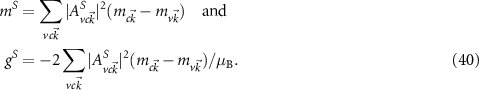
Two-dimensional materials are almost only surface. Like any other material, they have a certain concentration of defects. Additional atoms and molecules can adsorb both at the defect-free areas and at defects sites. Section 6 examines the properties of some exemplary molecules. On the one hand, we have chosen an oxygen molecule which has a triplet ground state, making it one of the simplest examples of a magnetic molecule. Even if the material is inert, a weak van der Waals bond can form, and a certain overlap is observed. This changes the electronic and optical properties of the monolayer and depends on the spin character of the molecule. On the other hand, vacancies and the adsorption of different molecules therein are studied. Several molecules are able to recover the defect-free properties of the 2D material very well.
Section 7 introduces the stacking of individual layers to form homo- or heterostructures. Several 2D materials exist in such naturally layered three-dimensional structures, e.g. graphene, hexagonal boron nitride or MoS2. In addition, it is possible to build artificial structures like twisted homobilayers or heterostructures. Even if the layers are connected only by van der Waals interaction, several interesting phenomena can be observed. For example, a monolayer of transition metal dichalcogenides shows a direct band gap, while multiple layers have indirect band gaps. Besides the resulting changes of the optical spectrum, spatially indirect states are present on different layers which have no counterpart in a monolayer. Such interlayer excitations consist of a hole and an electron on two different layers and are the analog to charge-transfer states in molecules. In particular, in systems where interlayer excitons are the ground state, their long lifetime might be promising. The level alignment of the different layers can also be utilized to distinguish interlayer states from other excitations by employing a perpendicular electric field. A further interesting question concerns the changes of the excitations due to additional doping, i.e. interlayer trions.
In section 8 we calculate the response of the electronic and optical properties due to an external magnetic field. While the use of electric fields orthogonal to the layer is conceptual simple in the supercell method, magnetic fields break the translational symmetry in the layer and seem to prohibit the applicability of our periodic calculations. However, by using Berry phase techniques the problem can be reformulated and the band- and  -dependent shifts can be evaluated. By employing the Bethe–Salpeter equation, we can connect such shifts to the shifted exciton energies and eventually to the changed optical spectrum. Even if magnetic fields probably have the smallest absolute impact, they can still be used to split excitons with different character, e.g. the ±K valleys in transition metal dichalcogenides.
In section 9 we consider the central object, the two-dimensional material itself, from a broader perspective. After presenting a high-throughput screening approach for the discovery of novel hypothetical materials, we address the statistics of some material properties like band gaps or exciton binding energies. The large set of systems with very diverse physical and chemical properties is also an ideal test set to compare different methods, such as those discussed in the first section.
2. Theoretical methods
A quantum mechanical system can be described by the Schrödinger equation or, more generally, by the Dirac equation. In the time-independent case this is given by  , where E are the energies and Ψ are the wave functions. While the Hamiltonian
  is known exactly even for systems with macroscopic extent, the direct solution for
  particles is out of scope (even after the ionic motion is decoupled via the Born–Oppenheimer approximation). Different concepts have been developed to rewrite the problem, followed by different approximations, of which the two most commonly used are presented here: The DFT, or more precisely the Kohn–Sham scheme of DFT, models the interacting electron system as a non-interacting system moving in an effective potential, and is well suited for calculating the ground state and related properties. Many-body perturbation theory (MBPT) provides a systematic way of accounting for the two-body Coulomb interaction beyond the mean-field level, by summing certain subsets in the perturbation series to infinite order. In this way, it is possible to obtain an accurate description of the optical excitations. Thus, the combination of both techniques is a suitable set of tools to describe and predict the physical properties in this work.
After a brief summary of the two techniques in sections 2.1 and 2.2 and the practical aspects in section 2.3 (for a more detailed discussion, we refer the reader e.g. to [14–17]), the new developments for doping (trions) are discussed in section 2.4 and for magnetic fields (Zeeman shifts) in section 2.5.
2.1. DFT
Similar to the previously developed Hartree–Fock theory [18, 19], the Kohn–Sham scheme of DFT is an effective one-particle description in the mean field of all other particles. Hohenberg and Kohn have proven [20] that the ground-state energy and the wave function are related to the density 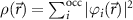 by a unique functional. By varying them, the ground state density
  can be found for which the functional derivative becomes zero. Eventually, the effective one-particle equation for the ith particle (wave function
  and energy εi
) is
and energy εi
) is
which is the so-called Kohn–Sham equation [21]. The effective potential mediating the interaction to all other electrons is given by the Coulomb interaction to all electrons, the interaction with the external potential (of the nuclei), and the functional derivative of the exchange-correlation (xc) potential

The solution has to be found self-consistently, since the input density is composed of the resulting wave functions. The quality of the formally exact DFT depends on the quality of the functional. For solid state systems, the local density approximation (LDA) [22, 23] or the generalized gradient approximation (GGA) [24, 25] are typically chosen since they systematically exploit the dependencies of  and
and  . While εi
are strictly the Lagrange multipliers, in practice the interpretation as single-particle excitation energies and band structures is often a reasonable first approximation. The latter can be improved (somewhat empirically) by mixing the non-local exchange potential with the local GGA potential leading to the so-called hybrid functionals [26]. For HSE06 [27], for example, we have observed an improvement of about 20% for the band gaps of 2D materials [3]. Unfortunately, HSE06 still underestimates the band gaps by more than 20%, and further systematic improvements of the functional are challenging. Another drawback is the lack of weak but long-range van der Waals-type interactions. Methods to correct for these interactions are summarized, e.g. in [28].
. While εi
are strictly the Lagrange multipliers, in practice the interpretation as single-particle excitation energies and band structures is often a reasonable first approximation. The latter can be improved (somewhat empirically) by mixing the non-local exchange potential with the local GGA potential leading to the so-called hybrid functionals [26]. For HSE06 [27], for example, we have observed an improvement of about 20% for the band gaps of 2D materials [3]. Unfortunately, HSE06 still underestimates the band gaps by more than 20%, and further systematic improvements of the functional are challenging. Another drawback is the lack of weak but long-range van der Waals-type interactions. Methods to correct for these interactions are summarized, e.g. in [28].
In general, DFT has been very successful in predicting structural and thermodynamic properties of materials while its description of excited states has not been satisfactory, and can most be taken as a starting-point for more advanced treatments such as MBPT. The calculations of optical properties from standard DFT, however, do not lead to reasonable predictions. To achieve this, the time-dependent generalization (TD-DFT) can be used [29–31], in which the adiabatic LDA (ALDA) is routinely applied for the exchange-correlation potential. Unfortunately, several shortcomings remain, especially for extended systems [16, 32]. These can be overcome using many-body perturbation techniques.
2.2. Many-body perturbation theory
In many-body perturbation theory (MBPT), the discussion starts from the many-body ground state  [33]. Using the shorthand notation for position, spin, and time
  and atomic units (i.e.
  ,
,  , and
, and  leads to lengths in aB and energies in Ry), the causal one-particle Green function is given by

It describes the creation of an electron at 1, its propagation and annihilation at 2, or vice versa.  is the time-order operator which adds a negative sign when
  and
and  are field operators for the annihilation (creation) of an electron that can be expressed as
  .
.  denotes the creation of an electron in the ith state and ϕi
the corresponding wave function.
denotes the creation of an electron in the ith state and ϕi
the corresponding wave function.
The equation of motion for the Green function

where VCoul is the Hartree potential, links the one-particle Green function to the two-particle Green function G2, and we eventually find an infinite hierarchy of equations. The hierarchy can be broken by introducing the self-energy 

In principle, the self-energy can be obtained self-consistently by five equations, the so-called 'Hedin's equations' [33]:


Equation (6) is the Dyson equation that links the Green function to the non-interacting G0 and the self-energy Σ. The latter is determined (equation (7)) by the screened Coulomb interaction W and the vertex function Γ ( means the evaluation at
  ). W can be calculated from the bare Coulomb interaction
  and an additional term including the polarizability P. P in turn depends on G and Γ. The most complicated form is obtained for the vertex function (10), which also includes a functional derivative of the self-energy Σ.
Although Hedin's equations provide a formally exact framework for obtaining Σ, practical calculations require approximations. Often, the GW approximation is applied. This approximation starts from  in equations (6) and (10) and the self-energy simplifies to

W can be calculated via the dielectric function in the random phase approximation 
 , with
  . For the frequency integration (after a Fourier transformation from the time domain), a simple plasmon-pole model [34, 35] is used. Finally, the wave function
  and energy
  of the quasi-particle (m includes its spin) can be calculated by

Since Σ depends on  and
and  , solving equation (12) would require another self-consistency. However, due to the simplified vertex in the GW approximation self-consistency may actually worsen the results [36, 37], so we stick to updating the wave functions and energies based on DFT. The energy dependence of the self-energy is approximated as

and  denotes the renormalization constant including the derivative of the self-energy with respect to the energy.
  describes the spectral weight of the corresponding quasi-particle and its value is typically around 0.7 [38]. Transformed to
  space, we can finally calculate

and diagonalize  . The solution is found when
  agree on the left and right sides of this equation and lets us identify the corresponding wave function
  . While this treatment is important in many heterogeneous systems [39, 40], in other cases non-diagonal elements are less crucial and the solution simplifies to
  with
with  . In this case the linearized form is given as
  . We note that the vertex corrections in general have relatively small effect on the QP band gap while they tend to up-shift the absolute band energies (relative to the average potential) [41, 42].
Equation (14) illustrates that only the difference of the self-energy and the exchange-correlation potential is important. Based on the observation that a fictitious metallic screening reproduces the LDA  for many systems, an alternative approximation is possible [43, 44]
This  approximation allows to focus on the changed screening with respect to the LDA. Such changes are usually more than an order of magnitude smaller than the original quantities. This allows us to avoid the time-consuming RPA calculation of the dielectric functions and apply RPA-parametrised model functions [45]. In particular, we have found good agreement for 2D materials [44, 46], and we refer the reader to these works for further details.
Until now, we have focused on single excitations that can be described by the Green function  . To understand the optical properties of materials, a detailed understanding of the correlated electron–hole excitations is necessary [16, 47], i.e. G2 and its equation of motion, the Bethe–Salpeter equation (BSE) introduced by Strinati [48, 49]. Unlike the one-particle Green function, which mediates between the N and
  particle system, G2 contains electron–hole pairs (we neglect possible hole-hole or electron-electron pairs). The ground state
  can therefore be excited by the creation and annihilation operators of G2 to a state S, denoted
  , without changing the number of particles. The two-particle Green function is defined analogously to equation (3) as

For excitons, we can assume that an electron–hole pair is created at times t1 and  and annihilated at t2 and
  . We note that G2 and the corresponding correlation function L are four-point functions

Its equation of motion, the BSE is given by

where  describes the non-interacting case and
  is the interaction kernel (electron–hole interaction). After the transformation to the energy domain and to two effective particles, the BSE can be rewritten as a generalized eigenvalue problem
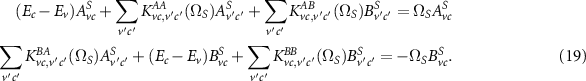
 are the energy differences of valence and conduction bands and K are the corresponding matrix elements of the interaction kernel

(for KAB
, KBA
and KBB
the structure is similar, but the arguments are interchanged). Employing the GW approximation, the exchange part is the bare Coulomb interaction while the direct part is screened by the dielectric function  . By solving equation (19) we can find the exciton energies
  and the amplitudes AS
and BS
of the excitations and de-excitations
and the amplitudes AS
and BS
of the excitations and de-excitations  .
.
Many studies have found that neglecting KAB
(i.e. setting  ) leads to reasonable results for extended semiconductors; this procedure is known as the Tamm–Dancoff approximation [50]. Following this route leads to the more compact form

where the dimension of the eigenproblem can still become large, given by the product of the hole and electron bands and the number of  points considered. Since spin–orbit coupling plays an important role in many 2D materials, the Hamiltonian does not have a block structure and does not decomposes into singlet and triplet states [16, 47].
The optical properties of a material are measured via the macroscopic dielectric function [16], which depends on the energy ω and the direction of the limit 

For ω = 0 the dielectric constant ε0 is obtained. Because the absorption spectrum is given by the imaginary part ( ), we will focus on
  in this work. To evaluate the coupling to the light field, we calculate the imaginary part
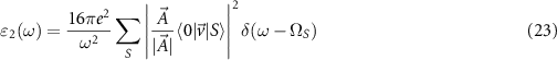
as the sum of all possible excitonic states whose weights are determined by the normalized polarization of the light  (we assume a linear polarization) and the velocity matrix elements. These elements can be calculated as
  , therefore both required values (the excitation energies
  and the electron–hole amplitudes
  ) are known after diagonalizing the BSE Hamiltonian.
2.3. Some practical aspects
After the theoretical derivations in the last sections, the actual calculations have to be performed numerically on a computer.
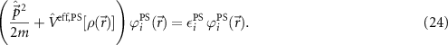
The first approximation that is typically applied is the introduction of pseudopotentials (PS) [51–54] and corresponding wave functions. The basic idea is to add the inner electrons to the potential of the nuclei (because they are not relevant for chemical bonds etc) and treat only the valence electrons explicitly. By this procedure, equation (1) can be rewritten as
Moreover, this allows the spin–orbit coupling [55] to be taken into account without having to solve the Dirac equation for the entire system.
In addition, the wave functions have to be treated numerically. For most calculations we use atom-centered Gaussian orbitals. The advantage of Gaussian orbitals is their short-range behavior in real and reciprocal space and the analytical solution of their integrals. Each function consists of several orbitals with decay constants γ (denoted by the index α including their s-, p-, d-character, etc) at 
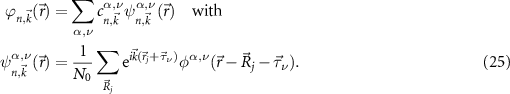
For details and an efficient numerical implementation, we refer to [56, 57]. The coefficients  are obtained by the solution of the eigenvalue problem

involving the overlap matrix S in addition to the Hamilton matrix H.
The two-point quantities in equation (11) have to be calculated with an auxiliary basis β, e.g.  . The required three-center integrals

use the Gaussian orbitals  from DFT and again Gaussian orbitals or plane waves for
  [58]. In particular, the GdW allows for a small number of auxiliary basis functions (plane waves) and enables many of the calculations discussed in the following. For example, periodic supercell calculations up to about 100 atoms are possible. Another critical aspect is the convergence of the supercell size when employing the GW/GdW approximation in a 2D material (in a 3D periodic code). Due to the long-range character, an inversely proportional extrapolation to infinite cell sizes is required; for details and the discussion of convergence see [44].
In addition, we use GPAW [59, 60] for several calculations. This code is based on the Projector Augmented Wave (PAW) method [61] which is as a generalized pseudopotential method. Already at the DFT level, we employ a plane wave basis. For further details we refer to [3].
2.4. Three-particle states
The theoretical approach described in section 2.2 has been developed for neutral semiconductors. In the case of doping, this is no longer strictly correct. The electron and the corresponding hole created by the excitation with light can bind to a third particle (an additional electron or hole in n- and p-doped systems, respectively).
The treatment of three-particle states requires the description of three independent quasi-particles. The description as an exciton with a 'small' perturbation is often insufficient because both electrons or holes are indistinguishable. In principle, this would lead to the three-particle Green function G3 and the solution of its equation of motion. To the best of our knowledge, the complete formal derivation has not been presented in the literature and seems to be out of reach. Here we will approximate the three-particle Hamiltonian similarly to the BSE. This approach has been adopted by Tempelaar and Berkelbach [62], Torche and Bester [63], and Zhumagulov et al [64].
In second quantization the many-body Hamiltonian is given as

where the matrix elements of the single-particle terms (kinetic energy and external potential) are hij
and the matrix elements of the Coulomb interaction are  . In a periodic system each index has to be understood including the momentum
  . Within Hartree–Fock theory, the single-particle states
  are the solutions of the Hartree–Fock equations, and the matrix elements can be calculated by

where  and the bare Coulomb interaction is
  . For an electron–hole pair configuration
  the matrix element is

with  being the band-structure energy and
  the ground-state energy. Note that equation (30) is not diagonal and the diagonalization of the Hamiltonian

leads to the excitation energies  and the excited states, which are linear combinations of the free electron–hole pair configurations
  . In the last section we found a very similar form using many-body perturbation theory, i.e. after the Tamm–Dancoff approximation in equation (21). However, two important changes can be concluded: First, the energy levels from Hartree–Fock are replaced by those from GW and second, the direct interaction is screened by the dielectric function of the system
  .
.
For the three-particle states, we take a similar route. For the configurations of two electrons and one hole  (
( ), we can derive the matrix elements within Hartree–Fock [65, 66]
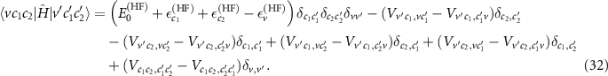
In addition to the independent motion of each of the three particles, the two body interactions between each pair of particles are included. In analogy to the BSE, we replace V → W in the direct term of the electron–hole interaction and for the interaction of both electrons (last terms). To ensure invariance when changing c1 and c2, both terms are screened. Finally, we find the matrix elements
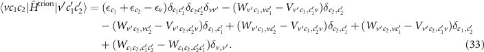
and by diagonalizing the corresponding Hamiltonian

we can calculate the energy of the trions  and their wave functions

for trions T with momentum  . Because of momentum conservation, the wave numbers of
  have to satisfy
  . Note that the trion in an optical spectrum is not found at the trion energy
  , but at the transition energy

as an electron remains in the conduction band  (or is already present before absorption). Note that the
  points in equation (33) are responsible for both, the convergence as well as the applied doping. As discussed in previous works, our results should be understood in the limit of vanishing doping [67].
2.5. Magnetic fields
The general treatment of electro-magnetic fields in a periodic calculation is challenging. Corresponding to the electric and magnetic fields  and
and  , the (vector) potentials ϕ and
  can be determined by
  and
and  . These potentials ϕ and
  enter the Hamiltonian, and if they are not only varying vertical to the 2D material, the lattice periodicity is destroyed. To overcome this in magnetic fields, Kohn [68] and Roth [69] have reformulated the theory around the 1960s, as did Chang and others later using Berry phase techniques [70–74]. Although several effects of a magnetic field on optical absorption have been measured and theoretically modeled over the years, a predictive theoretical method was lacking. In the following, we show a first step in this direction [75].
Building on the ideas of Kohn and Roth, we solve the Hamiltonian without a field 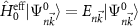 (see section 2.1). In a next step, we include the magnetic field (along the out-of-plane z-axis) as a perturbation
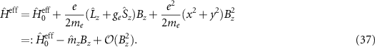
Here  and
and  are the angular momentum and spin operators, respectively, where we assume that
  can be evaluated at the position of our local basis functions. For small fields, we only need to consider the linear term in B (we omit z for brevity), and the magnetic moment is given by an orbital and a spin contribution
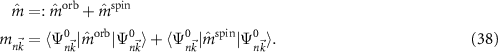
The destroyed lattice periodicity is reflected in the spatial dependency of the angular momentum operator  which prohibits a direct evaluation. Therefore, we follow the derivation of Chang and Niu [70] for the magnetic moment of a wave packet

where  is the lattice periodic part of the wave function and its derivative is evaluated as finite difference. Since the spin part of equation (38) can be calculated straight forward, this allows the study of the changes of the electronic states for small fields.
To investigate the changes of the optical properties, we have to take into account the wave function of the excitons. This can be evaluated from the BSE (19). Consequently, the shift mS of each exciton S can be evaluated by
The g factor of the exciton S is often related to the difference of corresponding experimental measurements with  circularly polarized light
  [76]. Because the effects are reversed for different helicities, the factor −2 in equation (40) is obtained. If excitonic effects were neglected, the g factor of the transition from (
 ) to (
 ) could be approximated by

The theory presented in this section focused on the case of weak magnetic fields, and will be applied in section 8. For stronger magnetic fields, the diamagnetic term and the formation of Landau levels, i.e. effects beyond linear response, become important.
3. Excitations of free-standing 2D materials and substrate screening
A particularly well-suited class for the investigations of opto-electronics properties are the group-6 transition metal dichalcogenides (TMDCs) MX2 (M = Mo/W, X = S/Se/Te) for which many experimental results are available [77]. For this reason we will mainly focus on the TMDCs in the following sections. Some electronic and optical properties of other 2D materials will be studied in section 9.
TMDCs consist of three atoms per unit cell: one transition metal in the central plane and two chalcogenides above and below. A side view of the hexagonal structure is shown in figure 1 for MoS2. The following discussions are based on calculations employing the experimental lattice constants, which are close to the theoretically optimized ones [78]. After we have discussed the ground- and excited-state properties of free-standing monolayers in vacuum, the influence of the substrate is analysed and is shown to provide a simple, yet efficient means to tune the properties of the 2D material.
3.1. Free-standing monolayers of transition metal dichalcogenides
Electronically the TMDCs are semiconductors with indirect band gap in the bulk or for several layers, while they have a direct band gap in the monolayers. Figure 2 shows the band structures of MoS2 and WSe2 along a path through the high-symmetry points Γ, M, and K. The dashed lines show the results of DFT-LDA, that clearly underestimate the band gaps compared to our MBPT calculations within the GdW approximation. The latter reveal direct band gaps of 2.89 and 2.44 eV at the K point. Both values are in reasonable agreement to experimental measurements of 2.72 and 2.56 eV [79]. The large difference to the DFT band gaps of 1.78 and 1.65 eV (quasi-particle correction) is the result of the reduced screening in two-dimensional materials (in bulk, the direct gap in MoS2 is 2.19 eV and the quasi-particle correction is less than half the size [80, 81]). The smaller the screening, the larger the inaccuracy of the DFT-LDA which is based on the homogeneous electron gas. In figure 2, the red and blue colors denote the spin polarization  and exhibit a clear out-of-plane polarization (i.e. orthogonal to the layers). The highest valence bands (VBs) and the lowest conduction bands (CBs) are polarized by more the 90% (often nearly 100%) at the band extrema. In particular, the VBs are distinctly split, which can be traced back to the strong spin–orbit coupling. Due to the heavier elements in WSe2, the VBs are split by 570 meV, while the value for MoS2 is only 180 meV. The CBs show an interesting characteristic close to the K point. They approach each other, and in the case of Mo-based TMDCs, they even change order. A corresponding schematic sketch is shown in the right panel of figure 2.

Figure 2. Comparison of the quasi particle and DFT band structures of MoS2 and WSe2 monolayers. The GdW is indicated by black and colors, LDA is dashed gray. The size of the added points is proportional to the expectation value  (spin up in red, spin down in blue). The insets show a zoom in of the CB at K. The bottom panel shows a schematic sketch of the band structures and the corresponding Brillouin zone. Reprinted figure with permission from [44], Copyright (2018) by the American Physical Society.
Download figure:
Standard image High-resolution imageThe low-energy part of the optical spectrum is mostly governed by the transitions from the highest VBs to the lowest CBs. Due to the Coulomb interaction between the excited electron and the generated hole, peaks with strong optical weight can be found below the corresponding band gaps in figure 3. The lowest peaks are called A excitons and have, with respect to the band gaps, exciton binding energy of 0.76 eV and 0.68 eV, respectively. For bright excitons the spin of electron and hole have to be the same, i.e. in the absorption spectrum only transitions between bands with the same color in figure 2 can occur. Therefore, the next bright exciton B stems from the bands with different spin. The splitting between A and B follows the large spin-orbit splitting of the VBs and is thus stronger in WSe2 compared to MoS2. Furthermore, peaks with lower optical weight corresponding to excited states (A , B
, B ) are observed. Similar to possible excitations in a hydrogen atom, excitons can also form a Rydberg-like series [83, 84].

Figure 3. Absorption spectra of MoS2 and WSe2 monolayers. Below the band gaps of 2.89 and 2.44 eV, several clear peaks can be identified, labeled A, B, and C, respectively. The corresponding higher excited states are denoted as A etc where the notation as 2s corresponds to the symmetry of the excitonic wave function. The lowest excitations are optically dark and are therefore labeled D. Reprinted figure with permission from [44], Copyright (2018) by the American Physical Society. Reprinted figure with permission from [82], Copyright (2017) by the American Physical Society.
Download figure:
Standard image High-resolution imageA detailed understanding of the excitations is possible by analyzing their wave functions. In figure 4(a), the A exciton in MoS2 is shown in real and reciprocal space. When the hole is fixed at the central Mo atom, the probability to find an electron is significant in a circular region of about 20 Å in diameter. The Fourier transformation relates this to the reciprocal contributions which are significant around the ±K points. For WSe2 the comparison between dark and bright excitons is shown in figure 4(b). While their spatial extent is similar (but not identical, not shown here), the corresponding conduction bands have different spin character, and the selection rules forbid that spin flip processes are bright. Due to the energetic position of the bands in WX2, the appearance of D as the lowest state is not surprising. Interestingly, also in MoS2 the transition to the second-lowest conduction band leads to a dark exciton D below A. We find that the reason for this is a combination of three tiny differences: (1) The effective mass of the bands is different, (2) the exchange interaction is absent for D, and (3) the slightly different exciton wave functions also lead to small differences of the direct interaction [82]. Experiments [85] have proven that dark excitons are the ground state for MoS2, WS2, and WSe2. For MoSe2 the optically active and dark states are close in energy. Further details of the calculated energetic alignment can be found in table 1 of [82].

Figure 4. (a) Modulus squared of the exciton wave function of the A exciton in MoS2 in real space on the plane spanned by the Mo atoms (blue dots). The position of the hole is fixed in the center. The modulus of the contribution to the exciton in  -space
  is shown below. (b) Comparison of the contribution of the D and A excitons in WSe2, on top of the bands from figure 2. Reproduced from [78]. CC BY 4.0. Reprinted figure with permission from [82], Copyright (2017) by the American Physical Society.
Download figure:
Standard image High-resolution image3.2. Finite-momentum exciton landscape
After the optically bright exciton and the spin-forbidden dark states have been introduced, we now discuss the characteristic of excitons whose momentum is much larger than that of a photon. Consequently, all transitions are dark in the absence of additional momentum transfer by phonons or the like.
In figure 5, we examine possible excitations for different momenta. We restrict ourselves to Q pointing in the y direction in figure 5(a). These momenta can be used in the general BSE (21), in which all conduction band properties and wave functions have to be evaluated at  . For further details we refer to our work [86]. The resulting spectra for 16 different Q are shown in figure 5(b). While the lowest one has already been discussed in figure 3, we find that the intensities of the peaks for larger Q decrease rapidly before increasing again at about half of the probed window. Figure 5(c) is more useful to follow the energies of the excitons independently of their oscillator strength. Here the color denotes the absolute square of the dipole operator assuming complete momentum transfer Q (due to phonons or other processes)

As discussed above, we find a dark exciton below A (at Q = 0). At slightly higher energy, this characteristic is repeated for the B exciton. As Q increases, we find increasing exciton energies [87], while for even larger Q there are two more local minima at Q ≈ 0.65 Å−1 and Q ≈ 1.3 Å−1. These correspond to transitions between Λ or the high-symmetry points (K and K'→K), respectively. The red color (or the peaks in figure 5(b), respectively) can be interpreted physically as follows: If the system can provide the momentum Q during absorption, a peak in the optical spectrum with the calculated dipole strength may be observed. We note that subsequent works [88, 89] have found similar physical trends. In experiment electron energy-loss spectroscopy (EELS) or neutron scattering could be applied. Measurement for small momentum transfer have been reported by Hong et al [90].

Figure 5. (a) 2D hexagonal Brillouin zone and band structure of MoS2 indicating the momentum transfer Q. (b) Momentum dependent exciton spectra for various momenta Q. The bottom spectrum shows Q ≈ 0. Other spectra are shown for increasing momentum in the y direction in (a). (c) Resulting exciton band structure, where the grey dashed lines are a guide to the eye. The color of the dots corresponds to the expectation value of the dipole operator (assuming complete momentum transfer) and ranges from red (high amplitude) to black (zero amplitude). Reproduced from [86]. © IOP Publishing Ltd. All rights reserved.
Download figure:
Standard image High-resolution image3.3. Substrate screening
In experiments 2D materials are either deposited on a substrate or encapsulated e.g. in hBN. Even if the 2D compounds are chemically inert, the substrate can change several properties significantly. In the previous section, it was argued that the large exciton binding energies in freestanding monolayers are a consequence of quantum confinement and weak intrinsic screening. The weak intrinsic screening implies that there is plenty of room for enhancing the screening, and thereby influence the excitations, via the dielectric environment. Here we demonstrate this effect by means of GdW calculations [44, 91] for supported monolayer TMDCs.
Figure 6 compares the vacuum results discussed above with MoS2 placed on the semiconductor SiO2 and the metallic Au(111) surface. The enhanced screening significantly reduces the band gap Eg from 2.89 to 2.25 eV. At the same time, the exciton binding energies Eb shrink, leading to a much smaller decrease (red-shift) of the exciton energies  of only 50 meV compared to the changes of the band gap. The physical origin of the reduction is the image charge effect [92–94]. When an electron is removed from the system (valence band), the remaining hole gets screened. The screening reduces the energy cost of removing the electron and thus the ionisation potential decreases, i.e. the valence band moves up. Similarly, the electron affinity decreases due to the screening, i.e. the conduction band moves down and consequently the gap reduces. However, the polarization similarly reduces the electron–hole binding, resulting in a small red-shift (sketched in figure 7(a)). Mathematically, this can be formulated by the change of the screened interaction W, that enters in both
  and the electron–hole attraction. Thus the large changes of the electronic properties are largely cancelled for the optical properties. We note that a similar result is found when studying MoS2-2H on MoS2-1T (metallic phase) [95]. The exciton binding energy is 0.10 eV compared to the freestanding monolayer of 0.50 eV.

Figure 6. Comparison of the energy levels of the first bright A exciton for monolayer MoS2 in (a) vacuum, (b) on a SiO2, and (c) on a Au(111) substrate. The substrate distance is fixed to 3 Å. A sketch of the corresponding systems, the band gap Eg, the excitation energy  , and the resulting binding energy Eb is given below. Reproduced from [78]. CC BY 4.0.
Download figure:
Standard image High-resolution image
Figure 7. (a) Schematic illustration of a bound electron–hole pair in vacuum and on a substrate, where the Coulomb interaction is screened and the substrate is polarized. (b) Absorption spectra of a MoS2 monolayer in vacuum and on SiO2, hBN, and Au(111) substrates. The arrow indicates the red-shift of the gold substrate compared to vacuum. All substrates have a distance of 3 Å and most of the shift is already present for the chosen thickness of about 10 Å. An artificial broadening of 10 meV is used. (c) Red-shift of the A exciton energy as a function of the distance to the substrate. The box marks the distance used in (b). Reproduced from [78]. CC BY 4.0.
Download figure:
Standard image High-resolution imageA more detailed analysis is shown in figures 7(b) and (c). In addition to the shift of the A peak, we find that B shifts by similar values. The shift of the 2s state is much stronger, which is due to the larger extent in real space (i.e. the screening acts over a larger area) and the much stronger shift of the band gap (i.e. 2s should be found at a similar fraction between 1s and band gap). A further red-shift can be observed when the 2D material is moved closer to the substrate compared to the 3 Å used previously. The closer the substrate, the stronger the dielectric modification and thus the lower the exciton energy.
In summary, the dielectric screening from the substrate greatly reduces the QP gap of the 2D semiconductor while the lowest lying excitons are only slightly red-shifted.
4. Three-particle excitations in doped materials
In the last section we have discussed several properties of neutral 2D materials. However, it has been observed that an additional peak (smaller in intensity and slightly red-shifted to the exciton) is typically present in grown and exfoliated samples [96, 97]. This peak has been attributed to the natural doping in the system and the formation of excitations consisting of three quasi-particles, i.e. negatively charged trions consisting of two electrons and one hole. In recent years, it has become possible to build gated devices (see, among others, [98, 99] and many more) in which the doping concentration can be tuned.
Theoretically, trions have often been modeled using parameter-based approaches [100, 101]. Having introduced an ab-initio method in carbon nanotubes [65], we use an extended version that includes spin-orbit interactions (equation (33)) to evaluate trionic properties in 2D materials.
4.1. Trions from first principles
In figure 8(a) the optical absorption of a neutral MoS2 monolayer is compared with that of a negatively doped system. The black curve is repeated from the previous section and shows the A, B, and corresponding 2s excitons. For the trions, we find similar resonances at these positions, which are slightly broadened (unlike the bound states, convergence is much more challenging for these unbound trions and is reflected in their broadening [78]). In addition, clear peaks are found at slightly lower energies A and B−. The red-shift results from the additional binding energy of the third particle. This can be understood similarly to an H− ion, in which the second electron can bind because it polarizes the system. Note, however, that the three particles here are quasi particles, i.e. they are dressed by their polarisation cloud governed by the dielectric screening in the undoped system. Due to the additional repulsion of the third particle, trions are more extended in real space (see discussion below). In our numerical results, both the convergence and the doping concentration depend on the
  mesh used. Therefore, a converged result should be understood in the limit of vanishing doping, and the intensities between excitons and trions cannot be compared directly.

Figure 8. (a) Optical absorption spectrum of excitons (black) and negative trions (green) of an MoS2 monolayer. In addition to resonances close to the A and B excitons, bound states A− and B− are visible red-shifted to the corresponding exciton. We note that we cannot determine the relative weights of excitons and trions as they depend on the doping concentration. The results are shown in the limit of vanishing doping. An artificial broadening of 0.01 eV is used. (b) Optical absorption spectrum of WSe2 similar to (a). The arrows denote optically dark states. (c) The contributions of the dark and bright trions resolved by band and  point. The red and blue colors denote the spin character of the bands with contributions from holes and electrons, respectively. Contributions to the corresponding excitons have already been discussed in figure 4. Reproduced from [78]. CC BY 4.0. Reprinted figure with permission from [82], Copyright (2017) by the American Physical Society.
Download figure:
Standard image High-resolution imageA similar picture arises for the monolayer of WSe2. In addition to a resonant feature close to the A exciton, we find three different optically bright trions. We also observe two dark trions below the energy of D. To disentangle their properties, the contributions of holes and electrons are shown in figure 8(c). Similar to figure 4 for the neutral excitons, we find that the two dark states have electrons and holes in bands at K with different spins. The splitting of D and D
and D is related to the electron at −K stemming from the lowest or second lowest conduction band. Three different states are possible for the bright trions (three further degenerate states exists with momentum −K instead of K). A
 and A
and A are transitions of an electron from the VB into CB+1 (similar to the A exciton) with an additional electron in CB at −K. For A
 the probability of the additional electron in CB+1 is highest at −K. The same characteristic is present for MoS2, but with a smaller splitting of the states. The origin of these small splittings is related to the details of the Coulomb interaction between the corresponding quasi particles. In particular, the exchange interaction changes if both electrons are in bands with the same or different spin character. A detailed comparison of our results can be found in [82]. Meanwhile, several experimental works have reported the presence of two or more bright trions and a dark trion [85, 102].
We note that similar to the neutral exciton, the trion is also influenced by a substrate. While we find a binding energy of 43 meV in vacuum, this is reduced to 23 meV on a Au(111) surface.
4.2. Excited-state trions
Signatures of trions have been first reported in the 1980s in bulk Ge [103], Si [104], and CuCl [105]. Due to their small trion binding energies of about 1 meV, the study of ground state trions has already been challenging. Since that time, most studies have focused on the investigation of the energetically lowest red-shifted peak, even though the binding energies are much larger, e.g. 130 meV for carbon nanotubes [106]. Therefore, trions have been expected only as the lowest energy state.
On the other hand, figure 8 already suggest that trions may also be possible for energetically higher excitons. Due to the larger spin-orbit splitting (i.e. the B exciton is split off by more than 400 meV), we focus on the study of the WS2 monolayer. Figure 9 compares experimental and theoretical findings. The characteristics for the lowest states are very similar to WSe2 discussed above. Below the band gap, further distinct peaks are observed in the experiment: two small peaks in front of the dominant peak with about 24% absorption at about 2 eV and two further peaks a few tens of meV below the step-like feature of the band gap. Our calculations show a similar structure as discussed in figure 8. We find three bright trions T below the exciton X
 and similarly T
 below X
 . Note that the same characteristic is also present for positive trions (dashed red line, only one trion peak), which we will not further discuss. To verify the character of the excitations in our calculation, we investigate their wave functions in figure 9(c). The top view shows a circle for the 1s states, while a nodal line indicates the 2s character for the excitons in real space. To compare exciton and trion, we show a slice in the right panel. The trion is slightly broader due to the additional repulsion, but the character is similar for both. Therefore, T
 can be identified as excited state trion. Because of additional relaxation channels, the lifetime/width is larger and the observation of two (or three) distinct levels is not possible. In addition to this clear 2s peak, a tiny step also appears at the exciton peak (figure 9(a)). We attribute this to a continuum of scattering states (bound exciton plus one extra electron), i.e. a 'trion continuum', and can conclude that the entire optical spectrum is modified by doping.

Figure 9. (a) Experimental optical absorption spectrum of a hBN-encapsulated WS2 monolayer on a sapphire substrate measured at T = 5 K (orange) together with the fitted curve (black). Zoomed-in views close to the first peaks and at the band gap are shown on different scales. The shaded green, blue, and grey areas indicate contributions of trions, excitons, and scattering states, respectively. (b) Theoretical optical absorption calculated for neutral excitations (blue), negative trions (green), and positive trions (dashed red). Besides the labeled bound excitations, further scattering states are present (not fully converged and thus excluded in the curves). We use an artificial Lorentzian broadening with a width of 10 meV. (c) Probability distribution of the 1s (upper panel) and 2s (lower panel) exciton and trion. The hole is fixed in the center, and we average over the additional electron for the trion. A vertical cut through the distributions is shown next to the top views. Reprinted figure with permission from [84], Copyright (2019) by the American Physical Society.
Download figure:
Standard image High-resolution imageIn addition to our study on WS2, Wagner et al have recently been able to measure positive and negative 2s trions with similar characteristics in WSe2 [107].
5. Strain-dependent effects
One of the conceptually simplest approaches to probe and to tune the properties of a material is to change its structure by applying strain [108, 109]. In section 3, we have studied the band structure of TMDCs and found that it can be easily modified, e.g. by the dielectric environment. Therefore, a similarly strong dependence on the internal structure can be expected in 2D materials in which it is easy to apply strain.
5.1. Strain-dependent excitons in transition metal dichalcogenides
In figure 10 we show the absorption spectra of a WSe2 monolayer when applying uniaxial strain. Panel (a) shows the experimental results measured from top to bottom and reveals that the strain can be applied reversible. While this is expected theoretically, it is not a priori clear that no bonds are broken and the phase remains the same. In addition, the key issue is the transfer of the strain from the substrate to the 2D material. The inert 2D compound (which typically only binds via weak van der Waals interactions) has to be connected sufficiently strong to the substrate and, at the same time, the 2D material has to stay intact.

Figure 10. (a) Experimental absorption spectra of monolayer WSe2 for different uniaxial tensile strain. The curves from top to bottom show the order of data acquisition and the reversibility. Next to them, the exciton energies are shown as a function of the applied strain where the dashed lines are the linear regressions of the gauge factors. (b) Calculated absorption spectra and energetic positions of the resonances. Note that the position of the C exciton is given by the weighted sum of all excitations between 2.4 and 2.6 eV. Reproduced from [110]. © IOP Publishing Ltd. All rights reserved.
Download figure:
Standard image High-resolution imageAfter the successful strain transfer is proven, we can track the resonances and their strain-dependent shifts (gauge factors). For the ground-state A exciton and its excited state A and −55 meV/% are observed, respectively, which is similar to the B exciton (−50 meV/%). The broad C and D features show shifts of +17 and −22 meV/%, respectively. Our calculations in figure 10(b) show similar trends, leading to −43 meV/%, −44 meV/%, −36 meV/%, +10 meV/%, and −19 meV/%, respectively. The physical explanation for the almost identical values of the 1s and 2s states of the A exciton is that they stem from the same bands. And since the spin-orbit split bands have a similar (but not exactly identical) orbital character, the B exciton also shows a similar gauge factor as well. The main contributions from the C and D resonances stem from bands with different character. Especially for the C exciton we find contributions not only at K but also around
  . After averaging all contributions between 2.4 and 2.6 eV by their optical weight, we find that the gauge factor has changed its sign. Note that this mixture is also the reason why the excitation energy for C and D is not perfectly linear in our calculations.
Due to the different extent of the wave function of the 1s and 2s excitons in real space, their contributions in reciprocal space are also different, i.e. more localized at ±K. The almost identical gauge factors indicate that the shifts of the excitons can be explained by shifted bands, while the electron–hole interaction remains the same. To verify this, we employ WS2 including excitons with different momenta. In figure 11 the dashed lines indicate the band gaps at K or between K and  . For a more detailed discussion of the band structure, we refer to section 3.2. Furthermore, the excitons with momentum Q ≈ 0 (optical bright),
  , and
, and  are shown. In particular, for the transition to
  (
( ) a nearly perfect agreement of the changes of electronic and optical gap is found. For direct transitions at K, this trend is similar, but the energy difference is slightly smaller for the excitons. Thus, the exciton binding energy changes by about 25 meV/%.

Figure 11. Strain-dependent changes of the quasi-particle gaps at K (red dashed line) and between K– (blue dashed line) in monolayer WS2. The solid lines show the excitons at Q = 0,
  , and
, and  reciprocal units (red, blue, and black dots, respectively). The minimal direct gap and the A exciton are set to zero for Q = 0. Note that the curves partially overlap (the lines are linear fits). Reproduced from [86]. © IOP Publishing Ltd. All rights reserved.
Download figure:
Standard image High-resolution imageIn both examples discussed above, we find that more than 90% of the strain-dependent effects can already be understood by the shifts on the single particle level. If the contributions to the relevant excitons are known, the investigation of the quasi-particle band structure is mostly sufficient. Even the use of MBPT theory is not mandatory, since the qualitative effects are well described within DFT (not shown here).
5.2. Strain-dependent excitons and trions in black phosphorus
In the previous section the optical properties of neutral excitons in TMDCs have indicated that strain-dependent effects can predominantly be described by the changes of the band structure. Here this conclusion is challenged with the anisotropic 2D material black phosphorus (bP) and, moreover, is also checked for charged trions. In its mono- or few-layer form bP has been discussed frequently since 2014, e.g. its anisotropy or its layer dependence [111–113]. We have investigated the optical properties of excitons and trions in [46]. The energetically low-lying excitations can be found at  below the band gap of 2.09 eV. The lowest bright exciton has an energy of 1.54 eV and thus a strong exciton binding energy of 0.55 eV. With a trion binding energy of about 80 meV, the (positive) ground state trion resides at 1.46 eV. For further details, we refer the reader to [46]. Figure 12 shows the shift of the GW band gap compared to the exciton and trion energies. For biaxial strain from −2% to 3% our calculations show a nearly linear trend with a shift of about 130 meV/% also for this anisotropic material. For excitons and trions the gradient is minimally smaller. These differences are shown in figure 12(b) as exciton and trion binding energies. The binding energy shifts by about 20 meV/% for excitons, confirming that the main contribution (again nearly 90%) stems from the shifts of the bands. The same holds for trions in which the absolute deviation is similar. However, the relative deviation is consequently larger, and a complete evaluation including many-body effects is desirable.

Figure 12. (a) Band gap and optical gap of excitons and trions in monolayer black phosphorus. The strain is applied biaxially from −2% to +3%. Here we employ the GW approximation to evaluate the quasi-particle gap and electron–hole matrix elements. (b) Energy shift of the exciton and trion binding energy on an enlarged scale with respect to (a). Reproduced from [46]. © IOP Publishing Ltd. All rights reserved.
Download figure:
Standard image High-resolution imageIn summary, we find that strain shifts optical excitations very selectively. If the exciton composition is known, the changes of the corresponding band structure on the DFT level are often a reasonable approximation. For better accuracy (e.g. required for trions), the full BSE/trion calculation is required.
6. Adsorbates on 2D materials
Due to their large surface to volume ratio, 2D materials are very sensitive for adsorbates and allow for several ways of tuning. If the adsorbates are not radicals, they can either attach to the pure materials by van der Waals interactions, or, if present, form a chemical bond to defects. Their interaction will influence the adsorbed molecule and the 2D material electronically and optically. Following our previous works [39, 114], we will discuss both aspects for an oxygen molecule adsorbed on MoS2 and a sulfur vacancy in MoS2 with NH or azobenzene attached.
6.1. Oxygen on MoS

O2 has a triplet ground state. The  orbitals are both occupied once (
 ). Thus, the system is spin-polarized. Even though it is quite reactive (and thus not welcome in many experiments), it represents one of the simplest cases to study the physical properties of a hybrid system of a 2D material and an adsorbate. Figure 13(a) shows the HOMO and LUMO (doubly degenerated
  and
and  ) employing different methods. While LDA drastically underestimates the gap with 1.96 eV, GW and GdW (11.80 and 11.62 eV, respectively) show good agreement compared to the experimental ionization potential and electron affinity. The reason for this large correction is very low screening by the molecule itself. On the other hand, this can also lead to large changes when the adsorbate is brought closer to a substrate. In figure 13(b) the results are shown in GdW, in which we model the surface by its dielectric response. Similar to the discussion in section 3.3, we find that the band gap is inversely proportional to the distance due to the image charge effect.

Figure 13. O2 molecule in vacuumml: (a) HOMO and LUMO energies from LDA (red), GW (blue), and GdW (green) compared to the experimental ionization energy (IE) and electron affinity (EA) [115, 116] (dashed lines) with reference to  eV. (b) HOMO-LUMO gap of O2 for different distances to a metallic substrate. Within the employed GdW approximation the substrate is described by its dielectric response. The line is a fit that approximately follows
  , where d is defined in the inset. (c) and (d) Side view and top view of the optimized structure of O2 standing upright on MoS2. The
  cell is shown in black. The binding energy of O2 at various positions above MoS2 is shown on the right. We employ PBE+D3 to capture the essential van der Waals interactions, which leads to a maximal binding energy above the Mo atoms. Reprinted figure with permission from [39], Copyright (2020) by the American Physical Society.
Download figure:
Standard image High-resolution imageFor a reasonable description of the heterosystem of O2 and MoS2, the van der Waals interaction is crucial, and we optimize the structure using PBE+D3 [25, 59, 60, 117] in the  cell. The final structure is shown in figure 13(c) with a Mo-O distance of 4.56 Å and
  Å. The binding energy is 94 meV and quite unspecific with respect to the exact position, as can be seen in the right panel of (d). The electronic properties of the hybrid system are shown in figure 14. The spin-polarized character of O2 is transferred to the complete system. In panel (a) the band structure is colored in red, overlaid by the one of the pure MoS2 in dashed black. Compared to the previous results the bands are folded back because of the
  cell. While the O2 HOMO in DFT-LDA is about 1 eV below the valence band maximum, the LUMO is a mid-gap state. Applying many-body perturbation theory drastically changes this picture. While the electronic gaps in both subsystems change, this is much stronger for O2 and the HOMO is 4 eV below the MoS2 VBM, while the LUMO is about 1 eV above the MoS2 CBM. Even if the interaction is weak, it is essential to allow changes of the quasi-particle wave functions compared to DFT (equation (14)). Furthermore, the band structure shows some more subtle changes. On the one hand, the spin-polarized ground state of O2 is also reflected in MoS2. The comparison of −K and +K shows small changes also in MoS2-dominated bands depending on the parallel or antiparallel alignment of the spin to O2 (up to 2 meV). On the other hand, the screening of O2 slightly reduces the gap of the monolayer by about 20 meV. Even though both effects are small, they strongly depend on the adsorbate density and the exact distance to the surface (for more details see [39]).

Figure 14. Band structure of O2 on MoS2 in (a) DFT-LDA and (b) GdW (note the different energy scales). In black, the band structure of the pure MoS2 layer is overlain to highlight the modifications due to oxygen molecule. The valence band maximum is set to 0 eV. The inset in (a) shows a sketch of the band structure at ±K. The splittings have been increased for illustration. The orange and (dashed) blue colors denote the spin directions parallel and antiparallel to the z direction. The qualitative effects are similar in GdW. The inset in (b) shows the Brillouin zone of the  cell. (c) Optical absorption from GdW+BSE. For clarity,
  Å is used. The inset shows the splittings of the A exciton
  with (red) and without (black) electron–hole interactions. (d) k-dependent contributions to the first split exciton (A1 and A2). Reprinted figure with permission from [39], Copyright (2020) by the American Physical Society.
Download figure:
Standard image High-resolution imageThe corresponding optical properties are shown in figure 14(c). For clearer presentation we use  Å to enlarge the interaction. In contrast to the spectrum of the free monolayer (figure 3), which is overall very similar, O2:MoS2 shows slightly split peaks. They originate from the different coupling to the adsorbate. The contributions to A1 and A2 stem from the ±K points (see panel (d)). Therefore, the different electronic coupling is directly reflected in the optical properties. The strength with respect to the distance for O2 is shown in the inset. Although the strength is small for this test system, larger molecules with stronger magnetic coupling could enhance the discussed effects.
6.2. Electronic repair of MoS

The last section discussed adsorbates on MoS2, which is a common situation in experiment. Defects are another usual observation. Here we investigate the sulfur vacancy and the possibility that adsorbates can attach to it. Many further defects have been observed [118, 119] and can potentially allow the binding of several adsorbates. Figure 15 compares (a) pure  MoS2 with the properties of (b) an empty sulfur vacancy, (c) NH, or (d) trans-aminoazobenzene (AAB) attached. The band structures show that the vacancy gives rise to an unoccupied mid-gap state and a shallow level that is partially occupied. Note that the employed cell is not large enough to decouple the vacancies completely and the corresponding bands are left with some dispersion. The corresponding optical properties show several peaks from about 1.0 eV to more than 3.0 eV. When larger cells are used, these peaks shift upward by about 0.6 eV (not shown). Compared to pure MoS2 with distinct A and B excitons, the optical response is washed out. If either NH or trans-AAB binds to the vacancy, the defect levels are strongly shifted (i.e. they change their character due to the chemical bond) and no longer appear close to the band edges.
Figure 15. (a)–(d) Geometries of pure MoS2, with a sulfur vacancy, with NH, and with trans-aminoazobenzene (AAB), respectively. The GdW band structures in the  supercells are shown below. The valence band maximum is set to 0 eV. (e) Absorption spectra of the systems (a)–(d) based on GdW/BSE. Note that the vacancy calculations are not fully converged due to the limited supercell size. Reproduced from [114] with permission from the Royal Society of Chemistry.
Download figure:
Standard image High-resolution imageConsequently, the low-energy optical properties of MoS2 can be nearly restored by the present unpolarized molecules. On the other hand, spin-polarization or further selected properties might be introduced by choosing other adsorbates.
7. Interlayer excitations in stacked materials
After we have discussed several ways to modify the monolayers themselves, we investigate what happens if two or more layers are joined into homo- or heterostructures. In the simplest case two identical monolayers are aligned and stacked in their natural ordering. For instance, MoS2 bulk is found in the 2H phase, meaning that the unit cell consists of two layers, one being rotated by 180∘. In experiment several of such stacked samples arise each time a bulk crystal is cleaved. But there are many further phases possible, e.g. the 3R phase, in which the unit cell consists of three layers that are not rotated but translated relative to each other. Eventually, the layers can also be rotated with respect to each other. A further possibility is the stacking of two (or more) different materials. The resulting heterostructures may be very versatile, complex, and form Moiré patterns.
7.1. Bilayer MoS in electric fields

In section 3, we have discussed the properties of a monolayer MoS2 in detail. To investigate the changes in stacked materials, figure 16 shows the distance-dependent changes of the optical properties. The excitation peaks discussed for  (monolayer) shift to lower energies if the distance of the layers is reduced. Furthermore, an additional peak becomes visible at
  Å. In panel (b), we follow the positions and also include (dark) charge transfer states that are absent in the monolayer and shift strongly with the distance. When the B and charge transfer (CT) excitons are close in energy, two bright peaks can be observed. To gain further insight, we investigate the exciton wave function in figures 16(c)–(f) where the hole is fixed in layer 1. While the electron in the CT state is completely located on layer 2, for the intralayer exciton the electron is also at layer 1. Both the second and third excitons have a mixed character. A detailed analysis of the contributions shows that the transitions making up the A exciton are between the VB and CB at the K-point (similar to the monolayer). On the other hand, both mixed interlayer excitons have contributions from VB−1 to CB+1 and from the VB of the other layer to the same CB+1. Note that this mixing is only possible because the spin of both bands is the same.
Figure 16. (a) Absorption spectra of MoS2 for various distances between  (monolayer) and
  (bilayer), where d is the distance between the sulfur atoms (see inset). (b) Exciton energy as a function of the bilayer distance
  . The colors indicate the optically active A, B, and A
 excitons, grey (black) represents optically dark states (charge transfer, CT). (c) Exciton wave function of the dark CT state (at
  Å), (d), (e) the mixed IL excitons, and (f) the A exciton at
  . The position of the hole is fixed in the upper layer and the electron probability in y is integrated. The right panels indicate the intensities integrated in x. (g) Sketch of the band structure around K. In contrast to the monolayer, the bands are two-fold degenerate noted as layer 1 (L1) and 2 (L2). The red and green arrows indicate the strongest contributions for the A and mixed IL excitons, respectively. The solid/dashed bands denote the different spin directions. (h) Result of the model for mixed IL states (compare to (b)). Reprinted with permission from [120]. Copyright (2018) American Chemical Society.
Download figure:
Standard image High-resolution imageTo describe this mixing between the intralayer (B) and CT (A) excitons, we obtain a  matrix:
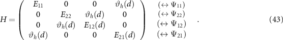
On the diagonal, the exciton energies  (intralayer B excitons) and
  (CT states) enter, where d is the distance and C a constant. These states only couple due to the non-vanishing interaction of the valence bands, denoted as tunneling ϑh
. The corresponding four parameters are extracted from our calculations and the results of the diagonalization of H are given in figure 16(h). Each solution is two-fold degenerate and nicely reproduces the data points from our BSE calculations. At about 2 Å, both curves get energetically closer and an avoided crossing is visible. Due to the latter the intralayer and CT states mix and both peaks are optically active and share the large optical amplitude from the original B transition. It should be noted that similar models have been previously used to describe bilayer TMDCs [121, 122] as well as few-layer systems [123, 124].
(CT states) enter, where d is the distance and C a constant. These states only couple due to the non-vanishing interaction of the valence bands, denoted as tunneling ϑh
. The corresponding four parameters are extracted from our calculations and the results of the diagonalization of H are given in figure 16(h). Each solution is two-fold degenerate and nicely reproduces the data points from our BSE calculations. At about 2 Å, both curves get energetically closer and an avoided crossing is visible. Due to the latter the intralayer and CT states mix and both peaks are optically active and share the large optical amplitude from the original B transition. It should be noted that similar models have been previously used to describe bilayer TMDCs [121, 122] as well as few-layer systems [123, 124].
While the nature of the excitations has been disentangled by the first principles calculations, distance-dependent measurements to verify these predictions are complicated. For instance, pressure would change d to closer distances while also modifying the in-plane properties at the same time. An alternative way to distinguish between intra- and interlayer contributions is to apply a perpendicular electric field. While the physics in one layer remains almost unchanged, the different potential between the layers modifies interlayer properties linearly with the field strength (Stark effect). Figure 17 shows the absorption spectra for different Ez
up to 0.05 eV Å−1. At zero field all peaks are two-fold degenerate due to symmetry. Either intralayer excitons have the same energy in layer 1 and 2, or interlayer states are from layer 1 to 2 and 2 to 1, respectively. For non-zero field strength the A exciton remains almost unchanged. On the other hand, each mixed interlayer exciton splits in two peaks which shift in different directions. The physical reason for these shifts can be understood from the corresponding bands. Both VB and CB of layer 2 are rigidly shifted. Hence, the degeneracy of the transitions  ,
,  is broken, and they change by the potential difference
  , respectively. The inset in figure 17 shows the difference between both peaks. A shift of about 46 meV for 0.05 eV Å−1 is found for the mixed interlayer peaks.
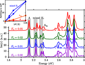
Figure 17. Absorption spectra for a fixed distance  and varying fields Ez
(in eV Å−1). The spectra are vertically shifted for clarity. The inset shows the absolute value of the splittings of the A, mixed IL, and A
and varying fields Ez
(in eV Å−1). The spectra are vertically shifted for clarity. The inset shows the absolute value of the splittings of the A, mixed IL, and A peaks as a function of the field strength. Reprinted with permission from [120]. Copyright (2018) American Chemical Society.
Download figure:
Standard image High-resolution imageIn a joint work with experimental colleagues from Exeter [125], we have been able to demonstrate the expected characteristic field dependence. A schematic sketch of the device is shown in figure 18(a). The bilayer MoS2 is encapsulated by hBN, which is placed between two graphene electrodes. The latter are electrically connected by gold. Panel (b) shows the actual device where each layer is marked. The active part of the device has a large area of about  m [125]. The results of the field-dependent reflectance contrast measurements are summarized in figures 18(c) and (d). For all Ez
a clear peak at the same energy is found slightly above 1.9 eV which is the A exciton. Likewise, a broad B-like excitation is observed. In between an X-shaped peak structure appears. From the zoom in the difference of the gradients of about 0.4 nm can be read, which is the effective interlayer distance perpendicular to the electric field/layers. In theory, we can estimate a similar value. Considering that 35% (65%) are localized on the same (other) layer and the layer distance is 0.6 nm, we find
m [125]. The results of the field-dependent reflectance contrast measurements are summarized in figures 18(c) and (d). For all Ez
a clear peak at the same energy is found slightly above 1.9 eV which is the A exciton. Likewise, a broad B-like excitation is observed. In between an X-shaped peak structure appears. From the zoom in the difference of the gradients of about 0.4 nm can be read, which is the effective interlayer distance perpendicular to the electric field/layers. In theory, we can estimate a similar value. Considering that 35% (65%) are localized on the same (other) layer and the layer distance is 0.6 nm, we find  .
.

Figure 18. (a) Sketch of MoS2 bilayer device encapsulated in hBN with graphene electrodes and an applied electric field Ez . (b) Optical micrograph of the device, the scale bar is 15 µm. The different layers are labeled and indicated by dashed lines. (c) Color plot of the dependence of the reflectance contrast on the electric field for the A, IL, and B at T = 4 K. (d) Stark shifts of the IL feature as a function of Ez extracted from (c). Solid red lines correspond to the linear fits of IL1 and IL2. Reproduced from [125], with permission from Springer Nature.
Download figure:
Standard image High-resolution imageFor a better comparison with our theoretical results, we model the dielectric environment of the device in figure 19. Compared to the previous results in figure 17, we find two main differences: i) The shift of the first peak (IL ) is stronger compared to the second one (B
 ). The reason for the different mixture is the energetic alignment of the initial CT and intralayer B exciton. Due to the additional screening the CT state is lower in energy and the fraction on inter- and intralayer character is no longer symmetric. ii) Furthermore, we find the 2s peak below B
 . As discussed in section 3.3, both the band gap and the exciton binding energy are strongly modified. In contrast to the 1s peak, which is only slightly red-shifted, the distinct energy shift of A
 is another manifestation of the previously discussed effects. Figure 19(b) compares the calculations with the second derivative of the reflectance contrast. Due to the unknown exact device parameters, we have rigidly shifted the energies and scaled the electric fields. Overall a good agreement is found for A and A
 , as well as the IL
 and B
and B . In experiment, the B peak is relatively broad and prohibits an exact comparison.

Figure 19. (a) Calculated absorption spectra of MoS2 bilayer for different perpendicular electric fields Ez . The peak positions are marked by colored dots. the spectra are vertically shifted for clarity. (b) Peak positions of the A (green), mixed IL (red), and B (blue) excitons in comparison with the second derivative of the reflectance contrast measurements. The peak positions from (a) are rigidly shifted to lower energies and the electric field is scaled (due to the unknown dielectric response in the device). Reproduced from [125], with permission from Springer Nature.
Download figure:
Standard image High-resolution imageWhile it may not be surprising that two subsystems have charge transfer states, the appearance in bulk materials has been unexpected. With the same model for the hybridisation as discussed in equation (43), we can expect that mixed IL states will form in multilayer and bulk if intralayer and CT states are close in energy. In particular, the model Hamiltonian (43) is also valid for the bulk (2H phase) with two layers in the unit cell. In several works [81, 126–128] we have investigated the characteristics in bulk MoS2, MoSe2, MoTe2, WS2, and WSe2. While for Mo-based TMDCs interlayer states have been predicted and observed experimentally, the energy alignment (too close to A, small oscillator strength) in W-based materials hinders their detection.
7.2. Heterobilayers
In most homobilayers the energetically lowest state is an intralayer state. The reason for this is that the Coulomb interaction is distance dependent and thus smaller between two layers compared to the layer itself. In the last section we discussed the change of the initial band alignment by an electric field. If two different layers are combined, the bands are typically not aligned due to the different band gaps and work functions. In such a heterobilayer the exciton ground state may be an interlayer transition with a particularly long lifetime.
Prototypical examples are again TMDCs. If we stack two of these layers, the system is no longer commensurate due to the different lattice constants, or can even have rotated lattices. Although these structural differences can lead to many interesting phenomena, we will focus on the properties of commensurable systems which are computationally manageable with our methods. In figure 20, we examine the MoS2/WS2 bilayer. The lattice constant of WS2 is  Å [130] which is only 0.2% smaller compared to MoS
 Å [131]. Here we employ a = 3.160 Å and neglect the small effects due to strain (see section 5). MoS2/WS2 forms a type II bands alignment, i.e. the VBM stems from WS2, while the CBM is located in MoS2. Note that the strongly hybridized bands around
  and halfway between K and Γ may seem to prohibit such a definition. However, for optics we are mainly interested in physics close to K, where the attribution to individual layers is still possible. Thus, the optical properties of the heterobilayer share several similarities with the monolayers. The first strong absorption peaks can be found as A- and B-like excitons. Figure 20(d) shows that both peaks have predominantly intralayer character, i.e. the probability to find the electron and hole in the respective layer is largest. In addition, a tiny peak can be observed about 200 meV below A. From its exciton wave function with hole and electron on different layers, we can clearly identify this as an interlayer state. Although it might be challenging to measure such small oscillator strength in absorption, clear evidence has been found in photoluminescence due to the high occupation [132, 133]. We find an oscillator strength of about 1% compared to the A
 in our calculations. The intensity strongly depends on the distance between the layers in figure 20(e). In a Moiré structure this may suppress the oscillator strength in regions where the atoms are not aligned [134].
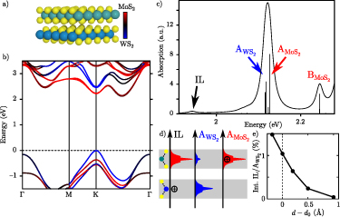
Figure 20. (a) Structure of the lattice-matched heterobilayer of MoS2 and WS2. (b) Band structure of the heterostructure from the GdW approximation. The bands are colored with respect to the character of the monolayer, i.e. red for MoS2, blue for WS2, and black for strong hybridisation. (c) Optical absorption spectrum showing the intralayer excitons (A , A
, A , and B
 ) and the interlayer exciton (IL). (d) Electron probability of the three lowest excitations averaged perpendicular to the heterostructure. (e) Distance dependent ratio of the amplitude of IL and A
 exciton. Reprinted with permission from [129]. Copyright (2018) American Chemical Society.
Download figure:
Standard image High-resolution imageIn addition to the neutral excitons, trions could also be present in the case of a heterobilayer. Figures 21(a) and (b) show a zoom in at low energies for positively and negatively charged trions. The lowest peaks can be found at a trion binding energy of  meV and
  meV, respectively. Interestingly, we find that the nature of this quantum mechanical state can be counterintuitive. Both particles with the same charge can be found on the same layer, i.e. both holes on WS2 or both electrons on MoS2, respectively. The trion with one hole on both layers
  can be found close to the interlayer exciton and appears as its scattering state (which is not fully converged). This assignment is further demonstrated from our ab initio results in figures 21(c) and (d). Although not shown in detail here, the negative T
 further splits in three states (like for the intralayer trions), while T
 remains a single peak. Note that the signature of a trion can generally appear several times in the optical spectra (figure 21(d)). This is a result of detection at
  , where
  can be different final states. For example,
  is responsible for the peak discussed above, and another one is present slightly above the MoS2 exciton (not shown).

Figure 21. Optical absorption spectrum for (a) positively charged trions and (b) negatively charged trions (green) compared to neutral excitons (black) for the energetically lowest states. Sketches of the spatial extent of each state are attached. Besides the exciton X , three different transitions with different character are visible, T
 and
and  are positive trions with two holes on one or two layers, and the negative T
 . c,d) Hole probability of T
 and
and  after averaging over the coordinates of one of the two holes and integrating along both in-plane directions. The electron is fixed on the MoS2 layer. (e) Sketch of the recombination of a trion into two different single-particle states and resulting peaks in the spectrum. Reprinted with permission from [129]. Copyright (2018) American Chemical Society.
Download figure:
Standard image High-resolution imageCalman et al have experimentally measured interlayer trions in MoSe2/WSe2 with a binding energy of 28 meV [135] and thus have validated our prediction.
8. Probing excitations in magnetic fields
In addition to the electric fields discussed in the last section, magnetic fields are frequently employed to probe optical properties [136]. In hydrogen atoms the response to magnetic fields is described by the normal and anomalous Zeeman effect for small fields and the diamagnetic effect for larger fields. Since excitons are conceptually similar to hydrogen, one would also expect their response to magnetic fields to be similar. While effects of a magnetic field on the optical absorption in semiconductors have been measured experimentally and modeled theoretically for various systems in previous decades, a predictive theoretical technique has been missing so far. In [75] we have worked out a first step towards the systematic determination of exciton g factors. Section 2.5 recapitulates the required theoretical framework, which we apply to 2D materials in this section.
We start our investigations for one of the well-known transition metal dichalcogenides namely MoSe2. The calculation of the magnetic moment  in a periodic system is given by equation (39). Before we evaluate this, we take a look at the local limit
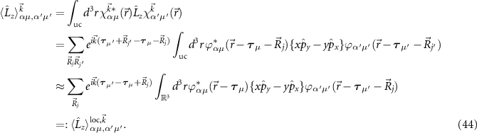
Here  are the lattice periodic basis functions which lead to a double sum over the lattice vectors and an integral over the unit cell. Because x and y appear in addition to the two localized functions, the common transformation to the relative distance (used for other matrix elements) is no longer valid. To check the importance of the double sum, we calculate
  and thus
  , which is plotted in figure 22. In panel (a), all values
  are between ±2
  which is consistent with
  for
for  (s, p, and d electrons). In the topmost valence bands and lowest conduction band close to K point, we find a value of
  for both spin-orbit split bands and
  for the conduction bands. These values can be understood by the character of the wave functions and the spherical harmonics. The VBM has contributions of 80% of Mo d orbitals with
  character (
 and dxy
orbitals) and 18% of
and dxy
orbitals) and 18% of  orbitals of Se. Close to the CBM, the contribution of Mo
  (
( orbital) is about 55% and the magnetic moment is much closer to zero.
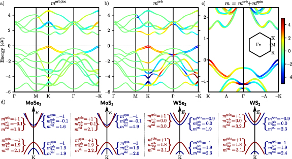
Figure 22. DFT band structure of MoSe2 with bands colored according to (a) the expectation values of the local orbital magnetic moments  , (b) the orbital magnetic moment
  , and (c) zoom in for the total magnetic moments
  . (d) The different contributions of the magnetic moments mspin,
  , and
, and  for different TMDC materials. For each band at the K point the values are given in units of
  . The sketched bands are colored according to the spin character. Reprinted figure with permission from [75], Copyright (2020) by the American Physical Society.
Download figure:
Standard image High-resolution imageGoing beyond the local approximation [68, 69], figure 22(b) shows several important quantitative differences. While  remains zero along
  –M, clearly different values are found in the rest or the Brillouin zone. In the VB the values are close to 4, while those in the CB are slightly smaller than
  . The difference
  is 2.1 and
  , respectively. The spin contributions are still missing for the total moments; the sum of both in plotted in figure 22(c). Due to the different spin character both valence and both conduction bands get different contributions. The resulting values at K are compared in panel (d). While
  and mspin are almost similar in all four TMDCs (besides the changed band characters in Mo- and W-based materials), the contributions due to the Bloch character mval are different. It is different both in between the bands in one material and between Mo- and W-based compounds.
The final step to calculate the optical response is to use the weights of the corresponding excitations in equation (40). To this end, we solve the Bethe–Salpeter equation to find the exciton weights on a mesh on  points, similar to what we have previously discussed for MoS2 in figure 4. Figure 23 shows the differences of the magnetic moments of the CB and the VB, and CB+1, respectively. Panels (a) and (b) are MoSe2, (c) and (d) show WS2. Due to the different ordering of the spin character in both materials, the values close to ±K are
  for the CB in MoSe2 but for the CB+1 in WS2. The contributions of the dark (spin-forbidden) state are about two time larger. The much smoother character for WS2 stems from the missing band crossings in contrast to Mo-based materials.

Figure 23. (a), (b) Difference of the magnetic moments of MoSe2's first and second conduction band (CB, CB+1), respectively, and the VB. The results (in units of  ) are plotted on a
  mesh, with colors from red to blue denoting the differences. (c), (d) Same for WS2. Note that the abrupt changes (e.g. red to blue) are related to band crossings. Reprinted figure with permission from [75], Copyright (2020) by the American Physical Society.
Download figure:
Standard image High-resolution imageThe exact values are listed in table 1. Besides the magnetic moments at K and their differences gband (equation (41)), we list the g factors of the A and B excitons evaluated with equation (40). We find that g is more than 30% smaller compared to gband due to the spatial structure of the excitons. For instance, for MoSe2 the interband transition exactly at K changes by the magnetic moment of  (reversed at −K), and thus
  . Away from ±K the absolute value of the magnetic moment decreases and thus gA is only −3.2. Overall, the theoretical and experimental g factors agree well (table 1), even if an exact comparison is difficult due to the varying experimental values. The g factor of the dark exciton is reduced from
  to
to  respecting the excitonic nature. In addition to momentum direct excitons discussed previously, we can also use equation (40) to evaluate indirect excitons [86]. For example, we find g = 12.0 (
 ) for the lowest energy transitions for K→K' and
  (
( ) for K
 .
.
Table 1. Magnetic moments from equation (39) (in  ) at the K point, their differences
  which resemble the main contribution of the bright A and B transitions (e.g., for MoS
 and
and  ), and the resulting g factors from equation (40). For comparison, several experimental measurements of the g factor of the A and B exciton are listed. Note that we expect an error of about
  for our magnetic moments m and about ±0.1 for the g factors.
| Material |

|

|

|

| Exp. gA |
|---|---|---|---|---|---|
| MoS2 | 2.94/5.10 | 2.98/0.76 | −4.24/−4.36 | −3.06/−3.10 | −1.7 [137], −3.0 [138], −3.8 [138], −4.0 [76], −4.2 [139], −4.6 [140] |
| MoSe2 | 2.81/5.03 | 2.74/0.46 | −4.58/−4.70 | −3.22/−3.28 | −3.8 [141, 142], −4.1 [143], −4.2 [139], −4.3 [138], −4.4 [140] |
| MoTe2 | 2.71/5.03 | 2.60/0.21 | −4.86/−5.00 | −3.36/−3.36 | −4.6 [138, 144] |
| WS2 | 3.29/5.94 | 1.35/4.21 | −3.46/−3.88 | −2.76/−2.80 | −3.7 [139], −3.94 [76], −4.0 [138], −4.25 [145], −4.35 [146] |
| WSe2 | 3.15/5.91 | 0.99/3.97 | −3.88/−4.32 | −3.00/−3.22 |
 [147], −3.2 [148], −3.7 [142], −3.8 [139], −4.37 [149] [147], −3.2 [148], −3.7 [142], −3.8 [139], −4.37 [149] |
9. High-throughput exploration of hypothetical two-dimensional materials
Two-dimensional materials have emerged as a new class of materials in the last decade. In the last sections we have mostly discussed the properties of transition metal dichalcogenides and black phosphorus. However, since the observation of graphene [7] more than fifty monolayer compounds have been synthesised or exfoliated [3]. This asks for a more systematic study of stable 2D materials and their properties. In this section we will discuss a set of more than 4000 materials which we have studied and stored in the 'Computational 2D Materials Database (C2DB)'. To be able to compute such a large set of materials, a well-defined and automated workflow is essential. This high-throughput approach is implemented in python scripts employing the ASE and GPAW code [59, 60].
In this large set of materials, we find a great variability of properties published in [3, 38, 150, 151]. For instance, several TMDC show an anisotropy like ReSe2 [152], several materials have a magnetic ground state like CrI3 (which we have analysed in detail in the heterobilayer with WSe2 [40]), or they belong to the class of Janus materials, i.e. compounds with different top and bottom layers, that have a built-in dipole moment. Further high-throughput studies suggest many more new materials [153].
After a short discussion of the workflow with special attention to GW calculations, we investigate the Janus material MoSSe in more detail. Many further results are accessible through the website https://cmrdb.fysik.dtu.dk/c2db.
9.1. Structure workflow
As for conventional 3D materials, the number of hypothetical 2D materials is essentially unlimited. Thus, it is important to select reasonable candidates and start with a good guess of their lattice and atomic structure. The most important classification scheme is the symmetry. Figure 24(a) shows the five different 2D Bravais lattices. Together with the basis, this defines different materials. Some examples are shown in figure 24(b), e.g. graphene [7], MoS2 [10], WTe2 [154], CrI3 [155], TiS3 [156], FeSe [157], or FeOCl. For our screening study, we use already known 2D materials as prototypes and substitute their atoms by chemically similar ones. For example, we replace carbon with silicon, germanium, tin, etc in graphene, or molybdenum with other transition metals and sulfur with other chalcogenides in MoS2. Due to this structure generation strategy, most of the candidates are quite simple, i.e. they are binary or ternary compounds, and the number of atoms in the unit cell is limited to a small number.

Figure 24. (a) The five possible Bravais lattices in two dimensions. The red dots show repetitions of the lattice vectors  and
and  (enclosing the angle γ). The grew area denotes the smallest possible unit cell. (b) Some example materials with different structures and compositions. The top panel is a top view, the bottom panel is a side view. While C, MoS2, and CrI3 have a hexagonal symmetry, the other examples are rectangular. Reproduced from [3]. © IOP Publishing Ltd. All rights reserved.
Download figure:
Standard image High-resolution imageWith these structural guesses, we begin our structure workflow, which is shown in figure 25. After an initial relaxation which preserves the symmetry, we check that the system is still one two-dimensional layer and that it is not already included in the C2DB. If it is, we continue with the classification including its magnetic state. To check the stability, three different criteria are evaluated: 1) The formation energy needs to be less than zero which means that the total energy of the atoms reduces (relative to the standard states of the constituent elements) due to the interaction with other atoms. If this is not case, a small perturbation or even a temperature larger than 0 K would be sufficient to degenerate the material. We also compare the total energy to those of other phases, e.g. for graphene we compare to diamond etc. If the energy of the current 2D configuration is much higher, it is most probably unstable. 2) We evaluate the stiffness tensor and its eigenvalues. If any of them is negative, this is a clear sign that the structural relaxation has not found a minimum on the energy surface. 3) The dynamic matrix is set up at the high-symmetry points of the  supercell, and we calculate its eigenvalues. If an eigenvalue is below zero, this indicates that the system would further relax in a larger cell and is therefore unstable in the current configuration. If the material is unstable, we store this result in the database and do not consider the material further. If, on the other hand, the material is stable, we continue to investigate its properties in more detail. Materials of particular interest for opto-electronics are transition metal dichalcogenides for which we find about 70 candidates with different compositions that are stable (see MoS2 and WTe2 in figure 24).

Figure 25. The structure workflow: starting from an initial guess, the relaxed structure is analysed and the stability is checked (see main text). Depending on the result, the candidate is stored in the database with or without further properties. Reproduced from [150]. © IOP Publishing Ltd. All rights reserved.
Download figure:
Standard image High-resolution image9.2. Properties and statistics
Once the structure has been determined, we are able to evaluate a large set of properties automatically by our ab initio property workflow, which includes Bader charges, Born charges, out-of-plane dipoles, work functions, exchange couplings, magnetic anisotropies, deformation potentials, plasma frequencies, piezoelectric tensors, spontaneous polarizations, band structures (within different approximations) and density of states, effective masses, Fermi surfaces, topological invariants, infrared polarizabilities, optical polarizabilities, optical absorbances, Raman spectra, and second harmonic generation. For a more detailed discussion of all these properties, we refer to [3, 150] in the appendix. Here we briefly discuss the statistics of band gaps and band positions. Figure 26 shows the resulting band gaps for more than 250 semiconducting materials for which we used different approximations: PBE [25] is a widely used generalised gradient approximation, HSE [27] replaces 25% of the local exchange by the non-local exchange potential for the short-range part of the Coulomb interaction, and GLLBSC [158] is an approximation to the optimised effective exchange potential that includes an estimate of the derivative discontinuity for the band gap. The band gaps obtained with these approximations are plotted in blue, orange, and green with respect to the  results. The left panel shows the band gaps and indicates that PBE and HSE clearly underestimate the
  values on average by about 45% and 22% in 2D materials. GLLBSC provides a much better estimate for the band gap, but the position with respect to vacuum (right panel) and distances to other bands (not shown here) are problematic. On the other hand, the predicted band positions in PBE and HSE clearly follow the trends of the
  results. While we perform
  and BSE calculations for semiconductors with less than six atoms per unit cell, all other properties are calculated using the PBE functional.
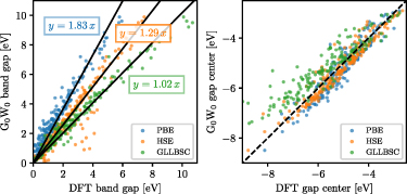
Figure 26. Band gaps and gap centers (average of VBM and CBM) of more than 250 materials calculated with PBE, HSE, and GLLBSC (blue, yellow, and green dots). Reproduced from [3]. © IOP Publishing Ltd. All rights reserved.
Download figure:
Standard image High-resolution image9.3. Automated GW calculations
While DFT has become a standard method and is relatively easy to use, MBPT is much more involved. This is due to several parameters which have to be converged simultaneously, such as the additional basis representing the two-point functions, or the  integral (over the first Brillouin zone) and the energy dependence of the self-energy. Moreover, MBPT in the GW approximation scales an order of magnitude slower, i.e.
  where N is the number of electrons (compared to
  in DFT), and the prefactor is much larger. Depending on the exact implementation, this only allows for small systems of a few dozen of atoms or less. Therefore, high-throughput calculations are particularly challenging [38].
As a first step towards fully automated GW calculations, we have analysed a set of 370 GW calculations for 2D materials to establish the validity and limitations of various commonly used approximations and extrapolation schemes [38]. As an example, we briefly mention one aspect pertaining to the renormalization factor Z. The left panel of figure 27 shows the GW band structure of monolayer MoS2. While most points are reasonable, the third conduction band at K shows a drastic and unphysical jump. This can be traced back to the moderately converged derivative of the self-energy (equation (13)), which enters by the quasi-particle weights  . This behavior is observed for other materials as well. In general such cases can be identified by the condition
 ![$Z \not\in [0.5, 1.0]$](https://content.cld.iop.org/journals/2516-1075/5/3/033002/revision2/estace86cieqn267.gif) , which indicates either a numerical/convergence issue or a break down of the quasi-particle approximation. We refer to such states as quasi-particle inconsistent states. While for a single material more rigorous convergence can be helpful, this is impractical in a database. Another possibility is to set Z to the average value 0.75. In the right panel of figure 27 the resulting changes of the quasi-particle shift are shown. While the distribution is slightly broader, the absence of outliers reduces the mean absolute error to 0.09 eV. An even better result can be obtained if Z = 0.75 is used only when
, which indicates either a numerical/convergence issue or a break down of the quasi-particle approximation. We refer to such states as quasi-particle inconsistent states. While for a single material more rigorous convergence can be helpful, this is impractical in a database. Another possibility is to set Z to the average value 0.75. In the right panel of figure 27 the resulting changes of the quasi-particle shift are shown. While the distribution is slightly broader, the absence of outliers reduces the mean absolute error to 0.09 eV. An even better result can be obtained if Z = 0.75 is used only when ![$Z \not\in [0.5, 1.0]$](https://content.cld.iop.org/journals/2516-1075/5/3/033002/revision2/estace86cieqn268.gif) (MAE becomes 0.06 eV, not shown here).
(MAE becomes 0.06 eV, not shown here).
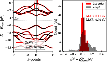
Figure 27. The left panel shows the band structure of monolayer MoS2 (red) and after replacing unrealistic Z with 0.75 (empZ, black). The right panel shows the distribution of QP shifts with first-order Newton–Raphson compared to empZ. Reproduced from [38]. CC BY 4.0.
Download figure:
Standard image High-resolution image9.4. Janus MoSSe
A novel class of 2D materials that we have investigated are the so-called Janus monolayers. These are materials, for instance TMDCs, in which the atoms at the top and bottom of the monolayer are not identical such that the out-of-plane mirror symmetry is broken. Lu et al [159] have fabricated and measured MoSSe in 2017. Its structure (see figure 28(a)) is similar to that of the TMDCs discussed previously. The lattice constant of 3.241 Å is in between those of MoS2 and MoSe2 (3.16 and 3.30 Å). Due to the different work functions above and below the layer, the potential differs by 0.75 eV, so the material has a build-in dipole.

Figure 28. (a) Averaged potential  perpendicular to the MoSSe layer. The work function differs by 0.75 eV on both sides. (b) Band structure in the LDA (grey dashed) and the GdW(LDA) approximation (black). The band gap is 2.64 eV, and the VBM are set to zero. Note that the spin-orbit-split CBs close to K do not cross. (c) Optical absorption spectrum of MoSSe. The main peaks are labeled. The energetically lowest bright peak A is at 1.88 eV, and the first (dark) excitation is 25 meV below. Reprinted with permission from [151]. Copyright (2019) American Chemical Society.
Download figure:
Standard image High-resolution image
The band structure in figure 28(b) shows the typical direct gap at the K point. The gap of 2.64 eV is (again) in between those of 2.89 eV for MoS2 and 2.57 eV for MoSe2. This is also true for the spin-orbit splittings of the VBs and the CBs (210 meV and 30 meV), compared to MoS2 (180 meV and 15 meV) and MoSe2 (230 meV and 42 meV). Similarly, the lowest CB has opposite spin polarization compared to the highest VB. But unlike MoS2 and MoSe2, we do not find that the CBs cross. Instead, the character changes due to an avoided crossing.
The optical absorption shows a similar trend (figure 28(c)). Two clear excitons A and B originate from direct transition between the spin-orbit-split bands. In addition, excited states (2s, etc) and a broad peak structure C (originating from transitions in different parts in the Brillouin zone) reside below the band gap. The first bright exciton can be found at 1.88 eV, and the first dark exciton is about 25 meV lower in energy. Compared to previous results (25 meV in MoS2) [82], we expect that the lowest excitation is dark in MoSSe similar to MoS2. MoSSe is only one possible candidate. Employing tellurium or changing the transition metal (to tungsten or similar) suggests many further interesting Janus materials. E.g. we found semiconducting materials with direct and indirect band gaps ranging from 0.7 eV for CrSTe to 3.0 eV for BiClS. These have finite out-of-plane dipoles with a difference of the vacuum level up to 1.5 eV as well as large Rashba-splittings up to 75 meV.
10. Conclusions and outlook
In this review we summarize several investigations of the electronic and optical properties of 2D semiconductors which are obtained by employing and extending ab initio techniques. We examine several 2D materials and ways to design the optical excitation in them. In addition to exploring the excitations in the intrinsic, freestanding monolayer, we find potentially strong modification by the substrate on which the material is placed, by free carrier doping which leads to three-particle states, or by structural deformations when applying strain. In addition, defects and adsorbates can strongly alter the excitation spectrum, as well as the stacking of different 2D materials, which allows for excitations between the sub-systems, most notably interlayer excitons and trions. Furthermore, electric and magnetic fields can be applied to study and tune the response of the optical properties. The main computational methods applied are the DFT, the many-body perturbation theory in the GW and GdW approximation, and the Bethe–Salpeter equation which are extended by complementary developments, e.g. to capture the three-particle effects or the magnetic response of excitons.
The emphasis of the results presented is on the comparison to experiments. Due to the large number of measurements for the transition metal dichalcogenides, we have often focused one of the five materials MoS2, MoSe2, MoTe2, WS2, or WSe2 in our calculations. For several effects like substrates, momentum dependent excitons, or the magnetic response our results provide new fundamental insight. For other topics such as excited state trions, interlayer excitons, or interlayer trions, our predictions have been verified by corresponding experiments. Many of the results obtained for the TMDCs are of general nature, i.e. related to the 2D nature rather the specifics of materials, and are thus expected to carry over to other 2D semiconductors.
The described methods in this review and their combination can also provide helpful ways for experimental studies of further physical effects. For example, the usage of electric fields is predestined to distinguish intra- and interlayer excitations. Doping or magnetic fields can provide further insights into the character of the involved quantum mechanical states.
In the last section, we have presented a few results from high-throughput studies of thousands of 2D materials. Besides the opto-electronic properties, a couple of systems have interesting topological [160] or magnetic properties [40]. For instance several materials show out-of-plane magnetization (like CrI3), while other are polarized in-plane (and couple antiferromagnetically to the neighboring layers, like CrSBr [161]). In particular, the possibility to stack these layers promises novel physical phenomena and applications.
From a methodological point of view, ab-initio techniques are well-established for the investigation of opto-electronic properties. But there are still many open questions that need to be addressed. For instance, the introduced methodology to calculate trions can (in principle) be straightforwardly extended to evaluate four- or five-particle complexes, etc which have been reported in the literature [162, 163]. To gain deeper insights into the lifetimes and dynamic processes of excited states, the coupling of electronic and vibronic degrees of freedom and the consideration of the temperature is essential [164–166]. Their careful treatment is a difficult task which is still beyond state-of-the-art.
Acknowledgment
We thank P Krüger for fruitful discussions. T D gratefully acknowledges the Gauss Centre for Supercomputing e.V. (www.gauss-centre.eu) for funding this project by providing computing time through the John von Neumann Institute for Computing (NIC) on the GCS Supercomputer JUWELS [167] at Jülich Supercomputing Centre (JSC) and the financial support from the Deutsche Forschungsgemeinschaft (DFG, German Research Foundation) through Project No. 426726249 (DE 2749/2-1 and DE 2749/2-2). M R acknowledges support from the DFG Collaborative Research Center SFB 1083 (Project No. A13). K S T acknowledges funding from the European Research Council (ERC) under the European Union's Horizon 2020 research and innovation program Grant No. 773122 (LIMA) and the Villum Investigator Grant No. 37789 supported by VILLUM FONDEN.
Data availability statement
The data cannot be made publicly available upon publication because they are not available in a format that is sufficiently accessible or reusable by other researchers. The data that support the findings of this study are available upon reasonable request from the authors.