

Abstract
This review outlines fundamental principles, instrumentation, and capabilities of angle-resolved photoemission spectroscopy (ARPES) and microscopy. We will present how high-resolution ARPES enables to investigate fine structures of electronic band dispersions, Fermi surfaces, gap structures, and many-body interactions, and how angle-resolved photoemission microscopy (spatially-resolved ARPES) utilizing micro/nano-focused light allows to extract spatially localized electronic information at small dimensions. This work is focused on specific results obtained by the author from strongly correlated copper and ruthenium oxides, to help readers to understand consistently how these techniques can provide essential electronic information of materials, which can, in principle, apply to a wide variety of systems.
Export citation and abstract BibTeX RIS

Original content from this work may be used under the terms of the Creative Commons Attribution 4.0 licence. Any further distribution of this work must maintain attribution to the author(s) and the title of the work, journal citation and DOI.
1. Introduction
In recent years, angle-resolved photoemission spectroscopy (ARPES) has been widely recognized as one of the leading experimental probes in the research field of condensed matter physics. This stems from its spectroscopic capability as it can directly measure microscopic electronic states that are deeply related to macroscopic physical phenomena. Therefore, developments on ARPES-techniques/instruments have been holding a crucial key to accelerate progress in modern condensed-matter physics. For instance, at the dawn of the ARPES technique, considerable efforts have been devoted to improving its energy and momentum resolution pushed by a desire to capture fine electronic structures of high-Tc superconductors. This movement established high-resolution ARPES measurement (implying high energy and momentum resolution), which resulted in various key experimental findings for the understanding of high-Tc cuprate physics, such as the large Fermi surface topology, d-wave superconducting gap, normal-state pseudogap, kink in the electronic dispersion, and so on [1, 2]. In particular, high energy and momentum resolution extended the unique capabilities of ARPES, allowing us to access interaction effects or electronic self-energies that dominate the physical properties of correlated electron systems [3, 4]. Subsequently, different types of ARPES technique have been developed and leading pioneering research by integrating a new function: a spin resolution to study magnetic properties by examing spin-polarized electronic states (spin-resolved ARPES) [5, 6], a temporal resolution to track an ultrafast dynamics by pump–probe type experiment (time-resolved ARPES) [7], and a spatial resolution to pursue a local electronic state by utilizing a micro- or nano-spot beam (spatially-resolved ARPES) [8, 9]. These advanced ARPES techniques have successfully applied not limited to the correlated electron systems but also a wide variety of materials, especially, topological quantum materials these days, for the understanding of their physical properties and behaviors in terms of the electronic and spin structures [6, 10, 11].
Among these developments, this review aims to deliver rich capabilities of high-resolution ARPES technique, becoming a rather standard characterization tool, and to introduce spatially-resolved ARPES, which could be a future-standard technique among the state-of-the-art ARES techniques. We start with the elementary discussions on principles and tips of ARPES methodology and instrumentation in section 2. The broad overview of the high-resolution ARPES and spatially-resolved ARPES techniques are given in sections 3 and 4, respectively. We also present those analysis methods and specific results obtained from ruthenate and cuprate superconductors by the author. Finally, we conclude the paper with future perspectives in section 5.
2. Methodology and instrumentation
2.1. Methodology
The photoemission intensity is widely interpreted following the so-called three-step model, which is a conceptually much simpler model compared with the rigorous one-step model [2]. Based on the three-step model, ARPES intensity can be written as functions of energy ω and momentum k of the electrons as

except for extrinsic backgrounds  and instrumental broadenings
  . The first term
  is proportional to the square of the dipole matrix element,
  . Here, the
  represents a transition from one-electron initial states
  to final states
  due to the photon perturbation with a vector potential
A
, interacting with the electron specified by a momentum operator
p
. The second term
due to the photon perturbation with a vector potential
A
, interacting with the electron specified by a momentum operator
p
. The second term  is the single-particle spectral function, and contains the information of electronic band structures and lifetimes, written as

Here,  is the non-interacting (bare) energy-band dispersion, and the complex electron self-energy
  is introduced to express the energy and lifetime of a dressed electron (quasiparticle) as
  and
and  , respectively. The third term
  is the Fermi–Dirac function,
  , so that only occupied states are observable by ARPES though the unoccupied states can be slightly accessible within a range of thermal broadening ∼4kB
T. As shown in equations (1) and (2), one can thus evaluate the electron self-energy by analyzing ARPES spectra. However, the measured intensity is not directly corresponding to a raw spectral function but weighted by the matrix element, which depends on energy and polarization of the incident light as well as experimental geometry. Thus, these experimental factors are essential to interpret the ARPES spectra, as discussed below.
, so that only occupied states are observable by ARPES though the unoccupied states can be slightly accessible within a range of thermal broadening ∼4kB
T. As shown in equations (1) and (2), one can thus evaluate the electron self-energy by analyzing ARPES spectra. However, the measured intensity is not directly corresponding to a raw spectral function but weighted by the matrix element, which depends on energy and polarization of the incident light as well as experimental geometry. Thus, these experimental factors are essential to interpret the ARPES spectra, as discussed below.
2.2. Instrumentation
The experimental configuration of ARPES is schematically drawn in figure 1(a), where core components, incident light, electron analyzer, and sample, are highlighted. As we will see below, these components are closely related to flexibility as well as the resolution in ARPES experiments. Hence, those utilizations and improvements are deeply connected with the development/sophistication of the ARPES technique.

Figure 1. (a) Schematics of ARPES measurement with relevant experimental factors. (b) and (c) Energy and momentum conservation rules in the photoemission process, respectively [12].
Download figure:
Standard image High-resolution image2.2.1. Incident light source
Synchrotron radiation or laboratory light sources (gas-discharge lamp or laser light source) are used as the incident light for ARPES experiments. As summarized in table 1, the two types of sources have different specifications and thus complement each other. The synchrotron radiation has a significant advantage in delivering tunable photon energy from vacuum ultraviolet (VUV) to soft x-ray (SX) range (∼5 eV to 1 keV) continuously depending on the beamline design. Various types of modern ARPES beamlines have been developed in the world [12–17]. Some new/commissioning beamlines can provide a vast energy range [e.g. 21-ID-1 beamline (20–2000 eV) at National Synchrotron Light Source II (USA) [18], Dreamline (20–2000 eV) at the Shanghai Synchrotron Radiation Facility (China), LOREA beamline (10–1000 eV) at the ALBA (Spain), and Bloch beamline (10–1000 eV) at the MAX IV (Sweden)]. In contrast, the laboratory light sources have the advantage of achieving ultimate energy resolution (∼1 meV order). Although they can basically generate a single photon-energy due to the laser [19–22] or gas emissions [23–25], its variation and tunability have been increased for high-resolution ARPES experiments by utilizing the high-harmonic generation (HHG) [26–30] as well as the various kinds of rare gas (Xe, Kr, Ar, and He) [25, 31, 32]. Note that wide variety of HHG sources has been growingly developed for time-resolved ARPES experiments that providing higher excitation energy, while the energy resolution has to be relaxed to achieve high temporal resolution due to the energy-time uncertainty principle as described in the next subsection 2.2.2: 22.1 eV (170 meV, 11 fs) [33], 22.3 eV (100 meV, 65 fs) [34], 21.7 eV (110 meV, 40 fs) [35]. In contrast, by relaxing the temporal resolution, various time-resolved ARPES systems have been also developed to be compatible with high energy resolution: higher excitation energy with high energy resolution and moderate temporal resolution: 11 eV (16 meV, 250 fs) [36], 21.8 eV (21.5 meV, 320 fs) [37], low excitation energy but with very high energy resolution and moderate temporal resolution: 5.9 eV (10.5 meV, 240 fs) [38], 5.9 eV (11.3 meV, 310 fs) [39], 6.3 eV (9 meV, 700 fs) [40], and furthermore, widely variable excitation energies with high energy resolution and moderate temporal resolution: 24–33 eV (30 meV, 200 fs) [41], 8–40 eV (22 meV, 190 fs) [42], 17–31 eV (22 meV, 105 fs) [43].
Table 1. Typical specifications of representative light sources for high-resolution ARPES experiments. The HHG laser sources for pump–probe time-resolved ARPES experiments are listed in the text.
| Laboratory | |||
|---|---|---|---|
| Light source | Synchrotron | Laser | Gas-discharge lamp |
| Photon energy (hν) | 5 eV–1 keV [13, 14] | 6 eV [19, 22], 7 eV [20, | 5–7 eV (Xe) [32], 8.4 eV (Xe) [25], |
| 21], 5.9–6.4 eV [29], 5.3–7 eV [150], | 8.4, 10.0, 11.8 eV (Xe, Kr, Ar) [31], | ||
| 10.5 eV [26], 10.7 eV [28], | 21.2 eV (He I) [23], | ||
| 11 eV [27, 30] | 40.8 eV (He II) [24] | ||
| hν tunability | Tunable | Little | Untunable |
| Polarization | Variable | Variable | Non-polarized |
| k-space coverage | Multiple BZ | lesssim 1.0, 1.7 BZ | lesssim 1.0, 1.8, 2.7 BZ |
| Photon flux | 1012 photons/s | 1013–1015 photons/s | 1012 photons/s |
| Spot size | ∼0.1 mm | ∼0.1 mm | ∼1 mm |
The tunability of the photon-energy over the broad energy region plays a critical role in ARPES experiments in several viewpoints as follows: (1) matrix element effects, (2) accessible momentum region, (3) surface/bulk sensitivity, and (4) energy and momentum resolutions. As will be explained below, the choice of photon energy is linked with various aspects in the ARPES experiments, and hence, it must be carefully done to satisfy experimental demands.
(1) Matrix element effects: it is essential to examine the matrix element effects by varying photon energies as well as polarizations to extract intrinsic information on a raw spectra function from ARPES spectra, as seen in equation (1). Similarly, the photon-energy varies the photoionization cross-section [44], which appears differently depending on an orbital character. In other words, tunable photons can provide orbital selectivity. Besides, it should be noted that the utilization of the linear polarization of the light can give the selectivity of the orbital symmetry [2], as we will demonstrate in section 3.
(2) Accessible momentum region: the available energy range is also related to an accessible parallel momentum ( ). As shown in figures 1(b) and (c), the energy and parallel momentum conservation rules hold in the photoemission process:


Here, hν is the energy of the incident photon where h is the Plank constant and ν is the frequency of the light, Ekin is the kinetic energy of photoelectrons, EB is the binding energy of electrons, ϕ is the work function (typically 4–5 eV for metals) required for the electron to escape from the solid through the surface and to reach the vacuum level Evac, and ℏ is the reduced Plank constant given by h/2π. As seen in equation (4), for the given kinetic energy Ekin and emission angle θ of photoelectrons, the accessible parallel momentum is then given by  where one can also replace
  by the Fermi energy EF = hν − ϕ. Therefore, in the case of low-energy photons, one needs to pay attention to the fact that the detectable k-space can be less than the first Brillouin zone (BZ) (ex.
  for hν ∼ 6 eV and in-plane lattice constant ∼4 Å). Similarly, the tunable photon-energy is also required to survey the three-dimensional BZ as the perpendicular momentum k⊥ is given by

where the V0 is an unknown and material-dependent parameter called an inner potential, which can be experimentally determined via the periodicity of the band structure seen in the photon-energy dependent measurements.
(3) Surface/bulk sensitivity: it is well-known that inelastic mean free path λIMFP depends on the electron kinetic energy, and its dependence is often called as a universal curve [45]. Hence, surface/bulk sensitivity is varied with the photon-energy: the λIMFP is shortest less than 5 Å in the VUV region, while it becomes ten-times longer in the SX (∼1 keV) and low-energy (<10 eV) regions. However, in the low-energy region, the bulk sensitivity is not always enhanced due to strong final-state effects. Thus, the SX–ARPES is most often used to study interface or bulk states by utilizing its better bulk sensitivity [46].
(4) Energy and momentum resolution: a lower photon energy can provide a better energy resolution because the total energy resolution can be written as ΔEtot = E/Rsys, where Rsys is a resolving power (E/ΔEtot) of a whole system. On the other hand, both in-plane and out-of-plane momentum resolution also depends on the photon-energy. While the in-plane momentum resolution becomes better for lower photon-energy following

for a given angular resolution Δθ in case of hemispherical electron analyzer, the out-of-plane resolution can be improved for the longer λIMFP due to the Heisenberg uncertainty principle because

In other words, in-plane electronic dispersions on the sample surface can be better resolved at lower photon-energies, though out-of-plane dispersions along k⊥ are well resolved for the longer λIMFP by using higher photon-energies in the SX region.
2.2.2. Electron analyzer
To achieve high energy-resolution in ARPES experiments, one needs to take into account components of the total energy resolution ΔEtot as given by

where the ΔEhν includes a bandwidth of the incident light as well as the contributions from the optics for generating/delivering the light, and the ΔEana is determined by the resolving power of the electron analyzer. If ΔEtot is beyond this estimation, extrinsic contributions are suspected, most likely due to electric noises originated from insufficient sample grounding or electrical instability of power supply. However, it can usually be negligible in a properly designed system. Focusing on the first term in equation (8), the laser or gas-discharge lamp has been considered most suitable for achieving ultimate resolution because of their natural narrow linewidth less than one meV. However, modern synchrotron beamline can also deliver high-flux radiation with a high resolving power of hν/ΔEhν ∼ 20 000 (i.e., ΔEhν = 1 meV for hν = 20 eV) despite that the synchrotron radiation needs monochromatization by a diffraction grating. On the other hand, the pulsed nature of the light should also be carefully considered because of the space charge effects, which cause energy shift and broadening due to Coulomb repulsion in a dense electron cloud if too many photoelectrons are excited in a short time and from a narrow area [47–52]. In this regard, a high repetition rate is necessary to avoid space charge effects by reducing photons per pulse. Besides, a long pulse duration (ex. Δt = 1 ps for ΔEhν = 660 μeV) is required from the viewpoint of the time-energy uncertainty relation (ΔEhν ⋅ Δt ⩾ ℏ/2). This trade-off relationship between energy and temporal resolutions becomes especially crucial in time-resolved ARPES experiments. Also, it was reported that the mirror image potential effects compensate for the space charge effects in such long pulse duration (1–10 ps) [47]. Then, the energy resolution of the electron analyzer in the second term in equation (8), can be given by

where EP is the electron pass energy, w and R is the slit width and radius of the hemispherical electron analyzer, respectively, and α is the half-angle of the angular spread of the photoelectrons at the entrance slit [53]. Here, the contribution from the second term EP α2/4 is often omitted to a first-order approximation, because the angular spread α becomes reasonably small (<1°) even for a moderate-size spot (<1 mm) when the system is well aligned, that is, the plane of emission (or incidence) is parallel to the detection plane of the analyzer. Therefore, one can expect ΔEana ∼ 1 meV for EP = 2 eV and w = 0.2 mm by using a modern electron analyzer with R = 200 mm. On the other hand, momentum-resolution Δk// depends on two parameters, as seen in equation (6): the kinetic energy of photoelectrons Ekin and angular resolution of the electron analyzer Δθana. The former can be significantly reduced for low-energy photons, making low-energy ARPES be a unique tool providing a superior momentum resolution [54–57]. The latter can be described by

meaning that the photoelectrons emitted from the same emission angle will have a lateral spread. In other words, the beam spot Δdhν is magnified on the detector with a certain factor M, which is determined by the lens mode and the retardation ratio. Then, the angular dispersion of the lens mode D transforms the spread value on the detector into the angular unit. As is apparent, a smaller spot size provides a better angular resolution, indicating the positive correlation between the spatial and angular resolutions, as practically demonstrated in section 4.1. On the contrary, one should also consider the uncertainty relation between the position and momentum, Δx ⋅ Δk ⩾ 1/2, representing the negative correlation between these resolutions. Compared with a typical momentum resolution in modern ARPES instruments (10−3–10−4 Å−1), the momentum uncertainty has virtually no effect (10−5 Å−1) in the case of a microbeam. However, it becomes non-negligible (10−2–10−3 Å−1) for a nano-focused beam (1–10 nm).
Besides the resolution aspect mentioned above, the detector of the analyzer is also a vital factor in ARPES. For instance, the development of the hemispherical electron analyzer with a multichannel plate enabled capturing a snapshot of two-dimensional photoemission signals, that is, the photoemission signals I(Ek ) with different emission angles along the detector slit (θx ) can be measured simultaneously, providing I(Ek , kx ) within a certain acceptance angle of the detector. It significantly improved not only the efficiency but also data visualization of ARPES, which greatly helps to recognize electronic features (ex. those induced by many-body interactions). Furthermore, recently developed deflector-type electron analyzer enabled measuring the two-dimensional angular distribution (θx , θy ) by deflecting the electron trajectories, providing I(Ek , kx , ky ) within a certain acceptance and deflection angle of the detector. One of the most advantages of the deflector-type analyzer is that it does not require any mechanical rotation for (kx , ky )-mapping, as opposed to the conventional ARPES mapping by rotating the sample as discussed in the next subsection. The deflector-type analyzer is thus particularly suitable for studying localized area with a small spot and will be further discussed in section 4.
2.2.3. Sample environment
The sample environment is also a crucial point in ARPES experiments. First, it is necessary to change the angular configuration of the sample and the electron analyzer to perform ARPES measurement at the desired momentum location. This can be done by rotating either the sample holder [12, 58] or the electron analyzer [59], but the former is more suitable for high-resolution experiments and conventionally adopted. The deflector-type electron analyzer can solely map out the emission-angle distribution of photoelectrons without changing the angular configuration between the sample and the electron analyzer. However, it would be better to combinedly employ the deflector function and the sample rotation nevertheless because of a limited range of the deflector scan. The difference between standard- and deflector-type electron analyzer will be discussed in section 4.
Secondly, it is mostly requested to cool the sample down to a very low-temperature (at least 10 K) to suppress thermal broadenings (ΔET) and measure fine electron structures such as energy-gap or band-splitting. Thus, rotational functionality and cooling capability are both required for a sample manipulator, which should also be compatible with an ultrahigh vacuum (UHV). The sample position and orientation are controlled along each of three axes of translation and rotation, which means that the sample has six degrees of freedom in total. In modern ARPES systems, a cryogenic six-axis sample manipulator compatible with an UHV and low temperature is thus integrated. Note that three translational motions (XYZ) and polar rotation (θs) of the sample are typically given by translational and rotary stages, while the rotation of the tilt (ϕs) and azimuthal (φs) angles of the sample by a sample goniometer. All the motions had better be motorized and remotely controlled to improve the accuracy and efficiency of ARPES experiments. Similarly, the automation of ARPES data acquisition linked with the motor motions is necessary to perform automatic k-space ARPES mapping as well as real-space ARPES imaging of the sample surface. The rotational and translational accuracy and resolution of the instruments are then important as they are directly related to the momentum and spatial resolution while mapping k-space and real-space, respectively. Besides, the short- and long-term reproducibility and stability of the sample position and orientation should be foremost in the case of spatially-resolved ARPES experiments.
Thirdly, the quality of the sample surface is essential in ARPES experiments because ARPES is a surface-sensitive technique because the λIMFP is anyway short (<10 nm) when using VUV–SX light. The short λIMFP also means that an atomically flat and clean surface is necessary to get an angle-resolved photoemission signal. Otherwise, surface roughness causes inelastic scattering at the surface, leading to a loss of angle-resolved information of photoelectrons. Hence, the surface quality largely governs the quality (or sharpness) of ARPES spectra. Consequently, the sample environment should be kept in UHV preferable in the range of ∼10−11 Torr to avoid surface contaminations. Various surface preparation techniques are employed, depending on sample types. For single crystals, especially two-dimensional layered materials, the sample is simply cleaved by hitting a top-post (typically, non-magnetic ceramics) glued on the sample surface in the UHV chamber. For three dimensional single crystals that are difficult to cleave, the fracturing might be a useful method by using a mechanical clever [60]. However, the fracturing and scraping have been mostly used for polycrystalline samples and angle-integrated photoemission experiments because these surface treatments break crystal symmetry in general. It should be noted that a micro- or nano-spot beam might make it possible to obtain ARPES signals from the fractured or scraped surface. For simple metals, gas ion sputtering (ex. Ar) is used to remove surface contaminations, and subsequent annealing is necessary to make atomically flat surface due to surface roughness induced by the sputtering. This procedure might also be applicable for three-dimensional single crystals polished in advance [61]. In most cases of two-dimensional materials assembled into van der Waals (vdW) heterostructures, the fabricated samples can be shipped in air, and sample surface can be cleaned by simple annealing in the UHV system before ARPES experiments. In contrast to the above surface treatments for pre-ready samples, it is becoming more common to fabricate samples by integrating the ARPES and thin-film growth systems, including molecular-beam epitaxy (MBE) and/or pulsed laser deposition (PLD) systems. Such combinatorial ARPES systems [62–65] have been developed and enabled in situ ARPES measurements on the freshly fabricated film, immediately transferred from the growth system without exposing it in air.
Lastly, any prepared new surface should be characterized in situ before ARPES measurements. The cleanness of the surface can be examined by Auger spectroscopy or x-ray photoemission spectroscopy, both of which can tell elements existing on the surface and thus provide information about contaminations (C, N, O, S, etc). The crystallinity of the surface can be checked by low energy electron diffraction (LEED) or reflection high energy electron diffraction (RHEED). While the observation of ARPES dispersions is itself a certain kind of measure of surface quality, proper surface characterizations are usually necessary to clarify surface properties of the prepared surface before ARPES measurements.
3. High-resolution ARPES on ruthenate
3.1. Overview
Modern ARPES with high energy and momentum resolutions enable us to capture renormalization effects on the electronic bands. In most cases, the band renormalization is mainly dominated by either or both of two primal many-body interactions: electron–electron interaction and electron–boson interaction (ex. coupling to phonons or magnons, etc). Figure 2 illustrates how these interactions renormalize electronic band dispersion. Starting from a non-interacting band, so-called 'bare' band  [figure 2(a)], the electron–electron and electron–phonon interactions result in the renormalized bands,
  and
and  , as shown in figures 2(b) and (c), respectively. In the case of the electron–electron interaction originated in the Coulomb interaction, the energy dispersion width of the whole band becomes narrow, and the group velocity is lowered [
 ], resulting in the heavier effective mass (
 ). In other words, the electron–electron interaction is responsible for band narrowing over a high energy scale (∼ a few eV order) [66, 67]. In turn, the electron–phonon interaction is a dominant renormalization effect in the low energy scale near the Fermi level, resulting in a so-called 'kink' in the energy-band dispersion at the mode energy of phonons (Ω ∼ 100 meV order) as described elsewhere [3, 4]. Similarly, any types of bosonic couplings are expected to induce a similar kink structure accompanying the effective-mass enhancement.
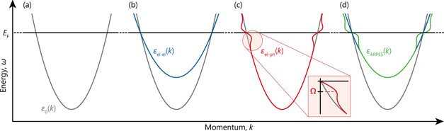
Figure 2. Schematic illustration of band renormalization effects. (a) Non-interacting 'bare' dispersion based on the free electron model, given by  . (b) and (c) Renormalized electronic dispersion due to the electron–electron interactions and the electron–phonon interactions, as indicated by the blue line [
 ] and red line [
 ], respectively, starting from
  . (d) Expected ARPES dispersion [
 ] in the presence of both electron–electron and electron–phonon interactions. Based on reference [12].
Download figure:
Standard image High-resolution imageSuch band renormalization effects have been often evaluated in terms of the electron self-energy. As seen in equation (2), the momentum distribution of the spectral function at constant energy becomes a Lorentzian function assuming the k-dependence of the self-energy is negligible, i.e.,  . Therefore, the analysis of the momentum distribution curve (MDC) is typically adopted to extract real and imaginary part of the self-energy,
  and
and  , where v0 is the group velocity of the bare band
  and Δk is the MDC half-width [1]. On the other hand, the analysis of the energy distribution curve becomes useful in the case of a flat band. However, the extraction of the self-energy is not trivial because it requires assuming an unknown bare band. Thus, the self-consistency of the self-energy via Kramers–Kronig relation has been often used as the empirical criterion of validating the extracted self-energy [68–72]. Moreover, iterative fitting algorithms for the determination of the bare band have also been developed based on the maximum entropy method [73–75] or the Kramers–Kronig relation [76–78]. In this review, we will not go into the details of such sophisticated methods and the validity of the bare band. Instead, we introduce a rather simple and widely used procedure to extract the self-energy, where we model the bare band within the one-electron picture [local density approximation (LDA) calculations]. On the other hand, care should be taken on the fact that measured ARPES spectra [
 ] reflect all the interactions working on the electrons as shown in figure 2(d), indicating necessity to decompose and evaluate each of contributions from different types of interactions. Indeed, it has also been proposed that the 'effective' electron–boson coupling strength is smaller than 'true' coupling strength because of the presence of the electron–electron coupling [79, 80]. However, many ARPES experiments have regarded the bare band as a renormalized band due to the electron–electron coupling, which has enabled evaluation of the 'effective' bosonic self-energy and coupling strength [68–72, 81, 82]. Nevertheless, the term 'effective' is sometimes abbreviated or overlooked. With the above in mind, we will demonstrate how high and low energy-scale interactions can be disentangled and evaluated by high-resolution ARPES in single-layer ruthenate Sr2RuO4, which is known as a representative strongly correlated electron system.
The Sr2RuO4 has attracted worldwide interest as the first reported layered perovskite superconductor without copper since the discovery of the superconductivity (Tc ∼ 1.5 K) in 1994 [83]. Furthermore, the ruthenate has been a strong candidate for the spin-triplet p-wave superconductivity [84], as evidenced by the experimental observation of the invariance of the Knight shift in the superconducting state [85]. Conversely, recent nuclear magnetic resonance experiments revealed a substantial reduction of the Knight shift [86]. It was also confirmed that the radiofrequency pulse causes the heat-up effect of the sample, which leads to the destruction of superconductivity and the non-reduction of the Knight shift as initially reported [85]. While the superconductivity of Sr2RuO4 is thus likely of singlet character, the quest continues to understand what exactly that the unconventional superconducting states of Sr2RuO4 might be. To clarify the physics behind the unconventional superconductivity of Sr2RuO4, it is thus essential to understand the normal metallic states and underlying electronic structure, from which the superconductivity emerges.
The crystal structure of Sr2RuO4 is the K2NiF4 with the space group I4/mmm body-centered tetragonal [figures 3(a) and (b)]. While it is isostructural to the cuprates, the crystal symmetry of the ruthenate remains high persistently even at lower temperatures without structural phase transitions and lower-symmetry orthorhombic structures. In addition, the ruthenate is chemically stable, and the oxygen content must be very close to stoichiometry. Thus, the valence of the ruthenium should be 4+, forming the metallic ground states with the Ru 4d4 low-spin electronic configuration, as shown in figure 3(c), where four 4d electrons partially occupy t2g
(dxy
, dyz
, dzx
) orbitals, but eg
orbitals are fully unoccupied because the energy difference between t2g
and eg
energy levels, i.e., a crystal field splitting 10 Dq is sufficiently large (∼3 eV). The transport property of Sr2RuO4 in the normal state can be well described by the Fermi liquid picture: both in-plane and out-of-plane resistivity follows T2 dependence below 25 K, while two-dimensional electrical conductivity is expected because of the large anisotropy (ρc
/ρab
∼ 1000). The basic electronic structure and Fermi surface of Sr2RuO4 are well described by theoretical calculations. Figure 3(e) shows the calculated electronic structure based on the LDA without the spin–orbit interaction (SOI) along the high-symmetry points [see figure 3(d)]. Two Ru 4d bands (dxy
and dzx
) cross EF along the ΓM and ΓX directions and enclose the occupied electronic states centered at the Γ/Z point, thereby forming two electron-like sheets centered at the Γ/Z point labeled as β and γ from the inside. Remaining one Ru 4d t2g
band (dyz
) crosses EF only along the ΓX direction, and encloses the unoccupied electronic states centered at the X point, forming one hole-like sheet (labeled as α). Thus, the α, β, and γ sheets are mainly composed of the dyz
, dzx
, and dxy
bands, respectively, except for the zone diagonal (ΓX), where three bands have small kz
modulation leading to the crossing points between the β and γ (γ and α) bands in the absence of the SOI [figure 3(f)]. However, these band-degeneracies are lifted by the SOI, so that three Fermi surfaces become separated with a significant reduction of three-dimensionality, leading to the quasi-one-dimensional α and β sheets as well as the two-dimensional γ sheet [figure 3(g)]. Indeed, the LDA calculations, including the SOI, resulted in the closer reproducibility on the Fermi surface topology observed by ARPES and de Haas–van Alphen (dHvA) experiments [87, 88]. On the other hand, the effective mass (m*) determined by dHvA experiments were much heavier than the LDA band mass (mLDA), indicating the strong electron correlation:  [84]. However, this poses an embarrassing question as to why the largest mass enhancement emerges in the γ sheet derived mainly from the widest dxy
band (Wxy
∼ 3 eV), and not in the α nor β sheets from the narrow dyz
and dzx
bands, respectively (Wyz,zx
∼ 1 eV). Thus, the orbital dependent mass enhancement cannot be simply explained by the electron correlation, placing importance to evaluate high and low energy-scale renormalization effects.
[84]. However, this poses an embarrassing question as to why the largest mass enhancement emerges in the γ sheet derived mainly from the widest dxy
band (Wxy
∼ 3 eV), and not in the α nor β sheets from the narrow dyz
and dzx
bands, respectively (Wyz,zx
∼ 1 eV). Thus, the orbital dependent mass enhancement cannot be simply explained by the electron correlation, placing importance to evaluate high and low energy-scale renormalization effects.
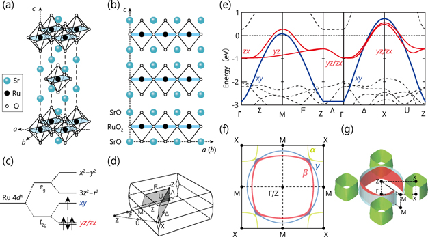
Figure 3. Crystal structure, electronic configuration, band structure, and Fermi surface of Sr2RuO4. (a) and (b) Crystal structure of Sr2RuO4 in an aerial and a cross-sectional view, respectively. (c) Electronic configuration with crystal field splitting. (d) Three dimensional BZ of body-centered tetragonal. (e) and (f) Band-structure calculations based on the LDA [152]: (e) band dispersion and (f) Fermi surface projected into two dimensional space. (g) Three dimensional Fermi surface calculated from the LDA with SOI [88]. Based on reference [12].
Download figure:
Standard image High-resolution image3.2. High energy-scale renormalization
Band renormalization in a high energy-scale regime is mostly dominated by the electron correlation—the interaction between the electrons. As the electron–electron interaction renormalizes the whole electronic band, it is necessary to observe an electronic band in a wide energy range, to evaluate the electron correlation properly. However, this is not always straightforward, especially in the strongly correlated systems, because the spectra become broader toward high energy region due to increasing scattering with energy. Besides, in the multiband systems, the band position might not be accurately trackable due to the proximity of several bands. Then, the utilization of linear polarization is useful not only to determine the symmetry of observed states but also to simplify observable electronic bands by sorting out the orbital symmetry of the initial-states based on the dipole selection rule [2]. The heart of the selection rule of the initial state is based on the dipole matrix element,  , where
  is the initial-state (final-state) electron wave function, and
A
and
p
are the vector potential and momentum operator, respectively. To detect the photoelectrons emitted in the mirror plane (
is the initial-state (final-state) electron wave function, and
A
and
p
are the vector potential and momentum operator, respectively. To detect the photoelectrons emitted in the mirror plane ( ), the overall matrix element and
  should be even, and thereby,
  must have the same symmetry as the dipole operator
A
⋅
p
. In other words, the even-symmetry initial states are only observable when
must have the same symmetry as the dipole operator
A
⋅
p
. In other words, the even-symmetry initial states are only observable when  (p-polarization geometry), whereas the odd-symmetry initial states are only observable when
  (s-polarization geometry).
The Fermi surface of Sr2RuO4 shown in figures 4(a) and (b) were respectively measured in the p- and s-polarization geometry, where the spectral-weight distribution of the Fermi surface sheets strongly depends on the polarization geometry, especially along the zone horizontal (Γ–M) and diagonal (Γ–X). Focusing on the Γ–M high-symmetry, two dzx and dxy bands exist closely along there, making it difficult to accurately determine each of dispersion in the wide energy range [89]. In contrast, these two bands can be selectively observed with p- and s-polarization geometry, as shown in figures 4(c) and (d). It should also be noted that the optimization of the excitation energy is also indispensable to observe and determine the band dispersion in a wide energy range [90]. By comparing the ARPES (circles) and LDA dispersions (lines), the high energy-scale band renormalization effects seem to be orbital-dependent. In general, the band renormalization caused by the electron correlation has been considered to result in the band narrowing as observed for the dzx band, where the group velocity (effective mass) is entirely slower (enhanced) than that of the LDA dispersion. However, the dxy band shows slower and faster group velocities compared with the LDA dispersion at the respective energies above and below the intersection of their dispersions. In addition, the dxy band exhibits a vertical dispersion near the intersection of the ARPES and LDA dispersions. This dispersion pattern, like a waterfall, is a key signature of the high energy anomaly (HEA) as widely reported in cuprates experimentally and theoretically [91].

Figure 4. High energy-scale band renormalization in Sr2RuO4. (a)–(d) Fermi surface ((a) and (b)) and ARPES image plot ((c) and (d)) observed along the high symmetry ΓM line in the p- and s-polarization geometry, respectively. The ARPES dispersions were determined by fitting the momentum distribution curves, except for the flat dispersion around the bottom of the dzx
band, which was determined by fitting energy distributions curves. (e) and (f) Real and imaginary parts of the self-energy  (open circles) and
  (filled circles) for the dzx
and dxy
band, respectively. Solid and dashed lines in blue (red) represent the real and imaginary parts of the model self-energy [
(filled circles) for the dzx
and dxy
band, respectively. Solid and dashed lines in blue (red) represent the real and imaginary parts of the model self-energy [ and
and  ] obtained by fitting
  . (g) and (h) Calculated spectral functions for the dzx
and dxy
band, respectively, where LDA dispersion is used as the bare dispersion and the real and imaginary parts of the model self-energy in (e) and (f) are used. Panels (a) and (b) are based on reference [99], and the rest on reference [90].
. (g) and (h) Calculated spectral functions for the dzx
and dxy
band, respectively, where LDA dispersion is used as the bare dispersion and the real and imaginary parts of the model self-energy in (e) and (f) are used. Panels (a) and (b) are based on reference [99], and the rest on reference [90].
Download figure:
Standard image High-resolution imageTo visualize the band renormalization effects, the real and imaginary part of the self-energy [ and
and  ] of the dzx
and dxy
bands were derived using the LDA dispersion as the bare band, as shown respectively in figures 4(e) and (f). In contrast to the observed two distinct types of band renormalization effects, the experimental self-energies (filled and open circles) of both dzx
and dxy
bands can be reasonably explained by a simple analytic model (solid and dashed lines) [90], given by
] of the dzx
and dxy
bands were derived using the LDA dispersion as the bare band, as shown respectively in figures 4(e) and (f). In contrast to the observed two distinct types of band renormalization effects, the experimental self-energies (filled and open circles) of both dzx
and dxy
bands can be reasonably explained by a simple analytic model (solid and dashed lines) [90], given by

where λel is the coupling constant of the electron–electron interaction and ωc is a characteristic energy of the model self-energy as discussed below. The validity of the model is also supported by the fact that the simulated spectral functions well reproduce the global spectral shapes and intensities, as seen in figures 4(g) and (h). Importantly, this functional form can be deduced from two generic assumptions (for details, see supplementary information of reference [90]): (1) ω2-dependence near the Fermi level to satisfy the Fermi liquid theory, and (2) the zero-convergence at infinite energy, i.e.,  , to satisfy the causality. Then, the real and imaginary part of the model self-energy is expressed as

satisfying the Kramers–Kronig relation. As seen in equation (12), there exists characteristic energy (ω = ωc) at which the real part becomes zero ![$\left[{{\Sigma}}_{\mathrm{el}}^{\prime }\left({\omega }_{\mathrm{c}}\right)=0\right]$](https://content.cld.iop.org/journals/2516-1075/2/4/043001/revision2/estabb379ieqn50.gif) and the imaginary part has a local minimum
and the imaginary part has a local minimum ![$\left[{{\Sigma}}_{\mathrm{el}}^{{\prime\prime}}\left({\omega }_{\mathrm{c}}\right)=-2{\lambda }_{\mathrm{el}}{\omega }_{\mathrm{c}}\right]$](https://content.cld.iop.org/journals/2516-1075/2/4/043001/revision2/estabb379ieqn51.gif) . The energy scale of the HEA should be given by the ωc, where the sign of the
. The energy scale of the HEA should be given by the ωc, where the sign of the  reverses, thereby making the dispersion shape vertical-like near the ωc, and the spectral weight is also suppressed due to the enhanced linewidth broadening. In the present case, the energy-scale of the HEA (ωc = 1.2 eV) agrees well with the reported on-site Coulomb interaction U = 1.2–1.5 eV [92, 93]. On the other hand, in most 3d transition metal oxides, the ωc might be related to the exchange interaction J because U is typically much larger than the bandwidth (U >> W) as the reported energy scales of the HEA (0.3–0.6 eV) are indeed similar to 3J = 0.35 eV in the case of cuprates [94].
Irrespective of an exact origin determining the ωc, present results highlight two distinct types of band renormalization depending on the energetic relationship between the ωc and bare band-bottom energies (ω0). One type, observed in the dzx
band, yields only band narrowing associated with the increased effective mass, because  so that the positive part of the
  is only involved for the band renormalization. The other type, observed in the dxy
band, also yields the effective mass enhancement for
is only involved for the band renormalization. The other type, observed in the dxy
band, also yields the effective mass enhancement for  , while the band-bottom energy is reduced, leading to a larger W. This is just because
  so that the positive and negative parts of the
  are both involved in the band renormalization, accompanied by the emergence of the HEA near the ωc. The profound implication is that effective mass enhancement is not always simply measured by U/W [95]. Indeed, the high energy-scale mass enhancement, 1 + λel, was estimated to be about three times heavier compared with the LDA band mass regardless of the significant difference of their bandwidth (Wxy
and Wzx
). It should also be emphasized here that the presence of the ωc should be a common feature for the electron self-energy, as long as the imaginary part of the self-energy has some energy dependence irrespective of its functional form in the low-energy region, which yields a hump structure (local minimum) due to the constraint of the zero-convergence at infinite energy. Therefore, the HEA and band narrowing should be a ubiquitous electronic feature as the high energy-scale band renormalization in the system with
are both involved in the band renormalization, accompanied by the emergence of the HEA near the ωc. The profound implication is that effective mass enhancement is not always simply measured by U/W [95]. Indeed, the high energy-scale mass enhancement, 1 + λel, was estimated to be about three times heavier compared with the LDA band mass regardless of the significant difference of their bandwidth (Wxy
and Wzx
). It should also be emphasized here that the presence of the ωc should be a common feature for the electron self-energy, as long as the imaginary part of the self-energy has some energy dependence irrespective of its functional form in the low-energy region, which yields a hump structure (local minimum) due to the constraint of the zero-convergence at infinite energy. Therefore, the HEA and band narrowing should be a ubiquitous electronic feature as the high energy-scale band renormalization in the system with  and
and  , respectively.
Finally, it should be noted that both two-types of high energy-scale band renormalizations lead to the significant but similar strength of effective mass enhancements, indicating that the electron correlation cannot explain the orbital-dependent mass enhancement of Sr2RuO4. On the other hand, one may notice an apparent deviation between the experimental and model self-energies in the low-energy region in the case of the dxy band, while not in the dzx band. This low energy-scale band renormalization, due to the electron–boson interaction as well as the SOI, should be crucial to understand the orbital-dependent mass enhancement, as we will discuss in the next section.
3.3. Low energy-scale renormalization
As already mentioned in figure 2(d), the observed ARPES spectra includes all the interaction information. Hence, proper treatment of high energy-scale renormalization effects is necessary to evaluate the low energy-scale interaction quantitatively. Figure 5(a) illustrates a standard procedure to extract the real part of the self-energy, where we assume two scattering channels, the electronic and bosonic interactions. These interactions are nearly independent in the scattering process because of their different energy-scales, and hence the Matthiessen's rule holds [96]. The real-part of the total self-energy (Σtot') can be thus written as the summation of these interactions,

which explains the energy-band renormalizations shown in figure 5(a): the bare dispersion  (black) is renormalized due to the electronic interaction in the wide energy range resulting in
  (gray), and further renormalized by the bosonic interaction near the Fermi level resulting in
  (cyan) corresponding to what is measured by ARPES. Then, the real part of the self-energy due to the bosonic interaction as

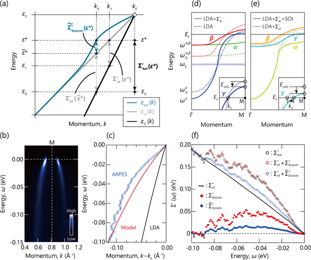
Figure 5. Low energy-scale band renormalization in Sr2RuO4. (a) Schematic illustration of the band renormalization due to the electron–electron and electron–boson interactions near the Fermi level. (b) ARPES data measured at 42 eV along the ΓM line with s-polarization geometry. (c) The γ-band dispersion obtained by fitting MDCs (blue circles), compared with the model dispersion (red) and LDA dispersion (black). The model dispersion includes band renormalization effects due to the electron–electron and the spin–orbit interactions. (d) and (e) Schematic band dispersions along the ΓM line based on LDA + Σel' and LDA + Σel' + SOI calculations, respectively. (f) The real-part of the self-energies derived from various methods. Based on reference [97].
Download figure:
Standard image High-resolution imageAlso, the group velocities of  and
and  are given by

Then, the coupling strength of the electron–electron interaction (λel) can be defined as

within the effective mass approximation. Now, we can rewrite equation (14) using the λel as

Here we introduced the 'effective' real part of the self-energy  , which represents the energy shift due to the electron–boson interaction from the energy
  renormalized by the electron–electron interaction. From the differential of equation (17), the coupling strength can be written as

where we used  and
and  . Moreover, similar discussions (for details, see supplementary information of reference [97]) can provide the relationship about the imaginary part of the self-energy as

In a conventional procedure, the bare band is assumed by an approximated band by fitting a simple function (linear, polynomial, etc) to the  in the energy region higher than the bosonic mode energy. As clearly indicated by equations (17)–(19), the magnitude of the 'effective' self-energy and coupling strength is reduced by a factor of
  compared with the 'true' self-energy. It should be noted that the real and imaginary parts of the 'true' self-energy are related via the Kramers–Kronig transformation as

where P denotes the Cauchy principal value of the integral. This implies that the 'effective' self-energy should also satisfy the Kramers–Kronig relation and that such self-consistency does not solely guarantee the validity of the bare band as well as the magnitude of the self-energy. Therefore, for the proper evaluation of the 'true' electron–boson interaction in the low energy-scale, it is indispensable to account for the electron–electron interaction in the high energy-scale.
As an application example of the above methodology, the evaluation of the strength of the electron–boson interaction in Sr2RuO4 will be shown. The γ band dispersion can be accurately determined by the MDC analysis on the polarization-dependent ARPES data measured along the ΓM line with the s-polarization geometry [figure 5(b)]. Figure 5(c) compares the γ band dispersion derived from ARPES (blue circles), model calculations (red line) and LDA calculations (black line), giving the estimation of the coupling strengths of the electronic and bosonic interactions (λel and λboson).
Here, the model calculations empirically include the electronic renormalization effects in two-steps as schematically drawn in figures 5(d) and (e): (1) the model self-energies due to the electron–electron interaction is first applied to the three Ru t2g LDA bands, resulting in the LDA + Σel' dispersions [figure 5(d)], and subsequently, (2) the orbital hybridization is generated by the inclusion of the SOI at/near the degenerated or crossing points, resulting in the LDA + Σel' + SOI dispersions [figure 5(e)]. These two-step renormalizations accompany considerable electronic modifications near the Fermi level: (1) the lowering of the energy of the van Hove singularity (EvHS) [figures 5(d) and (e)], and (2) the charge transfer from the β band to the γ band, leading to the expansion (shrink) of the Fermi momentum (kF) for the γ (β) band as shown in figure 5(e). The energy location of the EvHS is significantly important to estimate the strength of the electronic renormalization effects, as discussed later.
Accordingly, based on the present model, the electronic and bosonic interactions can be separately estimated from the effective mass of the ARPES and model dispersion of the γ band:  ,
,  , and λboson = λtot − λel = 1.2. Also, the coupling constant of the 'effective' bosonic interaction can be given by
  . Thus, one can see these estimates satisfy the relation given by equation (18) [
 ].
].
As shown in figure 5(f), the real part of the self-energies  can also be extracted from
  ,
,  , and
, and  dispersions as
  ,
,  , and
, and  . At a glance, one can see that the summation of
  and
and  is completely different from
  , i.e.,
  , re-confirming that the conventional procedure extracts not the 'true' but 'effective' self-energy. Indeed, the summation of
  and
and  precisely coincides with
  , where
  is derived from
  multiplied by
  with
with  . Also, the coupling strengths derived from the derivative of the real part of the self-energy at the Fermi level are λtot = 3.1, λel = 2.0, λboson = 1.1, and
  = 0.4, all consistent with those estimated from the effective mass enhancement. Note that the effective mass enhancement (
 ) is comparable to one determined by dHvA experiments (
 ), where the value is referenced from the present LDA dispersion. Note that a better agreement can be obtained if the instrumental resolution was considered (
 ) [97]. All these consistencies reasonably validate the present self-energy analysis in disentangling the coupling strength of high and low energy-scale interactions.
On the other hand, a recent laser-based ARPES study combined with single-site dynamical mean-field theory (DMFT) claimed that the low-energy renormalization including the kink of the γ band dispersion is not originated in the bosonic interaction but the electronic interaction, that is, the enhanced SOI ( ) due to the electron correlation by a factor of two compared with the bare one (
 ) [30]. Furthermore, the Fermi surface of ARPES and theoretical calculations show a remarkable consistency. However, on the other hand, another DMFT study [98] showed that the electron correlation enhances the magnitude of the SOI, while the total strength can be effectively suppressed depending on the quasiparticle renormalization. Thus, the SOI has energy dependence as

where  is the renormalization factor. Specifically, the effective coupling
  for
for  and
and  . Indeed, we have also found a similar reduction of the effective coupling at the Fermi level
  , to reproduce the experimental Fermi momentum of the γ band in the LDA + Σel' + SOI model calculations as ∼60 meV [97]. In addition, the van Hove singularity, shown in the DMFT calculations in reference [30], locates in the very vicinity of the Fermi level as
  , which is even closer to the experimental observation
  [99]. This contradiction is most likely originated in the over-estimation of the electronic renormalization due to the constant (energy-independent) and large effective SOI used in reference [30]. Therefore, to resolve above controversy and pin down the origin of the low energy renormalization effects in Sr2RuO4, it is necessary to examine agreement between experiment and theory on extended band structures, covering the low- to high-energy regions as well as the wide momentum space. The energy-dependent SOI and quasiparticle renormalization should also be included in further consideration.
4. Spatially-resolved ARPES on cuprates
4.1. Overview
Following rapid developments of micro- and nanoscale electronic devices these days, demands for characterization tools of understanding local electronic and magnetic properties at smaller length-scales have been growing toward a further miniaturized device with high performance and functionality as well as low power consumption. For studying localized electronic properties, there are two detection methods of photoemissions based on microscopy (parallel imaging) and spectromicroscopy (sequential acquisition of photoelectrons) [100].
The representative of the former technique is a photoemission electron microscope (PEEM), which measures a projected image of the spatial intensity distribution of photoelectrons I(x, y) simultaneously without scanning the sample. A broad photon beam illuminates the surface, and the image is then magnified by electron optics consist of electrostatic or magnetic lenses. Thus, the spatial resolution is solely determined by the chromatic and spherical aberrations of the electron lens system, typically well below 100 nm. Furthermore, PEEM can operate in micro-ARPES mode by implementing an energy filter [101], and enable imaging the two-dimensional I(kx
, ky
) momentum space at constant energy with a selected micron-order area (hear and hereafter, we omit kz
for simplicity of notation). However, the energy and angular (momentum) resolutions of such energy-filtered PEEM are limited to about a few 100 meV and  , respectively, and less flexibility on energy scan is bottleneck for practical use. Recently, these problems have been revolutionary improved by the development of momentum microscope, which combines a typical PEEM column and hemispherical deflection analyzer (HDA) enabling the fast acquisition of the three-dimensional images I(Ek
, kx
, ky
). The state-of-the-art momentum microscope with the double imaging HDAs enabled micro-ARPES operation with high energy and momentum resolution (12 meV and 0.005 Å−1) [102, 103]. Moreover, there are many advantages such as outstandingly efficient I(Ek
, kx
, ky
)-imaging by collecting all photoelectrons emitted into the complete solid angle above the sample surface, easily exchangeable operation between real-space and momentum-space imaging, and extensibility for spin-filtered and/or time-of-flight momentum microscope toward spin-resolved and/or time-resolved ARPES experiments. Nevertheless, there exists a severe restriction on measurable samples in these PEEM-based microscopes as they require a flat surface with homogenous illumination, which is hardly achieved, particularly when the surface is prepared by mechanical cleaving. In this viewpoint, spatially-resolved ARPES is a complemental spectromicroscopic technique because it can apply to a somewhat rough surface. Besides, spatially-resolved ARPES also has advantages on ultimate energy resolution as well as sub-micron spatial resolution, and hence, for studying Fermiology, many-body physics, and superconductivity. In the following sections, capabilities of spatially-resolved ARPES will be demonstrated by presenting a laser-based micro-ARPES study on a homogeneous surface system and nano-ARPES study on an inhomogeneous surface system using synchrotron radiation, after the general description on principle and instrumentations of spatially-resolved ARPES technique.
, respectively, and less flexibility on energy scan is bottleneck for practical use. Recently, these problems have been revolutionary improved by the development of momentum microscope, which combines a typical PEEM column and hemispherical deflection analyzer (HDA) enabling the fast acquisition of the three-dimensional images I(Ek
, kx
, ky
). The state-of-the-art momentum microscope with the double imaging HDAs enabled micro-ARPES operation with high energy and momentum resolution (12 meV and 0.005 Å−1) [102, 103]. Moreover, there are many advantages such as outstandingly efficient I(Ek
, kx
, ky
)-imaging by collecting all photoelectrons emitted into the complete solid angle above the sample surface, easily exchangeable operation between real-space and momentum-space imaging, and extensibility for spin-filtered and/or time-of-flight momentum microscope toward spin-resolved and/or time-resolved ARPES experiments. Nevertheless, there exists a severe restriction on measurable samples in these PEEM-based microscopes as they require a flat surface with homogenous illumination, which is hardly achieved, particularly when the surface is prepared by mechanical cleaving. In this viewpoint, spatially-resolved ARPES is a complemental spectromicroscopic technique because it can apply to a somewhat rough surface. Besides, spatially-resolved ARPES also has advantages on ultimate energy resolution as well as sub-micron spatial resolution, and hence, for studying Fermiology, many-body physics, and superconductivity. In the following sections, capabilities of spatially-resolved ARPES will be demonstrated by presenting a laser-based micro-ARPES study on a homogeneous surface system and nano-ARPES study on an inhomogeneous surface system using synchrotron radiation, after the general description on principle and instrumentations of spatially-resolved ARPES technique.
The principle of spatially-resolved ARPES technique is essentially identical as scanning photoemission microscopy (SPEM), which typically employs a high-resolution hemispherical analyzer to measure photoelectron intensity from micro/nano-metric surface region illuminated by micro/nano-focused photon beam. SPEM-type instruments thus require the mechanical scanning of the sample followed by the sequential acquisition of the photoemission spectrum for the real-space imaging, meaning that the spatial resolution is restricted by the diffraction limit of the photon beam at best in contrast to PEEM-type instruments. Spatially-resolved ARPES technique is often referred to as micro-ARPES or nano-ARPES, depending on the spatial resolution. These techniques have been developed to integrate the microscopic ability of SPEM into a standard high-resolution ARPES instrument to enable precise and versatile measurement on the energy–momentum band structure. In contrast, SPEM instruments had been mainly used for studying the local chemical information, i.e., used as electron spectroscopy for chemical analysis (ESCA) [104].
Figure 6(a) shows the schematic experimental layout of spatially-resolved ARPES, consisting of focusing optics, precise motion-stage, and high-resolution hemispherical analyzer. These major components are required for ARPES mapping in the real- and k-space, as described below.
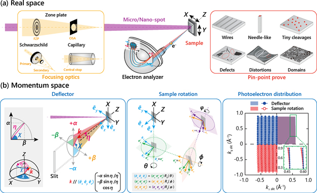
Figure 6. Schematic overview of spatially-resolved ARPES based on SPEM technique in the viewpoint of (a) real space and (b) momentum space. The incident light is focused down to micro/nano-spot through optical elements, enabling to acquire SPEM image by scanning the sample surface or to perform pin-point probe measurements on a tiny sample or region of interest by selecting a flat region or one of domains while avoiding defects and/or distortions. Mapping of the ARPES intensity in the in-plane momentum space can be achieved by utilizing the deflector-type electron analyzer (bottom-left) and/or by rotating the sample orientations (bottom-center). Here, the analyzer-manipulator arrangement can be defined by two types, type I and II, in which the analyzer slit is parallel and perpendicular to the manipulator rotary axis (θ-axis), respectively. (Bottom-right) Two-types of mapping by deflector or sample-rotation yield a slightly different photoelectron distribution in the momentum space, where the mappings were calculated for the type I (bottom-left) with the parameters: hν = 50 eV, Ekin = 45 eV, ϕ = 5 eV, ±10 deg for the acceptance angle of the detector in a vertical plane, and sample-rotation and deflector is scanned in a horizontal plane within a range of ±10 deg by a step of 2 deg. Each cut is represented by circles for the sample-rotation (red) and deflector (blue) mappings, and shaded area indicates the covering area. For simplicity, only half of acceptance angle (+5 or −5 deg) is shown in the left side (k⊥slit ⩽ 0), and the covering area and cuts for two mapping methods are compared in the upper and lower side, respectively, in the right side (k⊥slit ⩾ 0).
Download figure:
Standard image High-resolution imageFor nano-focusing of SX synchrotron radiation, a Fresnel zone plate (FZP) is installed at various beamlines in SOLEIL (ANTARES) [105], Diamond Light Source (I05) [12, 106], and Advanced Light Source (MAESTRO) [107], while a Schwarzschild objective based on two spherical mirrors is employed in ELETTRA (Spectromicroscopy) [108]. The focusing optics have to be carefully selected to meet demands for ARPES experiments: higher efficiency in terms of photon flux and practical energy resolution, wider availability of the photon energy, and a longer focal distance to reduce risk of clashing among components (optical/sample stages and electron analyzer). For instance, the FZP is diffractive optics having advantages on the spatial resolution as well as wider available photon energy [109], while its drawbacks are low focusing efficiency reducing flux significantly (∼1%) as well as the large chromatic aberration so that its focal length changes with the photon energy. In contrast, the Schwarzschild objective is achromatic optics providing higher efficiency (∼10%) to the FZP, though the available photon energy is restricted to a designed one. Existing nano-ARPES systems implemented these optics have been well developed and produced a growing amount of high-quality results. However, the typical energy resolution remains about 30 meV for practical usage due to the significantly reduced flux. This situation would be revolutionary changed by a novel capillary ellipsoidal mirror, which has been recently installed at the MAESTRO beamline [110, 111]. The capillary ellipsoidal mirror is achromatic optics with superior properties: high efficiency (∼60%), high numerical aperture, and long working distance. The available spatial resolution was evaluated as 250 nm at present, though it can also be improved down to about 100 nm with the refinement of manufacturing techniques in the near future. Note that, for the delivery of micro photon beam, Kirkpatrick–Baez mirrors are used at the MAESTRO beamline for micro-ARPES [112], a Wolter mirror is recently installed at the BL25SU beamline at SPring-8 for SX micro-ARPES [113], while optical lens system is employed in the case of the laboratory-based micro-ARPES system utilizing VUV laser [29, 114].
The overall spatial resolution of spatially-resolved ARPES is not solely determined by the illumination area of the micro/nano-focused photon beam onto the sample but also the accuracy and stability of the sample positioning. This makes a clear difference between spatially-resolved-type and standard-type ARPES instruments. In particular, for nano-positioning, implementation difficulty arises from a piezoelectric-driven stage as it is placed in situ and thereby should be non-magnetic and compatible with ultra-high-vacuum. On the other hand, for micro-positioning, the sample position within a measurement chamber can be controlled from ex-situ, similarly to the standard ARPES instruments, by utilizing a high precision XYZ manipulator with sub-micron accuracy [29]. With the combination of small spot and precise sample scanner, spatially-resolved ARPES can measure various types of systems: tiny samples (nanowires, nanoneedles), small cleavages embedded on the surface, partially flat portion selected from the homogeneous surface while avoiding defects and/or distortions, and one of the domains on the inhomogeneous surface. The typical procedure of spatially-resolved ARPES is briefly given below.
For the real-space imaging, ARPES spectrum I(Ek , kx , ky ) is sequentially measured by the high-resolution hemispherical electron analyzer while raster scanning along the lateral axes (x, y), and subsequently, the spatial distribution of the photoemission intensity I(x, y) can be obtained for specific energy Ek and momentum space (kx , ky ), typically with some integration windows. Note that the selection of (Ek , kx , ky ) provides a substantial advantage in the element/band/orbital selectivity in spatially-resolved ARPES experiments. After selecting the region of interest, based on the measured real-space imaging, the band mapping in the k-space is generally measured. There exist two ways to map out the emission-angle distribution of photoelectrons. One way is to utilize the deflector-type electron analyzer that has been recently developed. The deflector function enables to map out I(Ek , kx , ky ) without changing the orientation of the sample, that is, the geometric relationship is kept during the mapping. The photoemission intensity is measured as a function of two angular variables (α, β), which is the emission angle in parallel and perpendicular to the slit, respectively. The other way, which has been conventionally used, is to rotate the sample holder in situ, inevitably producing a displacement of a detection position on the sample surface. Although a computational compensation for the displacement can be possible [115], such rotational displacement becomes more problematic for the smaller spot-size as well as region-of-interest, indicating that the deflector function is intrinsically preferable for spatially-resolved ARPES.
Recently, Ishida and Shin have pointed out that the above two mapping methods should be formulated differently [116]. Indeed, the simulated momentum distribution of the photoelectrons provides a slightly different profile between the two mapping methods, as shown in figure 6(b). According to reference [116], the experimental configuration can be categorized by four types: type I with/without deflector and type II with/without deflector. The type I and II mean the arrangement of slit vertical and horizontal, that is, the analyzer slit is parallel (perpendicular) to the manipulator rotary axis, respectively. Figure 6(b) shows the configuration of type I with deflector, employed at the nano-ARPES endstation (I05, Diamond Light Source) [12, 106].
Following the notations used in reference [116], here we write down the photoelectron momentum
k
having angular spreads (α, β) toward the analyzer using unit vectors  and
and  , whose x–y plane is on the analyzer frame and crystal surface, respectively. The observing vector
k
in the analyzer's frame can be given by the two set of rotation (η and χ) for the scalar
, whose x–y plane is on the analyzer frame and crystal surface, respectively. The observing vector
k
in the analyzer's frame can be given by the two set of rotation (η and χ) for the scalar  pointing toward the z-axis. Two variables η and χ are defined in the polar-angular notation, as shown in figure 6(b), where
  and tan χ = β/α. More concretely, the direction of
k
is given by (1) rotation by
and tan χ = β/α. More concretely, the direction of
k
is given by (1) rotation by  along the
  axis, followed by (2) rotation by χ along the
  axis:
axis:

where sine and cosine functions are abbreviated as 's' and 'c', respectively, and  and
and  are the rotational matrices given by

For more general description, the rotations of the sample should be taken into account in the form of  [see also the inset of the bottom-center panel of figure 6(b)]. We can thus rewrite equation (22) as

where sχ and cχ were replaced by using  and
and  , and
, and  ,
,  , and
, and  are the rotational matrices given by

Based on equation (23), by replacing β = 0 and η = α in the case without deflector, and/or  to
to  for exchange from type I to type II, the photoelectron momentum for all the four types can be thus given as following:
where T1wD (T2wD) stands for the type I (II) with deflector and T1w/oD (T2w/oD) for the type I (II) without deflector. As an example, we calculated the photoelectron distributions for T1wD and T1w/oD, as shown in the right panel of figure 6(b), where one can see that two mapping ways using deflector or sample rotation can provide essentially the same distributions. However, caution might be taken for a slight but finite difference, which may affect quantitative analyses and discussions, e.g. on the shape and size of Fermi surfaces.
4.2. Laser-based micro-ARPES
A simple but significant benefit of a smaller beam spot is to improve the spectral quality by avoiding surface defects. In this section, we will demonstrate it by showing micro-ARPES results from Bi-based high-Tc cuprate superconductor Bi2Sr2CaCu2O8+δ (Bi2212) [29]. The crystal structure of Bi2212 is a layered structure composed of BiO-, SrO-layer, and CuO2 bilayer block as schematically drawn in figure 7(a), where a pair of BiO-layers are bonded by a van-der-Waals force, much weaker than other bonds. Thus, Bi2212 samples are expected to be cleaved between the Bi–O layers along the c-axis, resulting in a homogeneous surface composed of a single type of termination as a natural cleavage plane. However, the cleaved surface of Bi2212 can be easily distorted or bent due to its 'soft' crystal structure. Hence, micro-ARPES is especially useful to pinpoint a better portion of the surface by avoiding surface defects.

Figure 7. High-resolution micro-ARPES results from overdoped Bi2212 (Tc = 85 K) taken with 6.36 eV at 12.5 K using laser micro-ARPES system at HiSOR, Japan [29]. (a) Schematic crystal structure of Bi2212. (b) Schematic drawings of micro-ARPES geometry used for data acquisition shown in (c)–(f), and of Fermi surface of Bi2212 where the red line indicates the measured k-region along the nodal direction. (c) Surface image obtained by (upper) a SPEM and (lower) an ex-situ optical microscope. (d) Spatial distribution of (top) peak amplitude, (middle) peak center, and (bottom) peak width of ADCs (EF ± 10 meV) of ARPES spectra, measured at each position. All the values are rescaled by each mean value. (e) and (f) High-statics nodal ARPES data taken at the micro-spot indicated by the circle in the bottom panel of (d): (f) ARPES image and (e) its MDC at EF (circles) together with the Lorentzian function fit (red line). Panels (c)–(f) are based on reference [29].
Download figure:
Standard image High-resolution imageExperimental geometry used in the present micro-ARPES measurements is shown in figure 7(b), where an incident angle of the micro-focused laser (<5 μm) is 45 deg to the analyzer focal direction (Z-axis), and the sample was rotated around the X-axis (θ-rotation) toward the incident path. The electronic structure of Bi2212 near the Fermi level is occupied by the Cu  and O 2p states, forming the bilayer-split Fermi surfaces of antibonding and bonding band (AB and BB). We focus on the nodal direction [(0, 0)–(π, π)], as indicated by the red line on the schematic Fermi surface of Bi2212 in figure 7(b). Along this line, both the superconducting gap and pseudogap become minimum or zero [1, 117], making analysis and interpretation more straightforward than the data taken at other k-space. Also, a low excitation energy (<7 eV) and s-polarization geometry were employed to enable a selective observation of the isolated AB band [blue line in figure 7(b)] while suppressing the BB [57, 118]. With this configuration, we mapped out the spatial distribution of the ARPES intensity by sequentially measuring the ARPES spectrum while changing X- and Y-coordinates. Figure 7(c) displays an obtained spatial map covering the whole sample surface with step sizes of 100 × 100 μm2, where each pixel intensity represents the integrated spectral weight of the nodal ARPES spectrum [similar to figure 7(f)] over the whole energy and angular windows at each position. Such spatial ARPES intensity map is often called as a scanning photoemission microscope (SPEM) image, which can capture spatial features of the cleaved surface, comparable to an ex-situ optical microscope image. It is obvious that surface region near the upper-right side is largely distorted and cracked, and thus, unsuitable for ARPES measurements. While the other area is fairly flat with homogeneous intensity distribution, it makes it rather difficult to pick up the most suitable position for further fine measurements, just relying on the intensity profiles. To resolve this dilemma, we then propose an effective method based on an ADC-analysis (ADC: angular distribution curve).
We selected a 100 × 100 μm2 region, indicated by the square on the SPEM image in figure 7(c), as the best portion on the surface using the same method as described below. We analyzed the ADC at the Fermi level along the nodal direction in Bi2212 [similar to figure 7(e)] using the Lorentzian function. By fitting the ADC at each coordinate, we determined the spatial distribution of the peak amplitude (PA), peak center (PC), and peak width (PW) of the Lorentzian function within the 100 × 100 μm2 region with five μm steps both in the X and Y axes, as summarized in figure 7(d). Those values show significant fluctuations of about ±20% against the mean value. While the intensity fluctuations appear randomly in the PA image, the PC and PW spatial distributions present a similar two-domain-like feature though they contain quite different information. While the PC is directly related to the emission angle, its absolute fluctuation is indeed smaller than 0.5 deg, meaning that the corresponding Fermi momentum (kF) is almost identical within the region of interest in the present case using the low excitation energy. Therefore, the pixel by pixel fluctuations in the PW image should reflect the local surface inhomogeneity, rather than the dopant inhomogeneity as reported by STM studies [119, 120]. Hence, the lower PW region is regarded as a more suitable region for acquiring intrinsic ARPES spectra in the present case as the PW is primarily due to the electron-impurity interaction at sufficiently low temperatures [68].
Then, we have measured high-statistic ARPES data on the selected micro-spot [red circle in figure 7(d)], where the PW shows a local minimum. As shown in figure 7(f), the high-quality of the ARPES data is demonstrated by the incredibly sharp MDC at the Fermi level, as shown in figure 7(e). The total peak width (ΔkT) of the MDC is 0.0038 Å−1, corresponding to a significantly long electron mean free path l > 260 Å. Here, we assume that the ΔkT is given by the convolution of the sample intrinsic MDC width (ΔkS) and the instrumental momentum resolution (ΔkI), represented by the Lorentzian and Gaussian functions, respectively. In other words, the ΔkT can be expressed by a Voigt function as  , and thereby
  . By fitting the Voigt function, each contribution was estimated as ΔkI ∼ 0.0006 Å−1 and ΔkS ∼ 0.00373 Å−1. Surprisingly, the present ΔkT is very close to the ΔkS (ΔkT ∼ 0.98ΔkS), owing to the negligible ΔkI. It should be noted that significantly high instrumental resolution ΔkI is realized owing to two factors; (1) superior angular resolution (ΔθI) better than 0.05° owing to the micro-focusing, and (2) low excitation energy (Ekin ∼ 1.8 eV) as ΔkI is given by 0.51231
  .
.
In summary, we demonstrated in this section that the micro-ARPES technique holds several significant advantages. First, micro-ARPES is generally compatible with a standard high-resolution ARPES setup, and hence, enables high-energy resolution ARPES measurements at low-temperatures typically below 10 K, without great sacrifices of the photon flux in contrast to the nano-ARPES technique introduced in the next section. Secondly, the micro-focusing greatly improves the instrumental angular resolution, enabling the observation of the sample intrinsic scattering rate. Thirdly, the micro-spot can yield a benefit for improving spectral quality by avoiding surface defects even on the homogeneous surface. All these indicate that the applications of micro-ARPES can extend far beyond the present study. Indeed, the micro-ARPES has been successfully applied to the study of the electronic structure of microscale materials/domains: high-Tc cuprates [121–124], high-Tc iron pnictides [125–127], and the two-dimensional vdW heterostructures [114].
4.3. SR-based nano-ARPES
In the previous section, we showed that micro-ARPES helps to obtain intrinsic electronic information with high accuracy by optimizing measurement position from a homogeneous surface, composed of a single termination but containing surface defects. However, this approach is still an extension of the standard ARPES technique. Here, we will introduce a specific capability of the nano-ARPES technique, allowing us to extract local electronic information from each micro-domain by characterizing/analyzing an inhomogeneous surface where multiple surface terminations coexist. As an example, we focus on the yttrium–barium–copper-oxide (YBCO) system, known as a complicated electronic system due to its unique crystal structure composed of not only two-dimensional CuO2 planes but also one-dimensional CuO chains.
The specific system introduced here is YBa2Cu4O8 (Y124), which contains two sets of CuO2-bilayer blocks and CuO-chain layers per unit cell, and is similar to the more familiar YBa2Cu3O7−d (Y123) possessing a single set of CuO2-bilayer block and CuO-chain layer. Figures 8(a) and (b) schematically illustrate the orthorhombic crystal structure of Y124 with the space group of Ammm in an aerial and a cross-sectional view, respectively [128]. Two CuO2-planes form a bilayer block with the insertion of Y atoms, and two CuO-chain layers also form a block along the b axis with edge-sharing each other, and thereby these blocks are stable. Remaining BaO layers are attracted toward the CuO2-bilayer block, making a relatively large vacancy between the CuO-chain and BaO layers. As a consequence, the Y124 crystals are generally expected to be cleaved above/beneath the CuO-chain block [dashed lines in figure 8(b)], yielding multiple surface terminations due to either the CuO-chains or BaO layers.
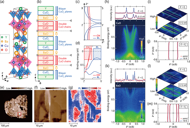
Figure 8. Nano-ARPES results from Y124 (Tc = 82 K) taken with 60 eV at 30 K using nano-ARPES system [106] of the I05 beamline [13] at the Diamond Light Source, UK. (a) and (b) Schematic crystal structure of Y124 in an aerial and a cross-sectional view, respectively. (c) Schematic Fermi surface derived from CuO-chain (CH: red) and CuO2-plane (PL: blue) bands. (d) Band dispersions along the high-symmetry ΓY line based on band-structure calculations [149]. (e) and (f) Overview SPEM images and (f) expanded SPEM image, respectively. The red rectangle in (e) indicates a region of interest zoomed in (f). (g) Spatial distribution of CuO-chain and CuO2-plane dominant regions (CH and PL), as indicated by the red and blue regions, respectively. (h) Termination-dependent ARPES image taken from the CuO-chain termination taken along the high-symmetry Y–Γ–Y line, together with the MDCs. (i) and (j) Constant energy maps and experimental kF plots of the CH bands for the CuO-chain termination. (k)–(m) Same as (h)–(j) except that they are for the BaO surface termination. Based on reference [106].
Download figure:
Standard image High-resolution image
Figure 8(c) shows a schematic Fermi surface of Y124 composed of CuO-chain bands (CH: red lines) and CuO2-plane bands (PL: blue lines) [128]. The ΓY/ΓX symmetry line is parallel/perpendicular to the CuO-chain direction, and the ΓS symmetry line is diagonal direction. We focus on the ΓY direction where two CH bands cross the Fermi level while PL bands locate deeper energy, as seen in the calculated band dispersions [figure 8(d)]. Figure 8(e) shows the overview SPEM image constructed from the integrated valence band intensity of Y124 obtained by entirely scanning the cleaved surface. Note that the observed intensity modulation should be related with not only intrinsic effects due to different surface terminations, but also extrinsic effects due to surface roughness (height fluctuations). To reveal the intrinsic intensity modulation, a narrow area on the surface [red square in figure 8(e)] was further investigated, where the height fluctuations are small (<1–3 μm), well below the focal depth of the nano-ARPES setup.
Figure 8(f) displays the expanded SPEM image with 500 nm fine steps, constructed from the integrated ARPES intensity near the Fermi level along the high-symmetry Y–Γ–Y line, making the information of the surface termination unclear. To uncover the separate contributions from the CuO-chains- and BaO-layer terminations, the spatial mapping data was re-constructed by utilizing narrow integration windows and by taking image intensity ratio. First, integration windows were determined to be sensitive to either CH or PL bands [red and blue boxes in figure 8(d)], yielding the two-dimensional intensity maps (ICH and IPL). Subsequently, the intensity ratio of the mean deviation between the CH and PL bands were deduced as  , where
  and
and  is the mean value of ICH and IPL, respectively. The resulting image is presented in figure 8(g), which highlights the dominant signal from the CH and PL bands in red and blue, respectively. As is evident, the ARPES signals were dominated by emission from the topmost surface layer: CH bands for the CuO-terminated surface and PL bands for the BaO-terminated surface. This interpretation is also supported by the observation of the chemical shift in the core-level spectra from each domain [106].
The termination-selected ARPES data were then observed on each surface termination, as shown in figures 8(h) and (k). On both terminations, two dispersive electronic features observed around the Γ point are originated in the CH bands. On the other hand, they show different behavior depending on the termination as also visualized in the MDCs. On the BaO-terminated surface, the metallic dispersions of double CuO chains were observed. The result is a sharp contrast to what was observed for the CuO-terminated surface, where the inner-chain band dispersion only crosses the Fermi level, while the outer-chain band does not. These distinct behaviors must be originated in the surface electronic reconstruction as the CuO-chain states arise from the subsurface CuO-chain layer beneath the CuO2 planes for the BaO-terminated surface while from the topmost CuO-chain layer for the CuO-terminated surface. Here, the double metallic CH bands on the BaO-terminated surface were observed for the first time by nano-ARPES, while each of the metallic and insulating CH band on the CuO-terminated surface was similarly reported in previous micro-ARPES studies [122, 124]. Note that the metallic CuO-chain states are more representative of the metallic bulk transport properties of the CuO-chains [129, 130] because they are free from exotic surface insulation effects seen in the topmost CuO chain exposed on the CuO-terminated surface.
The constant energy planes shown in figures 8(i) and (l) highlight again the termination dependence of the CuO-chain states, which can be confirmed in the broader region across the Brillouin zone. Figures 8(j) and (m) show the quasi-one-dimensional CuO-chain Fermi surfaces, precisely determined by fitting MDCs. From the warping of the Fermi surface, one can evaluate the in-plane charge transfer due to interchain and intrachain couplings by fitting the Fermi momentum plots using a simple tight-binding model given by  , where μ is the chemical potential, and ta
and tb
are hopping parameters across and along the chain, respectively [131]. The quasi-one-dimensional dispersions can be well reproduced by the model. The interchain hopping is found to be consistently small
, where μ is the chemical potential, and ta
and tb
are hopping parameters across and along the chain, respectively [131]. The quasi-one-dimensional dispersions can be well reproduced by the model. The interchain hopping is found to be consistently small  compared to the intrachain hopping
  for all CuO-chain bands, resulting in the large hopping anisotropy given by
  . On the other hand, such strong hopping anisotropy in the CuO-chain implies the strong one-directionality of the electron hopping, which may lead to characteristic one-dimensional electronic excitations such as Tomonaga–Luttinger liquid (TLL) or marginal Fermi liquid (MFL). However, the expected electronic behaviors were not observed in the vicinity of the Fermi level: the power-law depletion of spectral weight, given by
  , expected for TLL [132], nor the steep broadening of quasiparticle lifetime with a linear ω-dependence expected for MFL [133]. Therefore, the presence of the longitudinal hopping (tc
) is reasonably speculated. An orbital hybridization between the CuO-chain
, expected for TLL [132], nor the steep broadening of quasiparticle lifetime with a linear ω-dependence expected for MFL [133]. Therefore, the presence of the longitudinal hopping (tc
) is reasonably speculated. An orbital hybridization between the CuO-chain  orbitals and CuO2-plane
  orbitals via apical oxygen 2pz
orbitals was predicted based on more bulk-sensitive experiments on the analogous Y123 system using x-ray absorption spectroscopy and resonant inelastic x-ray scattering [134]. This interpretation is also in line with the three-dimensional metallic transport properties of Y124 [130].
orbitals via apical oxygen 2pz
orbitals was predicted based on more bulk-sensitive experiments on the analogous Y123 system using x-ray absorption spectroscopy and resonant inelastic x-ray scattering [134]. This interpretation is also in line with the three-dimensional metallic transport properties of Y124 [130].
Similarly to the above demonstration, the state-of-the-art nano-ARPES systems have been successfully revealed local electronic structures in various micro- and nano-scale systems: exfoliated micro-flakes in two-dimensional vdW heterostructures [135, 136], nanowires [137, 138], multiple domains/terminations in high-Tc superconductors [106, 139], and a side surface of a weak topological insulator β-Bi4I4 [140]. Furthermore, very recently, nano-ARPES studies with back-gate voltage have been successfully reported [141, 142], suggesting that nano-ARPES holds promise for realizing operando measurements and visualizing local electronic states on nanodevices under operation. On the other hand, it should also be noted that there still exists room for improvements in the nano-ARPES technique: experimental efficiency, available energy-resolution, and lowest-sample-temperature in nano-ARPES are typically worse than those in high-resolution ARPES or micro-ARPES. Together with the implementation of highly efficient focusing optics such as the recently developed capillary mirror [110, 111], continuous developments on these scopes will realize high-resolution nano-ARPES experiments at very low-temperature. Advanced nano-ARPES with high energy resolution and low-temperature will open a new playground to study the spatial distribution of physical parameters such as the coupling parameter of many-body interactions and superconducting gap.
5. Concluding remarks
We reviewed the principle, instrumentation, and capabilities of modern ARPES techniques with specific exemplary results obtained by the author. Although the present results were probably not sufficient to give an impression of the wide variety of applications of ARPES techniques, we hope a series of related results help the reader to understand the capabilities of modern and still growing ARPES techniques.
In the last few decades, energy and momentum resolutions of ARPES has been remarkably improved, enabling detailed investigations on electronic band structure, Fermi surface, energy-gap, and what is more, many-body interaction in a momentum resolved manner. On the other hand, it should be emphasized that the utilization of experimental degrees of freedom is essential to extract intrinsic electronic information efficiently in high-resolution ARPES experiments. In other words, it is significantly important to optimize the photon energy, polarization, and the orientations and temperature of the sample.
As one of the advanced ARPES technique, we introduced spatially-resolved ARPES, which had been developed to combine the advantages of conventional ARPES and the microscopic ability of SPEM by utilizing the micro/nano-focused light. Micro-ARPES system has already been sophisticated and achieved compatibility of high energy and momentum resolutions and micro-scale spatial resolution while keeping the flexibility of sample orientations and low-temperature. Nano-ARPES system has also been significantly developed and became a practical tool, especially by implementing the deflector-type analyzer. However, the available energy resolution still behind compared to high-resolution or micro-ARPES systems because of the reduced photon flux delivered by the focusing optics. On the other hand, such difficulty will be resolved in the near future with continuous efforts on developing focusing optics such as the novel capillary ellipsoidal mirror [110, 111]. We believe spatially-resolved ARPES will open an opportunity to study the wide variety of systems, including tiny samples, hardly-cleavable samples, polycrystalline samples, and inhomogeneous samples, all of which were extremely difficult to study by standard, spatially-integrated technique.
While not dealt with in this review, the material side is also crucial in ARPES experiments. The quality of the sample is directly related to the spectral width, and extra broadening may hinder capturing essential details of the electronic band structures. Therefore, it is vital to continuously improve sample synthesis techniques, such as in situ thin-film fabrication by MBE or PLD. In particular, the combination of ARPES and such a sample-growth system is an efficient platform to systematically design and synthesize new materials and properties based on their electronic structures. Moreover, it will have more attention to put external perturbation on the sample while measuring ARPES by applying uniaxial pressure [143–146] and gating-voltage [141, 142] for exploring and controlling novel emergent physical properties.
To date, ARPES-related techniques, such as high-resolution ARPES, spatially-resolved ARPES, spin-resolved ARPES, and time-resolved ARPES, have been significantly developed and widely recognized as standard but powerful characterization tools for studying physical properties of materials. Further developments on each technique will go on as naturally expected. Moreover, the integration of some of the techniques will be advanced as next-generation ARPES techniques in the future (e.g. spin-time-resolved ARPES [147, 148], nano-spin-resolved ARPES, and nano-time-resolved ARPES). We believe this trend will stimulate the role of ARPES as operando characterization tool for realistic device applications.
Acknowledgments
I gratefully thank all my collaborators related to the results presented here. In particular, to Yoshihiro Aiura, Kenya Shimada, Eike F. Schwier, Masashi Arita, Moritz Hoesch, Pavel Dudin, Matthew D. Watson, Timur K. Kim, Cephise Cacho, and Patrik Karlsson for their help and useful discussions on system developments as well as acquisition/analysis/interpretation of experimental data, and to Yoshiyuki Yoshida, Hiroshi Eisaki, Takahiko Masui, and Setsuko Tajima for providing high-quality samples. We thank Hiroshima Synchrotron Radiation Center for access to BL-1 and Laser micro-ARPES system (Proposals No. 09-A-16, No. 10-A-5, No. 10-A-11, No. 11-A-8, and No. 11-A-9) and Diamond Light Source for access to beamline I05 (Proposals No. NT16871, No. NT17192, and No. NT21083) that contributed to the results presented here. This work was supported by KAKENHI Grant Nos. 22740233 and 19K03749 from JSPS of Japan and Grant No. 22103002 from MEXT of Japan.