
Abstract
A compact microwave plasma has been employed as an ion source for focused ion beam applications, that can provide non-toxic ions and facilitate rapid processing of materials without introducing any metallic contamination. A variety of microstructures with high aspect ratio (line width/depth) (∼100–1000) relevant to the energy and current regimes, are created on copper thin films using 26 keV Ne, Ar and Kr ion beams. A mathematical formulation is developed to calculate the impact of the ion beams, which act as energetic projectiles falling onto the target sample, by defining a new parameter called 'current normalized force' which is the total momentum transferred per unit time, normalized with the beam current. Capillary guiding of the plasma ion beams has demonstrated beam self-focusing which can be employed to further reduce the beam source size (plasma electrode aperture) for demagnification. Particle-in-cell (PIC) simulations are performed to interpret the experimental results of self-focusing. Hysteresis in beam current with extraction voltage (ion energy) is observed and the hysteresis area is used to calculate the dissipated charge from the beam during capillary transmission. The effect of plasma and beam parameters on focal dimensions has been investigated, and a unique feature of enhanced nonlinear demagnification is observed when the aperture size of the plasma electrode is reduced to below the Debye length. Submicron focusing of plasma ion beams is observed by minimizing the space charge effects and reducing the plasma electrode aperture (source size).
Export citation and abstract BibTeX RIS
1. Introduction
Conventionally mechanical drilling is required to mill or pattern materials in the millimetre to centimeter length scale. However, milling requirements in the micrometer to nanometer area, which are typically 50 to 1000 times smaller than our human hair, are difficult to be met by mechanical drilling. To address these requirements, a focused ion beam (FIB) is employed, which is a beam of ions extracted from an ion source and focused to a point with beam size in the range of nanometer to micrometer [1]. In focused ion beams, focusing is achieved using an electrostatic lens similar to an optical lens which focuses the incoming optical rays. An electrostatic lens consists of different electrodes where negative high voltages are applied to the electrodes and due to curved equipotential lines and corresponding radial electric fields, positively charged ions are extracted and focused. Figure 1 shows a schematic of electrostatic focusing using a single electrode having an aperture which has electric fields E1 and E2 on both sides of the electrode. Here, E1 is larger as compared to E2, therefore equipotential lines are curved in a concave shape and any incoming ion beam diverge at the electrode aperture and defocuses the beam. Whereas, if E2 is larger, then bending of equipotential lines are like a convex lens and it focuses the incoming beam. Therefore, by curving the equipotential lines, ion beams can be focused or defocused [2].
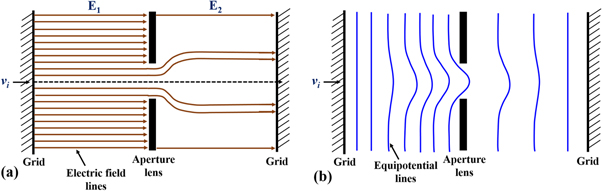
Figure 1. Schematic showing (a) electric field and (b) equipotential lines around the electrode having field E1 and E2 on both sides.
Download figure:
Standard image High-resolution imageFocused ion beams have become an important tool in today's science and technology for applications such as patterning [3–6], modification of surface properties [7, 8], milling [9, 10], implantation [11, 12], high resolution imaging [13], including studies of optical and field emission properties of created nano-structures [14, 15]. To address these applications, there are different types of ion sources, which are developed worldwide. Conventionally, liquid metal ion source (LMIS) based FIB is used, which can meet the demands of fabrication at high resolution (∼10 nm) [16]. However, this is faced with some limitations such as : (i) primarily gallium (Ga) ions are employed, which introduces metallic contamination to the target sample, (ii) it provides a small beam current (∼1 pA–10 nA) and therefore leads to slow volume milling (e.g. to mill out 25 × 104 μm3 volume of Si with a milling rate of 2.7 μm3 s−1, a 30 keV/10 nA Ga ion beam requires more than 24 h) [17, 18].
To overcome these limitations, plasma based ion sources are being developed worldwide [18–22]. Notable plasma ion sources are Penning ion sources, filament driven plasma ion sources, RF driven ion sources, and microwave plasma ion sources. Penning ion sources have high current density, but discharge instability and low efficiency are major issues, whereas filament driven ion sources are known to have lower current density and smaller lifetimes due to wear and tear of filaments [20, 23]. The RF driven ion sources have higher current density and smaller energy spread, however the main issue here is instability, due to switching from capacitively coupled mode to inductively coupled mode [20]. Therefore, microwave plasma based ion source is developed, which provides a stable high density plasma and high current density beams without such limitations [24]. The beam brightness, current density, ion energy spread are figures of merit of a FIB system which tell about the quality of the beam, these parameters are mentioned in details in section 3. The advantages of using plasma as ion source are : (i) variable ion beam species (He, Ar, Kr, Ne, Xe, etc) can be obtained, (ii) has the capability to provide large beam currents (∼1 pA–10 μA), and therefore can result in rapid volume milling without metallic contamination [24–27]. Plasma based ion sources can be easily used to treat semiconductors, and biomaterials by employing inert gas ions. Different types of plasma and other ion sources are mentioned below in details in section 2.
Some reported commercial FIBs are Ga FIB (FEI Nova 600 NanoLab DualBeam) which is a LMIS FIB, among the plasma based FIBs are the Xenon FIB (TESCAN) [28, 29], i-FIB, Helios NanoLab PFIB DualBeam, and Helium ion microscope (model Zeiss Orion) [30]. Advantages and limitation of Ga FIB are well known and mentioned above. The commercially available Xenon PFIB (by TESCAN USA Inc.) is a Xe inductively coupled RF plasma ion source based FIB which has benefits that Xe implants less in comparison to Ga atoms due to its inertness, and sample's electrical behaviour remains unchanged [28, 29]. This implies that Xe plasma FIB does not change sample amorphization or phase significantly even at 30 keV and 60 nA current. i-FIB is another commercially available FIB which is 50 times faster than the Ga FIB and can provide different ion species such as Xe+, Ar+, N2 + and He+. Helios NanoLab PFIB DualBeam is a dual beam system which uses Xe plasma as an ion source and can also be used for high resolution imaging in both 2D and 3D. However, all the above plasma FIB systems, use largely RF plasma technology and can have its own limitations as mentioned earlier and elaborated in a later section, in terms of beam stability. Helium ion microscope (ORION, Carl Zeiss) is a gas field ion source (GFIS) based FIB and it is used for very small scale fabrication with 2 times smaller damage than the conventional Ga FIB [31]. The present research discusses a microwave plasma based FIB which is not currently commercially available, and to the best of our knowledge has been pioneered in our laboratory at IIT Kanpur [24, 32].
Besides, employing electrostatic lenses, for further reduction of focused beam size, the source size (plasma electrode aperture) can be reduced for a constant demagnification of the lens. Additionally, micro-glass capillaries can be employed to reduce the source size which guides the ion beam without significant loss of beam current, which is crucial. It is found that during beam transmission, incoming ions get deposited on the capillary inner wall which further guides the ions towards the capillary axis due to repulsive force and maintains the initial charge state of ions [33–39]. An enhancement in current density at the focal point (FP) is also observed which may provide higher milling rate at the target sample [39].
Knowledge of FP is important for fabrication of samples, because beam current density is maximum at focal point and the beam size is minimum [25, 26]. Therefore, the samples need to be kept at the FP for rapid processing with highest resolution. In optics, FP is determined from the information of lens's geometry and material property. However, in plasma based FIBs, the determination of FP is challenging and depends on plasma parameters such as space potential, initial kinetic energy related to the Bohm velocity, ion current density, electron and ion temperature, ion mass, and beam parameters such as beam energy, geometry of the lenses, plasma electrode and beam limiter aperture sizes, and potential applied to the lenses [26].
The present article provides a tutorial of the different aspects of the state of the art and a review of recent research results on high aspect ratio micro structuring of materials using a microwave plasma (MWP) based focused ion beam system developed in our laboratory. Further, the guiding capability of a micro-glass capillary which can be important for reducing the beam source size without significant loss in beam current, is demonstrated. The variation of beam size and demagnification factor with plasma electrode (PLE) aperture size is presented, where enhanced nonlinear demagnification is observed when the aperture size of PLE is reduced to below the Debye length. Additionally, submicron focusing of plasma ion beams is also presented which is a new achievement in MWP based focused ion beam systems.
2. Ion sources for FIB applications
2.1. Gas field ion source
In gas field ion sources (GFIS), ions are generated by field ionization on expose of gas to a high voltage ∼1010 V m−1 with the help of a needle tip of tungsten having end radius ∼20–100 nm [16, 40–43]. Ion are extracted through an aperture of 0.5 mm. However, GFIS have some limitation such as: (i) tip has to be maintained at cryogenic temperature <77 K (ii) provides small beam current (∼0.1–10 pA) and (iii) therefore, leads to slow volume milling.
2.2. Liquid metal ion source
Liquid metal ion sources (LMIS) use a tungsten needle and liquid metal slowly come to end (tip) of the needle by capillary action, and a high voltage is applied to the extractor in the range ∼2–10 kV [16]. Due to balance between surface tension force and electrostatic (extraction) force, a conical shape 'Taylor cone' is formed at the tip, and ions come out from the tip due to field ionization. Conventionally, Ga based focused ion beams (FIB) are employed which has a few limitations such as : (i) primarily Ga ions are employed due to its low melting point ∼30 °C (ii) Ga introduces metallic contamination to the substrate [44], which can be a disadvantage in certain applications, and (iii) the beam current is small and lies in the range ∼1 pA–10 nA, therefore it takes long milling time to process the sample [17, 18].
2.3. Plasma based ion sources
Since plasma is a fourth state of matter and a collection of electrons, ions and neutral particles [45], ions can be extracted from matter in the plasma state. Plasmas are attractive because they can be also created of inert gaseous elements. Therefore, in order to overcome the above mentioned limitations, plasma based focused ion beams are being developed worldwide, which has the capability to address emerging research applications and can provide both non-toxic beams by the application of inert gaseous ions, and support rapid processing of materials due to availability of higher beam currents [18–22]. Currently, plasma ion beam processing is becoming increasingly important for processing biomaterials with applications in artificial heart valves and orthopedic prostheses [46]. Moreover, employing a variety of ion beams of different masses leads to controllability of the momentum transferred to the substrate and one can create structures with widely varying aspect ratios. There are different types of plasma ion sources which are briefly mentioned below.
2.3.1. Penning ion source
In penning ion source, plasma is created using a cold cathode and high voltage. The electrons oscillates between cathode and anode to initiate the discharge and plasma is confined in a penning type geometry [47]. Thereafter, ions are extracted using an electrostatic lens system. The main advantages of this system are compact design and high current density. It has a few drawbacks such as discharge instability, metallic contamination to the target sample and low efficiency.
2.3.2. Filament driven ion source
In filament driven ion source, a hot filament is used to generate the plasma and confinement is achieved using a magnetic multicusp [22]. Here, the main advantages are its smaller energy spread, source controllability and universality. It has some disadvantages such as small filament lifetime which requires frequent maintenance, contamination by sputtered materials from the hot filament, low beam brightness (for high current applications), and cannot be used to create plasmas of several elements (except inert gases, H2, halogens and freons) as it may lead to filament corrosion.
2.3.3. RF driven ion source
RF plasma ion sources are generated by the absorbed RF energy which creates the discharge. There are two type of RF ion sources namely: (i) inductively coupled and (ii) capacitively coupled. Jiang et al [20, 44] have developed a RF driven multicusp plasma, operated on inductively coupled discharge mode for FIB applications. Further Smith et al [18] and Nabhiraj et al [21] have separately developed RF ion sources for the FIB system. These can provide good current density and small energy spread. Smith et al have shown reduced brightness 5.4–9.1 × 10³ Am−2 sr−1 V−1 and energy spread 10–7 eV for argon and xenon respectively and Nabhiraj et al have produced argon ion beams with energy spread of less than 5 eV and brightness of 7100 Am−2 sr−1 eV−1. However, RF ion sources suffer from limitations such as power coupling issue, reduction of source life time, jumping of capacitively coupled mode to inductively coupled mode, while changing input power or gas pressure, which therefore can affect the beam extraction and milling performance.
2.3.4. Microwave plasma ion source
In microwave plasma ion sources, plasma is created using microwave energy. The seed electrons absorb the microwave energy and energy of electron increases due to elastic collision with neutral, and ionization occur with the inelastic collisions [48, 49]. Plasma confinement is brought about by employing magnetic multicusp, where magnetic mirror effect [45] takes place to obtain a central dense plasma.
Microwave plasmas have several advantages over other ion sources such as sputtering and contamination are minimum because MW plasma does not need any electrode or filament to create plasma. Other advantages are: (i) clean and contamination free plasma (ii) possibility of obtaining variable ion beam species, (iii) large focused beam current, (iv) un-magnetized beam extraction region, (v) long life time and requires less maintenance, and (vi) small ion energy spread near the plasma meniscus from where the ion are extracted [50].
Other ion source such as Cs+ low temperature ion source (LoTIS) is still in the process of development which has a projected sub-nanometer beam spot size at 1 pA and a maximum current of several nanoamps [51]. It has the application in the area of integrated secondary ion mass spectrometry.
A detailed comparative analysis of different types of ion sources are presented in table 1 below.
Table 1. Source and beam parameters of different types of ion sources [16, 18, 21, 47, 52].
| Ion sources | Reduced brightness (Am−2 sr−1 V−1) | Ion energy spread (eV) | Beam current |
|---|---|---|---|
| GFIS | 1 × 10⁹ | 1 | 0.1 pA to 10 pA |
| LMIS | 1 × 10⁶ | 5 | 0.2 pA to 20 nA |
| Penning | 1 × 10⁵ | 3 | 0.7 nA to 5 nA |
| ICP | 4 × 10²–1 × 10⁴ | 3.5–5 | 0.1 pA to 10 μA |
| MWP | 1 × 10⁵ | 5 | 5 pA to 10 μA |
| LoTIS | 2 × 10⁷ | 0.34 | 0.5 pA to >1 nA |
Some other reported ion sources are laser ion sources [53], electron impact gas ion source [54], and electron beam ion sources and traps [55, 56]. In laser ion source, laser is used to create plasma and it is proposed that it can be used to produce ions of both gas and metals with energy spread <0.1 eV. In electron impact gas ion source, electron beam is used to create ions by ionizing the gas atoms or molecules. Here, reduced brightness was reported to be 102 Am−2 sr−1 V−1 with less ideal experimental conditions and the proposed brightness is 104 Am−2 sr−1 V−1. In electron beam ion sources and traps (EBIS/EBIT) at Lawrence Livermore National Laboratory (LLNL) USA, self cooled ions can be obtained from EBIS/EBIT and this self cooling mechanism can enable the development of a high brightness source [42]. Recently, a transformer coupled plasma (TCP) ion source has been reported which has the capability to provide light (H, He) and heavy ions (Kr, Ar) both with small beam emittance ∼0.2 ( mm mrad) and high beam current 0.55 mA [57]. Other reported ion sources are anode spot plasma ion source [58], mass filtered plasma focused ion beam [59], Liquid Metal Alloy Ion Sources (LMAIS) [60] which of course belong to the category of LMIS, and ECR ion source (ECRIS) [47].
3. Figures of merit
3.1. Ion energy spread
Ion energy spread ( ) is an important parameter to tell about quality of the beam. Spread in ion energy is the reason of chromatic aberrations in ion beam optics. If
  is small then almost mono-energetic beam is obtained at the target sample.
  is measured at the extraction region of multicusp using an ion energy analyser (IEA) probe [50] and it is found to be small ∼5 eV which is comparable to conventional LMIS based FIB [61]. Figure 2 shows the ion energy distribution (IED) obtained from IEA probe where it is compared with Maxwellian (fM) and Druyvesteyn (fD) energy distribution having same mean energy. It is observed that low energy and high energy tail ions are absent in IED and almost mono-energetic beam with energy spread ∼5 eV is obtained [50].
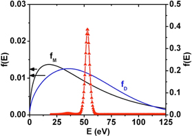
Figure 2. Comparison of ion energy distribution at the plasma meniscus with Maxwellian and Druyvesteyn energy distribution of same mean energy. Reprinted from [50], with the permission of AIP Publishing.
Download figure:
Standard image High-resolution image3.2. Focused beam current
Focused beam current is another parameter which tells about current density at the target sample. It also gives an idea about milling time i.e. sample processing time is less for larger current. Beam current in microwave plasma based MEFIB system is measured using a Faraday cup and it is found to be in the range ∼5 pA–10 μA [25] which is much larger and has significantly wide range in comparison to the conventional Ga FIB (∼1 pA–10 nA) [17, 18].
3.3. Beam emittance and brightness
Beam emittance is another figure of merit of the beam and it represents the optical performance of the beam which is the product of beam width and transverse velocity spread [62]. Beam emittance is represented more appropriately as normalized beam emittance as,

where,  is the root mean square (rms) beam width and
  is the transverse velocity spread respectively, Ti
: ion temperature, rs
: beam radius, Mi
: ion mass, and c: speed of light.
is the transverse velocity spread respectively, Ti
: ion temperature, rs
: beam radius, Mi
: ion mass, and c: speed of light.
Whereas a better figure of merit of the beam is brightness of the beam which is given as the ratio of beam current (IC
) to  for an axisymmetric beam. Beam brightness is given as [62],

and since ε is found to change with beam energy, therefore the normalized beam brightness Bn is defined as [62],

where, Js is the source current density. The above equation (3) is for beam brightness at source side. The image side brightness is given by [62],

where, Ji
is the current density at the image side. dΩ is the beam solid angle given as  where
where  is the beam divergence and D is the beam diameter at the image.
The estimated reduced source side brightness for the MEFIB ( where
where  is the current density at PLE aperture,
  is the ion temperature) for 1 mm plasma electrode (PLE) aperture size and
  ∼0.2 eV, is found to be ∼1 × 10⁵ Am−2 sr−1 V−1, which is close to the LMIS based FIB [22].
3.4. Aberrations
In beam optics aberrations are found in a similar manner as in geometrical optics and parallel beams are focused at different points, which arise from (i) spherical and (ii) chromatic aberrations. Spherical aberrations occurr due to radial variation of the focusing electric field, and ions at different radial positions are focused at different positions of beam axis. The narrowest beam size i.e. diameter of the circle of least confusion defined as spherical aberration, is given by [63–65],

where,  is a dimensionless constant and found to lie in the range 2–10 for Einzel lenses,
  is a scaling parameter which is related to the axial extent of the field,
  is the beam radius at the entrance.
  is calculated for the MEFIB lens and it is found to be ∼0.008 μm where
 and
and  are taken as 10 (for decal-accel Einzel lens), 5.17 cm and 130 μm respectively.
Whereas, chromatic aberration occurr due to spread in ion energy of the beam because  is higher for ion beam energy
  than for ions having energy
  The diameter of the circle of least confusion for chromatic aberration is given by [63–65],

where,  is a dimensionless factor which lies in the range 1–5 for Einzel lenses.
  is calculated for the MEFIB and it is found to be 0.125 μm where
 and
and  are taken as 5 (decel-accel), 26 keV and 5 eV [50] respectively.
Therefore it is observed that chromatic aberration is the main reason of aberrations in ion beam optics of MEIB. The estimated maximum deviation in the focal length ( ) has been found to be ∼4.5% [26].
Figure 3 shows a comparison of different ion sources for FIB applications based on figure of merit, Brs/ E2 (Brs is the reduced source brightness and
  E is the ion energy spread) and focused current density [23, 66]. The performance of microwave plasma (MWP) ion source is better than conventional LMIS in terms of focused current density which can further be improved by reducing the beam size. The figure of merit, Brs/
 E2 of MWP ion source is comparable to other ion sources, however it has several other advantages as mentioned above and will be further elaborated in the later sections.
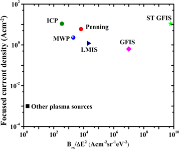
Figure 3. Focused current density with figure of merit, Brs/ E2 for different ion sources. ICP: inductively coupled plasma [18], MWP: microwave plasma, LMIS: liquid metal ion source, GFIS: gas field ion source, ST GFIS: GFIS with cryogenically cooled supertip [23, 66]. Reproduced from [23] Guharay S K, Sokolovsky E, and Orloff J 1999 Characteristics of ion beams from a Penning source for focused ion beam applications J. Vac. Sci. Technol. B 17, 277], with the permission of the American Vacuum Society.
Download figure:
Standard image High-resolution imageTo address some of the issues faced by other ion sources and meet the requirements of emerging applications, a microwave plasma based multi-element focused ion beam (MEFIB) system has been developed [24, 25, 27, 35, 36, 67–71] . The system provides variable projectile masses by employing different gaseous plasma ions and higher beam currents can be obtained. A detailed study of MEFIB system is presented in section 4.
4. Multi-element focused ion beam system
The multi-element focused ion beam system has provided focused ion beams of various ion beam species such as Ar, Kr, Ne, H2 with controllable beam current in the range 5 pA–10 μA and beam energy up to 30 keV, without introducing metallic contamination on the substrate. A distinct advantage of the MEFIB is that the beam size can be varied in the range from submicrometer to ∼25 μm, thus widely tunable milling rates in the range 1–500 μm3 s−1 are realized [24, 25, 27, 35, 36, 67–71]. Micropores (∼30 μm diameter) on 11 μm thick aluminium foils have been created with a milling rate of ∼300 μm3 s−1 [68]. The experimental setup is discussed, and plasma creation, confinement and beam extraction are presented in detail in the next section.
4.1. Experimental setup
The experimental system has mainly four parts which are: (i) plasma column, (ii) beam column, (iii) experimental chamber, and (iv) stage manipulator as shown in figure 4(a) [24, 25, 27]. In plasma column, microwaves of frequency 2.45 GHz is launched into a vacuum chamber (∼10−7 Torr) and a high-density plasma is formed, which is confined using an octupole magnetic multicusp [25]. The plasma density in the central region of the multicusp (∼r = 2–2.5 cm) is overdense for the input wave frequency (∼1011 cm−3). The cut-off density is 7.44 × 1010 cm−3 for EM waves of frequency 2.45 GHz. The working pressure of the neutral gas is maintained at ∼0.25 mTorr. Typical ion and electron temperatures are ∼0.2 eV [69] and 10 eV respectively, and the plasma frequency is ∼2.83 GHz [26]. It is noted that the plasma frequency is slightly higher than the wave frequency. Wave propagation through a bounded overdense plasma has been earlier demonstrated [72]. The beam column has many electrodes which are used to extract and focus the ion beam. The first electrode which faces the plasma is called plasma electrode (PLE), and at PLE a plasma sheath is formed which further helps to extract the ions. The sheath accelerates the surrounding ions toward the PLE wall and ions emerge out through the aperture. Thereafter, decel-accel type Einzel lens [26] EL1 is used to further extract and accelerate the ions towards the lens axis, the beam limiter (BL) trims the beam and finally EL2 provides the required focusing field and energy to the beam [25]. In the experimental chamber, several experiments are performed such as beam current measurement and beam writing. Microstructures are created by moving the sample in X and Y directions, and the sample is positioned along the beam direction (Z-axis) using a XYZθ stage manipulator.
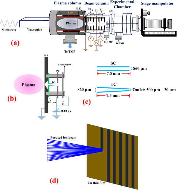
Figure 4. Schematic diagram of (a) MEFIB experimental setup, PLE: plasma electrode, MC: muticusp, TMP: turbo molecular pump, EL1 and EL2: Einzel lenses, SH: sample holder, BL: beam limiter, GV: gate valve, V1, VS and V2: negative high voltages applied to the lenses. Reprinted from [26], with the permission of AIP Publishing. (b) Capillary guiding experimental setup, PE: puller electrode, C: collector, TC: tapered capillary (c) straight (SC) and tapered capillaries (TC). Reproduced from [39]. © IOP Publishing Ltd. All rights reserved. (d) Schematic of focused ion beam showing beam writing on Cu thin film.
Download figure:
Standard image High-resolution imageFor capillary guiding experiment, the beam column of the MEFIB is replaced with the capillary experimental setup as shown in figure 4(b) [26, 39]. In beam column, a plasma electrode (PLE) having central aperture 500 μm, a puller electrode (PE) and collector (C) are employed. A straight (SC) or tapered capillary (TC) of inlet ID 860 μm and variable outlet ID 860 μm–20 μm is attached to the PLE using a Perspex holder. To extract the ions, a PE of central aperture 1.5 mm is kept 8 mm away from PLE. C is kept at a gap of 6 mm from PE to measure the transmitted beam current (figure 4(b)). Insulating (Teflon) spacers are used to maintain fixed distances between PLE, PE and C as mentioned above. PE and C are commonly connected to same negative high voltage which is varied in the range 0 to −10 kV and the PLE is grounded, therefore an accelerating beam is transmitted through the capillary with the increase in PE voltage [26].
Argon plasma is ignited at neutral gas pressure at 0.25 mTorr and the microwave power of 250 W as mentioned above. Plasma sheath is created on PLE and Ar ions hit the PLE with Bohm velocity ( where Te
is the electron temperature,
where Te
is the electron temperature,  is the Boltzmann constant, and Mi
is the mass of Ar ions) ∼4.9 × 10³ m s−1 for a
is the Boltzmann constant, and Mi
is the mass of Ar ions) ∼4.9 × 10³ m s−1 for a  ∼10 eV [36], and come out through the PLE aperture. Further, ions are accelerated by a negative voltage (V) applied to PE and simultaneously ion beam current (IC
) is measured at C using collector current measurement unit (Ionics Ltd, India). Figure 4(c) shows different capillaries that have been fabricated for experiments, of 860 μm inlet inner diameter (ID) and of varying outlet ID as 500 μm, 300 μm, 200 μm, 110 μm, 45 μm, and 20 μm. For measurement of beam size, the beam impression is obtained by irradiating the beam for 6 min on a sample comprising of 50 nm copper thin film, which is deposited on an aluminium foil and attached to PE.
∼10 eV [36], and come out through the PLE aperture. Further, ions are accelerated by a negative voltage (V) applied to PE and simultaneously ion beam current (IC
) is measured at C using collector current measurement unit (Ionics Ltd, India). Figure 4(c) shows different capillaries that have been fabricated for experiments, of 860 μm inlet inner diameter (ID) and of varying outlet ID as 500 μm, 300 μm, 200 μm, 110 μm, 45 μm, and 20 μm. For measurement of beam size, the beam impression is obtained by irradiating the beam for 6 min on a sample comprising of 50 nm copper thin film, which is deposited on an aluminium foil and attached to PE.
4.2. Mechanism of plasma generation, extraction and focusing of ion beams
An overview of plasma generation and sustenance of the plasma in the multicusp magnetic field of the ion source is presented. It is observed that initially launched electromagnetic (EM) waves are not permitted to freely pass through the circular plasma chamber because the dimension of the chamber (referred here as a waveguide having radius R = 3.5 cm) is smaller than the cut-off radius (Rc = 3.6 cm) for the fundamental TE11 mode of frequency 2.45 GHz. However, initially at the waveguide entrance, gaseous breakdown occurs due to an evanescent wave and a plasma is formed [24]. The refractive index of the medium at the entrance varies radially with the plasma density. After the formation of the plasma at the entrance of the circular chamber, EM waves can propagate though the waveguide in the peripheral regions, where the plasma density is lower and the wavelength is reduced because of the collisionally broadened upper hybrid resonance region [24]. The propagation of the EM waves is possible when λ∕λc < 1, where λ is the microwave wavelength in the magnetized plasma region and λc is the cut-off wavelength in the waveguide without any plasma [24]. It is demonstrated that at lower pressures near the peripheral plasma, the incident microwaves can propagate through the small annular windows [24]. Moreover, it has been later shown that in the presence of a magnetic field for waves launched in the k ⊥ B mode, wave propagation through a central overdense plasma is significant when the cross-sectional size of the conducting boundary of the plasma is decreased [70]. Electron cyclotron (ECR) and upper hybrid resonances (UHR) take place near the wall of the multicusp and these are the active particle generation regions. The charge particles diffuse towards the central region of the waveguide and is radially confined by the multicusp magnetic field [73]. Larmor radius of the charged particles decreases as the particles move towards the wall of the multicusp, due to increase in the magnetic field, and particles get reflected to the central region due to magnetic mirror effect. The particle loss percentage is estimated to be about 1% through the loss cones of the multicusp [74]. End plugging of the multicusp prevents axial diffusion of the particles, which is realized by reversing the polarity of the end magnets at the two ends of the multicusp [75] and in this way, a high-density plasma is confined along the axial length of the multicusp. Typically, the plasma density is found to lie in the range 1010–1011 cm−3, and electron temperature in the range 5–20 eV which is lower at the centre of the multicusp and higher near the peripheral region where resonances occur. An almost monoenergetic (Δ E ∼ 5 eV) ion beam is extracted from the central uniform high density plasma [50].
The mechanism of beam extraction and focusing is summarized below. Ions arrive from the bulk plasma to the sheath edge of PLE with the Bohm velocity vb
(=  ) [76]. The ions then get accelerated toward the PLE aperture from the sheath edge because of the negative potential of the PLE wall (with respect to the bulk plasma) and attain a velocity vi
, which is given by
) [76]. The ions then get accelerated toward the PLE aperture from the sheath edge because of the negative potential of the PLE wall (with respect to the bulk plasma) and attain a velocity vi
, which is given by  where
where  is the wall potential of PLE. The reference is the plasma potential which is taken as zero. Further, the incoming ions from the PLE aperture are accelerated by the EL1 voltage to a velocity
  given by,

where,  is the voltage applied to EL1. Since EL1 is an accel-decel (Einzel) lens, the ions emerge out of EL1 with velocity
  The ions then get accelerated by the voltage applied to the BL aperture and come out from it with a velocity
  given by,

where,  is the voltage applied to BL. Thereafter, the ions are further accelerated by the second set of Einzel lens EL2, and finally attain a velocity
  given by,

where,  is the applied voltage to EL2. This is the final velocity with which ions come out from the lens and hit the target sample. From equation (9), it is seen that the final velocity of ions depends only upon
  and is independent of the intermediate voltages applied to the other electrodes (EL1 and BL). The off axial ions are pulled toward the centre by the focusing field, which finally focuses the beam with beam energy ∼
 Equation (9) is employed to calculate the total momentum transferred from the beam to the target sample in section 3.1.
Figure 5 shows the equipotential lines in the neighbourhood of each electrode, which are curved and behave like optical lenses (which focuses the optical rays) for the incoming beam. The beam is extracted, accelerated and focused due to applied electric fields, where ion beams are guided along the perpendicular direction to the developed equipotential lines in the electrostatic lens system [26].

Figure 5. AXCEL-INP simulation shows equipotential lines near the electrode aperture, similar to convex type electrostatic lenses for focusing of the ion beam. Reprinted from [26], with the permission of AIP Publishing.
Download figure:
Standard image High-resolution image5. Experimental results and discussion
5.1. High aspect ratio microstructuring and momentum transferred from the ion beams
Beam current is measured for different gaseous plasma ion beams (Ar, Kr, Ne and H2) for a 31 μm PLE aperture using a Faraday cup (National Electrostatics Corporation, USA). Beam current is extracted through micro apertures whose sizes are reduced to even smaller than the Debye length of the plasma. The Debye length is a plasma length scale below which external electrical disturbances are shielded off and is given by [25],

where 
 Te
and ne
are free space permittivity, Boltzmann's constant, electron temperature and electron density respectively. The PLE apertures of size 31 μm, 40 μm and 45 μm are employed in the experiments which are well below the typical Debye length of the plasma (∼100 μm for a density of 1.15 × 1011 cm−3 and a temperature of 10 eV). Therefore, neither the plasma meniscus nor plasma-sheath interface bends near PLE aperture nor plasma leaks through the aperture and a highly directional beam is obtained [77].
Te
and ne
are free space permittivity, Boltzmann's constant, electron temperature and electron density respectively. The PLE apertures of size 31 μm, 40 μm and 45 μm are employed in the experiments which are well below the typical Debye length of the plasma (∼100 μm for a density of 1.15 × 1011 cm−3 and a temperature of 10 eV). Therefore, neither the plasma meniscus nor plasma-sheath interface bends near PLE aperture nor plasma leaks through the aperture and a highly directional beam is obtained [77].
Figure 6(a) shows that beam current increases with EL1 voltage and tends to saturate after ∼1.5 kV. The observed trend is found to be similar for ion beams of each species (H2, Ne, Ar, Kr). From the saturation region, maximum value of IC
is plotted with ion mass ( ), which shows that as expected, IC
is inversely proportional to the square root of ion mass (
), which shows that as expected, IC
is inversely proportional to the square root of ion mass ( ) as shown in figure 6(b) [25, 27]. The error in the beam current measurement is very small ∼0.026 nA, which lies within the width of the symbols (figures 6(a) and (b)), and is not discernable. The beam current is measured for different EL2 voltages (V2) and values of saturated beam currents are found to be more or less similar and independent of V2. Further, stability of the extracted ion beam current with time is investigated using a high precision current measurement unit (Keithley picoammeter, model 6485) at different values of EL2 voltage in the range 18–30 kV as shown in figure 7. It is found that the beam is stable with time with a very small deviation ∼0.026 nA.

Figure 6. (a) Variation of beam current with extraction voltage V1 for the 31 μm PLE aperture size. (b) Variation of obtained maximum beam current with ion mass. Reprinted from [25], with the permission of AIP Publishing.
Download figure:
Standard image High-resolution image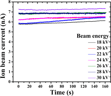
Figure 7. Beam stability result: variation of ion beam current measurement with time at EL1 = −2.2 kV and different beam energy (EL2 voltage) for 40 μm PLE aperture size.
Download figure:
Standard image High-resolution imageFor future applications of the beam, the sample to be processed needs to be kept at the focal point (FP). It has been found that precise determination of FP is difficult by simply creating and measuring the circular beam spots along the beam axis (Z-axis), because of over irradiation of the beam which makes accurate measurement of beam spot radius difficult near the FP [25, 78, 79]. Therefore, a method involving minimum irradiation time is considered for FP determination, because beam current density is highest at FP and the beam can create a spot in minimum time [25]. In order to experiment this, beam writing is carried out as shown schematically in figure 4(d), by moving the sample in X and/or Y direction with different writing speeds in the range 1.5–15 μm s−1 and by placing the sample at different axial (Z) positions. Computer controlled LAB-VIEW program is used to move the sample in X and Y directions with the help of XYZ
 stage manipulator where X and Y directions are perpendicular to the beam and Z is along the beam axis. The created beam impressions (lines) are analysed under the optical microscope and minimum irradiation time is calculated using
  where
where  is the line width of the created line at maximum writing speed
  for creating a clear line. The line width
  is measured using ImageJ software [80]. From figure 8, FP is found to be 6.7 mm away from the last electrode of EL2 for 40 μm PLE and 26 keV beam energy. FP is determined for different PLE aperture sizes and beam energies, and while performing experiments, the samples are kept at the determined focal point.
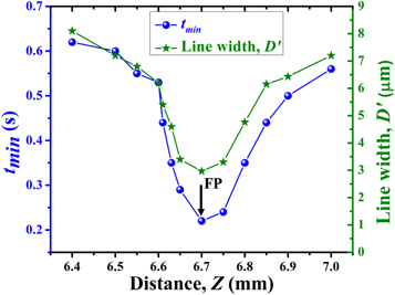
Figure 8. Determination of focal point considering tmin for 40 μm PLE aperture at EL1 = 2.2 kV, EL2 = 26 kV and BL = 17.3 kV. Variation of minimum irradiation time (tmin) and line width (D') with distance from the last electrode of EL2, obtained at highest beam writing speed. Reprinted from [25], with the permission of AIP Publishing.
Download figure:
Standard image High-resolution imageThen sample is kept at FP and beam writing is performed for 40 μm PLE aperture. Lines are created on Cu thin films of thickness ∼150 nm, for different writing speeds (dwell time) using 26 keV, Ne, Ar and Kr ion beams. The aspect ratio ar (line width/depth) of the created lines is calculated and it is found that variable high aspect ratios in the range ∼100–1000 are realized in the created structures as shown in figure 9(a) [25]. For Ar ion beams, distinct lines are obtained at higher writing speed, because Ar has a combination of beam current and ion mass such that the mass is not as small as that of Ne ions nor the obtained current is as low as that for Kr ions. ar is found to be higher for Ne ion beams because Ne has higher beam current (∼20 nA) and therefore higher line width due to self-coulomb repulsion and smaller line depth because of lower ion mass are realized. Grating like microstructures are created on 50 nm Cu thin film employing 26 keV Ne, Ar and Kr ion beams for 40 μm PLE as shown in figures 9(b)–(d) [25]. To calculate the impact of the beam on the target sample and to determine the efficacy of beam processing, a parameter called 'current normalized force (CNF)' which is the total momentum transferred per unit time, normalized with the beam current, given by [25], Reproduced from [Maurya S K, Paul S, Shah J K, Chatterjee S, and Bhattacharjee S 2017 Momentum transfer using variable gaseous plasma ion beams and creation of high aspect ratio microstructures J. Appl. Phys. 121 123302], with the permission of AIP Publishing.

where, p, N,  t and I are transferred momentum, number of ions and ion mass, beam irradiation time and beam current respectively and
  is the maximum beam angle at FP, is defined.
  is determined from equation (9). Detailed calculation of CNF can be found in [25].
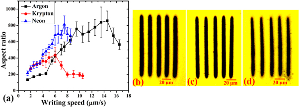
Figure 9. (a) Variation of aspect ratio with writing speed for Ne, Ar and Kr ion beams . (b)–(d) Optical microscopy images of grating like microstructure, created using 26 keV Ar, Kr and Ne plasma ion beams respectively. Reprinted from [25], with the permission of AIP Publishing.
Download figure:
Standard image High-resolution imageThe beam size can be further reduced by employing capillary at the exit of the PLE, this reduces the beam source size and enhances the demagnification of the lens. Therefore, micro-glass capillary guiding is demonstrated below for different smaller capillary outlet IDs.
5.2. Capillary guiding of ion beams: charge dissipation and self focusing
The ion beam guiding capability of insulator capillaries has become a subject of interest [33–39, 81–88] after the first observation of keV ion beam guiding through nano-capillaries by Stolterfoht et al [33]. In the early work [33], it is reported that the capillary inner wall gets charged while beam transmission and the initial charge state of the ions are maintained throughout the capillary. This guiding capability offers an unique opportunity to manipulate the beam by varying the capillary geometry (outlet inner diameter size). The beam guiding capability is also investigated by tilting the capillary up to tilt angle ±100 mrad and maintaining the initial charge state [34]. Capillaries of tapered geometry have been used to generate microbeam [34] and nanobeam [81, 82]. There are reports of ion beam guiding through a curved capillary [83, 84] which may be used as a beam bender like optical fibre. Charged particle guiding has applications such as beam steering [85], focused charge particle beams [38, 86], including biological applications such as irradiation of single living cells [87].
Therefore, to further reduce the final beam size of MEFIB, micro-glass capillary can be employed to reduce the source size without significant loss in beam current. Before implementation, guiding capability of plasma ion beam through micro-glass capillary is investigated. The experimental details are mentioned in section 4.1. Current density at the capillary outlet, which is a ratio of the beam current to the capillary outlet area, is measured for capillaries of different outlet inner diameters. Beam transmission is found to occur when the ion energy is greater than a certain threshold voltage as shown in figure 10(a). It is observed that the current density increases with decrease in capillary outlet ID because of loss less guiding of the ion beams, and a high current density is obtained ∼600 Am−2 for 20 μm capillary outlet ID [39]. It is found that the ratio of the outlet to inlet current density η > 1 for each capillary outlet ID employed in the experiments, i.e. guiding is efficient. The value of η is a measure of the guiding capability of the capillary for ion beams [35, 83, 88].

Figure 10. (a) Variation of beam current density with extraction voltage [39]. (b) Variation of deflection angle of the beam with the tilt angle of the capillary. Inset shows beam spots for tilt angles −5° to +5° (left to right) in step of 2.5° for 200 μm capillary outlet ID. Reproduced from [39]. © IOP Publishing Ltd. All rights reserved.
Download figure:
Standard image High-resolution imageDirectional guiding capability of the capillary is also demonstrated by tilting the capillary of outlet ID 200 μm [39]. Capillary is tilted from −5° to +5° in step of 2.5° relative to incident beam direction and beam spots are created on Cu thin film deposited on Al foil substrate by maintaining the extraction voltage at 10 kV. The step size is chosen as 2.5° because a small capillary of length 7.5 mm and outlet inner diameter (ID) 200 μm is employed and the sample is kept maintaining a gap of ∼0.5 mm from the capillary outlet. Therefore, for a smaller step size of tilt angle (∼1°), the vertical distance of shifted beam spot is only ∼136 μm from the center of beam axis. Hence, beam spots for tilt angles of ∼1° may overlap at these small angular step sizes for the 200 μm capillary outlet ID. Moreover, when we tilt the capillary with an angle  the ion beams hit the target sample with an angle (90−
 ), which results in elliptical spot size and may artificially increase the beam spot size. Therefore a step size of 2.5° was chosen to avoid spot size overlapping.
Variation of beam deflection angle with capillary tilt angle is shown in figure 10(b), which demonstrates that beam is guided well along the tilt direction of the capillary [39]. Therefore, capillary guiding of the beam is found to be efficient. Beam spots for different tilt angle is shown in the inset of figure 10(b).
Hysteresis in beam current with extraction voltage (ion energy) is observed as shown in figure 11(a) and the mechanism of hysteresis is explained below [34, 35, 39]. While increasing the extraction voltage V, charges start to accumulate on the inner wall of the capillary and a retarding potential barrier develops and therefore beam transmission through the capillary is difficult and beam current is negligible until about 8 kV. When ion energy becomes greater than the retarding potential barrier, most of the deposited charges diffuse to the electrode and a sudden increase in beam current is observed; this particular extraction voltage is called 'upper threshold voltage'. While decreasing V, beam current is obtained up to 2 kV because retarding potential barrier has decreased due to diffusion of deposited charges, and therefore hysteresis is observed due to dissipation of charges [39]. The sharp decrease in current occurs at a particular voltage called 'lower threshold voltage'. Dissipated charge is calculated from the hysteresis area by dividing the area into n vertical strips of width ΔV and heights Ik↑ and Ik↓ , where Ik↑ and Ik↓ denote beam current while increasing and decreasing V for kth strip, and is found to be [39],

where, Δt is the time taken to increase the extraction voltage by ΔV, Pd is the dissipated power which is the hysteresis area. The dissipated charge Q is calculated from equation (12) for different capillary outlet IDs as shown in figure 11(b) and it is observed that the dissipated charge is maximum for 300 μm capillary outlet inner diameter, because of higher hysteresis area which is a combined effect of higher beam current and large difference in lower and upper threshold voltages.

Figure 11. (a) Variation of ion beam current with extraction voltage [39]. (b) Dissipated charge for capillaries of different outlet IDs. Reproduced from [39]. © IOP Publishing Ltd. All rights reserved.
Download figure:
Standard image High-resolution imageFurther, created beam spots on Cu thin film (thickness ∼50 nm) deposited on Al foil substrate for different capillary outlet ID, are analysed under optical microscope (Carl Zeiss, AXIO imager.A1m). Variation of beam size (experimental and theoretical) with capillary outlet ID is investigated and shown in figure 12(a), it is found that the spot size decreases with decrease in outlet ID. The theoretical beam spot size is calculated from the knowledge of theoretical self focusing factor F (calculated below using PIC simulation) and capillary outlet ID  Experimental spot size (
 ) is fitted with a nonlinear equation as shown below [39],

where,  is the capillary outlet ID and it is a variable here, a = 140.92 μm and
  = 8.39 are constants and
  is the maximum value of
  i.e. inlet ID of the capillary ∼860 μm.
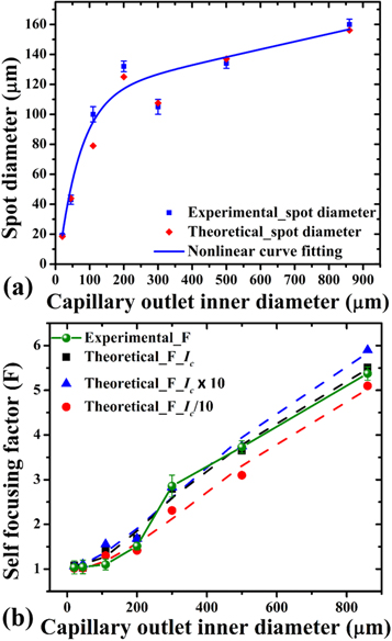
Figure 12. (a) Variation of spot diameter (experimental and theoretical approximated) with capillary outlet ID. (b) self focusing factor for different outlet ID for experimental beam current and assumed 10 times higher and lower beam current in the simulation. Reproduced from [39]. © IOP Publishing Ltd. All rights reserved.
Download figure:
Standard image High-resolution imageA self focusing of the beam inside the capillary is observed i.e. spot size is obtained to be smaller than the outlet ID of the capillary, and maximum compression of beam obtained is ∼81% for 860 μm capillary outlet. Therefore, a parameter called self focusing factor (F) is defined to investigate the self focusing effect and given as [39],

where, do and ds are capillary outlet ID and corresponding spot size respectively. When, do = ds and F = 1, unfocused parallel beam is expected. From figure 12(b), it is observed that F decreases linearly up to ∼300 μm capillary outlet ID, and then it is observed to vary nonlinearly with decrease in capillary outlet ID and finally tends to saturate for a capillary outlet ID of around 20 μm. For smaller capillary outlet, beam is compressed in a smaller region at the outlet, and therefore self-coulomb repulsion in the beam increases. The inward radial focusing force due to accumulated charges on the capillary wall is then unable to further compress the beam, therefore, F is found to decrease with decrease in capillary outlet ID and tends to unity for smaller outlet ID (20 μm) [39], which could indicate in the self-focusing limit.
Further, self focusing factor is calculated theoretically. There are three types of forces inside the capillary which guide the ion beam : (a) radially inward coulomb force due to accumulated charges on the capillary inner wall (b) radially outward self-coulomb repulsion force due to charges in the beam and (c) axial force  due to applied potential to the electrodes [39]. It is assumed that the current density
  flows in the z-direction and because of
  a magnetic field
  is generated in the
  direction. Therefore, a pinch force
  (Nm−3) on the ion beam acts in radially inward direction which compresses the beam and is calculated by ampere's law.
  force of a considered beam volume of length 100 μm near the capillary outlet is obtained as ∼2.6 × 10⁻²⁰ N, whereas resultant radial force
  on a single ion due to (i) accumulated charges on the wall and (ii) self-repulsion force in the beam, obtained from PIC simulation is ∼2.3 × 10⁻¹⁴ N which is in radially inward direction. Therefore,
  is significantly larger than the pinch force and in radially inward direction, therefore ions follow the trajectory inside the capillary due to resultant radial (
 ) and axial force (
 ) [39].
To calculate the self-focusing factor theoretically in terms of radial and axial force, spot radius and distance of the sample from the capillary outlet, it is assumed that beam gets self focused with an angle  during beam transmission as shown in figure 13. Here, L is the distance between sample and capillary outlet,
  and
and  are the measured beam spot radius and capillary outlet radius respectively. The self focusing factor is found as [39],

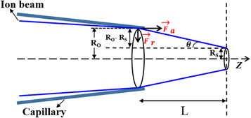
Figure 13. Schematic diagram showing self focusing of the beam inside capillary. Reproduced from [39]. © IOP Publishing Ltd. All rights reserved.
Download figure:
Standard image High-resolution image
F is calculated for different capillary outlet IDs (figure 12(b)) where values of  and
and  are taken from particle in cell (PIC) simulations, which is carried out as described below. Figure 12(b) shows that calculated F matches well with the experimental F and follows similar behaviour. F is also calculated by considering 10 times lower and higher beam current in the simulation and it is found that F is higher for higher current because of deposition of charges on the capillary inner wall and corresponding
  increases for larger beam current [39].
Particle in cell (PIC) simulation is carried out to understand the underlying physics of the capillary guiding of ion beam [34, 35, 39]. It self-consistently calculates the potential, electric field and ion trajectory for the input beam inside the capillary. The 2D simulation code developed in house, considers the azimuthal symmetry for parallel and collinear axis of the capillary and beam. The region of interest has been divided into 325 × 925 square grids of grid size 0.02 × 0.02 mm2 where grid parameter h is chosen to be 0.02 mm. The potential at each grid point (I, j) is calculated by solving Poisson's equation and using successive over relaxation method [89], where the over relaxation coefficient (w) is taken as 1.95 for fast convergence. Potential  at each grid point (I, j) for a charge density
  is given as,

where,  is the free space permittivity and equation (16) is solved until a stable solution is obtained.
PIC simulations are performed for different capillaries to investigate the self focusing and guiding of the beam. Figures 14(a)–(d) shows the charges distribution inside the capillary and figures 14(e)–(h) shows ion beam trajectory through the capillary, which clearly demonstrate the self focusing of the beam though the capillary. From figure 14, it is observed that self focusing decreases with decrease in the outlet ID and matches with experimental results as shown in figure 12(b) [39].

Figure 14. Simulation results showing the self focusing of the beam: (a)–(d) shows beam transmission (e)–(h) shows ion beam trajectory, through the tapered capillary of inlet ID 860 μm and outlet IDs 500 μm, 300 μm, 200 μm and 110 μm respectively. Reproduced from [39]. © IOP Publishing Ltd. All rights reserved.
Download figure:
Standard image High-resolution imageThe axial and radial fields obtained from the simulation are employed to calculate  and
and  which are used in equation (15) to calculate the self focusing factor. As mentioned earlier, the parametric dependence of beam current on F is investigated by taking 10 times higher and lower beam current than the experimental beam current in the simulation as shown in figure 12(b).
Further, as discussed in section 1, the sample is kept at the focal point (for fabrication) to get a maximum current density (small milling time) and minimum beam size (highest resolution). Therefore, a detailed study of focal point is needed. To address this, effect of plasma and beam parameters on focal dimensions in MEFIB system are presented below.
5.3. Effect of plasma and beam parameters on focal dimensions
Effect of plasma parameters and beam parameters on focal dimensions are investigated [26]. Variation of focal length with ion mass and beam energy is shown in figure 15, which are plasma and beam parameters respectively where applied voltages to EL1, BL and EL2 lenses are tabulated in table 2. Focal length (fl ) is found to depend on ion mass and increases with decrease in ion mass, because energy of ions are higher for light mass ions as reported earlier (cf figure 4 of [90]) and fl is proportional to the initial ion energy Ei [2]. fl is also found to decrease with beam energy (EL2 voltage) because at higher value of EL2 voltage, the focusing field is strong and focuses the beam closer to the last electrode of EL2. The focal length is investigated using experiments, simulations and theoretical calculations, and the results are shown in figure 15. AXCEL-INP and SIMION beam simulation tools are used to estimate the beam size and focal length. Theoretical calculation of focal length is carried out by employing thick lens method of optics and transfer matrix method for ion beam [63, 91, 92]. Detailed calculations may be found in reference [26].
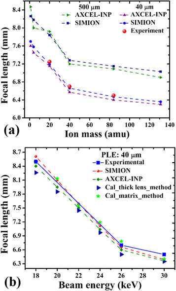
Figure 15. Variation of focal length with (a) plasma parameter, ion mass (b) beam related parameter, beam energy (EL2 voltage) [26]. Reproduced from [Maurya S K, Barman S, Pan N, and Bhattacharjee S 2019 Effect of plasma and beam parameters on focal dimensions in micrometer charged particle optics: enhanced nonlinear demagnification below the Debye length Phys. Plasmas 26 063103], with the permission of AIP Publishing.
Download figure:
Standard image High-resolution imageTable 2. Applied high voltages to the electrodes in AXCEL-INP, SIMION (simulations), and experiments. Reprinted from [26], with the permission of AIP Publishing.
| Applied high voltages to the lenses in AXCEL-INP and SIMION simulations and experiments (kV) | |||
|---|---|---|---|
| PLE aperture size (μm) | EL1 | EL2 | BL |
| 40 | −2.2 | −26 | −17.3 |
| 500 | −1.5 | −26 | −17.3 |
The negative high voltages applied to the different electrodes are tabulated in table 2.
Variation of beam size and corresponding demagnification (beam size/PLE aperture) with plasma electrode aperture size is investigated and the results are shown in figure 16. It is observed that for plasma based MEFIB, sudden decrease in beam size is observed below the Debye length (∼100 μm) and enhanced nonlinear demagnification (beam size/PLE aperture) is obtained because penetration of electric field into the plasma becomes weak for plasma electrode (PLE) apertures below the Debye length, and beam extraction decreases and therefore beam size due to reduction in space charge effects [26].

Figure 16. Variation of beam size and demagnification factor with aperture size of plasma electrode [26]. Reproduced from [Maurya S K, Barman S, Pan N, and Bhattacharjee S 2019 Effect of plasma and beam parameters on focal dimensions in micrometer charged particle optics: enhanced nonlinear demagnification below the Debye length Phys. Plasmas 26 063103], with the permission of AIP Publishing.
Download figure:
Standard image High-resolution imageNext the effect of the BL aperture size on the beam size is investigated. The BL aperture size is varied in the range 50 μm–260 μm for different PLE aperture size (∼40 μm–250 μm). At first the beam current is measured using the Faraday cup (FC) and thereafter beam spots are obtained on Cu thin films. Figure 17 shows the beam current measurement result for 100 μm PLE, and 50 μm, 100 μm and 260 μm BL aperture sizes. It is observed that with decrease in BL aperture size, beam current is found to decrease, as smaller BL trims the beam. In figure 17, sudden increase in current is observed at a particular value of EL1 voltage when the beam gets focused and maximum current is registered in the FC. Thereafter, as the EL1 voltage is increased further the beam gets defocused at the BL aperture and the current decreases due to interception of the beam by the BL. For 50 μm BL, the aperture size is very small to extract the beam and therefore results in a small current ∼5 pA. Further, SIMION beam simulation is carried out, which shows trimming of beam with increase in EL1 voltage as shown in figure 18. Variation of beam current with PLE aperture size is also studied for 260 μm BL, and has been shown in [26].

Figure 17. Variation of ion beam current with extraction voltage EL1 for different BL aperture sizes and 100 μm PLE aperture size.
Download figure:
Standard image High-resolution image
Figure 18. SIMION simulation results showing trimming of the beam with increase in EL1 voltage from (a) to (c).
Download figure:
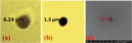
Standard image High-resolution imageFurther the beam spots are created on 50 nm Cu thin film for 100 μm PLE, and 260 μm and 100 μm BL aperture sizes. As observed in the figure 17, the beam current decreases with decrease in BL aperture size and therefore corresponding space charge effects also decrease, hence the beam size (beam diameter) is found to reduce (∼1.3 μm) for 100 μm BL, as compared to ∼6.24 μm for the 260 μm BL aperture size, as shown in figures 19(a)–(b).
Figure 19. Optical microscopy images of beam spots for 100 μm PLE and (a) 260 μm, and (b) 100 μm, BL aperture size. The beam diameters are 6.24 μm and 1.3 μm respectively. (c) Scanning electron microscopy (SEM) images of created submicron beam spots for 50 μm PLE and 140 μm BL aperture size. The beam spot diameter is 600 nm.
Download figure:
Standard image High-resolution image
Beam spots are also created by reducing PLE aperture size (source size) and minimizing the space charge effects. Source size is reduced by employing 50 μm PLE and space charge effects are minimized by trimming the beam using 140 μm BL aperture size (small beam current ∼20 pA). A submicron size beam (diameter ∼600 nm) is obtained which is analysed under scanning electron microscopy (SEM) as shown in figure 19(c).
6. Future prospects
The present MEFIB has many future applications. Firstly, the micro-glass capillary can be employed after the PLE to further reduce the beam size to sub-micron as discussed in section 3.2. By this way, the source size (PLE aperture size) can be reduced without significantly loss of beam current, where self focusing of beam through the capillary may further help to reduce the source size and therefore lead to a reduction of beam size. Secondly, the grating microstructures shown in figures 9(b)–(d) can be employed to enhance the optical properties of the materials. As reported in literature, grating type structures of periodicity comparable to the incident radiation (such as laser light) can possess different optical properties such as enhanced absorbance, negative refraction, including tailoring thermal radiation [14, 93, 94]. An array of nanoholes of sub-wavelength periodicity created on copper thin film has been used to enhance field emission which can be used in electron gun [14]. Octupole or quadrupole magnetic focusing can be utilized after the last electrode of EL2 to further compress the beam and reduce the beam spot size by arresting the expansion of the beam. Magnets focus the final beam having velocity vz by Lorentz force. By controlling PLE, BL aperture sizes and octupole or quadrupole magnet parameters, beam size can be controlled in the range of ∼μm to nm. Plasma can also modify and control the beam size as demonstrated in the realization of the nonlinear demagnification by controlling the plasma parameters. Therefore, micro to nanostructures can be fabricated as per the requirement. Additionally, as shown earlier, the total momentum transferred i.e. current normalized force can be controlled by changing the neutral gas that helps to obtain different micro to nano structures with variable aspect ratio [25] due to a variation in the momentum transferred to the substrate. It should be however borne in mind that the surface milling rates will also depend upon target sample characteristics such as electrical conductivity, crystallinity, hardness and target atomic masses.
Further applications of MEFIB beam can be demonstrated. It can be used to process the advance biomaterials without metallic contamination because of inert nature of gaseous ion beams. Ion beam processing of polyurethane and silicon rubber (polymer biomaterials) is important for applications in artificial heart valves [46]. Metallic biomaterials such as cobalt-chromium alloys (Co-Cr) and titanium or titanium alloys are used in orthopaedic prostheses. The surface properties of these alloys can be improved by processing with nitrogen ion beams, which reduces wear and tear [46]. For micro-nano fluidic applications, fabrication of complex structures is required which can be addressed using the MEFIB system [95, 96], including rapid milling that can also be achieved using the same device.
Some fundamental physics research can be carried out using this system, such as the Kapitza–Dirac effect for proton beams which can be easily obtained from the focused ion beam [97–101]. Here, two laser lights from opposite direction can be sent to the ion beam where diffraction pattern may be observed due to interaction of ion beam with the standing waves of the laser light which acts as an optical crystal. The diffraction pattern can be used to study the behaviour of ion beam such as spin dynamics of charge particles and finally their effect on the diffraction pattern. Further effect of electric and magnetic field on spin dynamics and polarization of ion beam can also be studied. In the nanometer regime, the quantum mechanical behaviour of the ion beams and their applications in the quantum regime can be an interesting research area for the future.
7. Conclusions
An overview of a microwave plasma based focused ion beam system (MEFIB) is presented including recent research results and future prospects. Starting from the advantages of a stable and contamination free microwave plasma, the device offers several advantages when compared to both liquid metal based ion sources and other plasma based focused ion beam systems currently under development around the world. With a small longitudinal energy spread ∼5 eV, the device offers the flexibility of tuning the beam current from tens of pA to tens of microamperes. The possibility of obtaining higher currents will allow rapid processing and volume milling of samples which can sometimes take days if not several hours in a conventional Ga based focused ion beam system. The possibility of varying the ionic beam species allows a huge control of momentum transferred to the substrate, which implies size-controlled nano-micro structures can be developed. Furthermore, the possibility of obtaining inert gaseous ions with no toxicity opens up new research possibilities in the area of applications to bio-materials. Ion beams successfully extracted through sub-Debye length aperture sizes of plasma electrode, leads to enhancement of the demagnification significantly, thereby opening possibilities for finer beam sizes in the nanometer regime. High aspect ratio microstructures (∼100–1000) have been created in a single beam scan which is unrealized in any conventional Ga focused ion beam system [25] at relevant energies and beam current magnitudes. A mathematical model has been developed which calculates the total momentum transferred from the beam to the target sample by defining a new parameter 'current normalized force (CNF)'. This parameter has been utilized to evaluate the efficacy of the ion beams of different gaseous atoms, in processing samples. Capillary guiding of plasma ion beams has demonstrated self-focusing of the beam which can be employed to further reduce the beam size. Particle in cell (PIC) simulations have been utilized to corroborate the experimental results of capillary guiding. Dissipated charge from the beam is calculated theoretically employing observed hysteresis area including finding the self focusing limit in capillary guiding. Further prospects and some possible applications of the MEFIB system are briefly discussed.
Acknowledgments
We gratefully acknowledge financial support from the funding agency SERB (Department of Science and Technology), Government of India, Grant No. EMR/2016/006235. One of the authors, Sudeep Bhattacharjee gratefully acknowledges support from the Sanjay and Rachna Pradhan Chair Professorship at IIT Kanpur. We most thankfully acknowledge contributions of earlier authors, Mr Sushanta Barman, Ms Nandita Pan, Dr J V Mathew, and Dr S Paul, whose collaborative papers have been referred in this article. We acknowledge Physics workshop and the Glass blowing section at IIT Kanpur for timely fabrication of components.