

Abstract
Mode multiplexing technique is a new promising option to increase the transmission capacity of on-chip optical interconnects. Multimode waveguide crossings are the key building blocks in high-density and large-scale mode division multiplexing silicon photonic integrated circuits. In this paper, we review the recent progresses on silicon-based multimode waveguide crossings. Firstly, a variety of multimode waveguide crossing schemes are demonstrated and introduced including conventional multimode interference coupler, Maxwell's fisheye lens and inverse-designed multimode interference coupler. Secondly, we also discuss some emerging applications of the inverse design algorithm in the multimode silicon devices to realize ultracompact footprint and multiple functionalities. Finally, we also give the outlook of the development prospects of on-chip multimode waveguide crossings.
Export citation and abstract BibTeX RIS

Original content from this work may be used under the terms of the Creative Commons Attribution 4.0 license. Any further distribution of this work must maintain attribution to the author(s) and the title of the work, journal citation and DOI.
1. Introduction
Over the past decades, silicon photonics offer a more promising and attractive platform to address the growing demands for optical communications [1–7], microwave photonics [8–10] and quantum information applications [11–14], due to the unique advantages of compact footprint, low cost, low power consumption and compatibility with mature complementary metal oxide semiconductor (CMOS) processes. First, benefitting from the property of high index contrast, the silicon on insulator (SOI) platform enables us to design and realize ultracompact photonic integrated devices for large-scale and high-density integrated silicon photonic systems. Second, SOI platform has a extremely wide transparency window from near-infrared to mid-infrared wavelength, which can implement the optical field with low insertion loss. In addition, the compatibility with well-established CMOS processes will combine photonic technologies and electronic technologies, enabling us to achieve desirable performance, scalability, functionality and low cost simultaneously for electronic–photonic systems [15].
Recently, on-chip optical interconnect on SOI platform, as a more promising and attractive technology, has attracted tremendous attention to alleviate the communication bottleneck and satisfy the rapidly increasing demands for high transmission capacity, low power consumption and compact footprint [16–25]. Various advanced multiplexing techniques have been utilized to improve the transmission capacity, including wavelength-division multiplexing [19–21], polarization-division multiplexing [22, 23] and mode-division multiplexing (MDM) [24, 25]. MDM technique enables us to use multiple spatial modes as independent single carriers to transfer data information, providing a new dimension to enhance the transmission capacity in a single wavelength carrier. Over the past decades, various multimode silicon photonic devices have been extensively investigated and reported for realizing MDM system, including mode (de)multiplexers [26–28], multimode bent waveguides [29, 30], polarization rotator [31], and reconfigurable multimode silicon photonic integrated circuits [32]. The high multimode waveguide crossing, as a key building block for realizing the on-chip densely integrated MDM routing and network, is still a major challenge.
In this paper, we review the recent progresses on silicon-based multimode waveguide crossings. After a brief introduction, we demonstrate and present a variety of multimode waveguide crossing schemes such as conventional multimode interference coupler, Maxwell's fisheye lens and inverse-designed multimode interference coupler in section 2. In section 3, we also discuss some emerging applications of the inverse design algorithm in the multimode silicon devices to realize ultracompact footprint and multiple functionalities. Finally, we also give the outlook of the development prospects of on-chip multimode waveguide crossings.
2. Multimode waveguide crossing
Multimode waveguide crossings are the essential components in high-density and large-scale on-chip MDM optical network. Over the past decades, many schemes have been proposed and experimentally demonstrated including conventional MMI coupler [33–35], Maxwell's fisheye lens [36–38] and inverse-designed MMI coupler [39]. The demonstrated devices with the high performance of compact footprint, low insertion loss and low crosstalk will show great potential in practical applications for high-density and large-scale MDM systems. We will introduce several types of silicon-based multimode waveguide crossing in the following.
2.1. Multimode waveguide crossing based conventional MMI couplers
Self-imaging phenomenon enables the widespread use of MMI coupler to design various silicon photonic devices including power splitters [40], wavelength multiplexers [41] and mode multiplexers [42]. Waveguide crossing could be also realized in this way by the self-imaging effect and the length of the device will be the common multiple of the beat length by different modes. For simplicity, a single-mode waveguide crossing with the high performance of low loss (∼0.02 dB) and low crosstalk (∼−40 dB) could be easily achieved by self-imaging effect [43]. The MMI length is usually set as the twice of beat length by the fundamental mode. However, it is a challenge to realize multimode waveguide crossings because the walk-off of self-imaging position by the different high order modes. This problem severely restricts the potential applications in designing on-chip high-performance multimode waveguide crossings.
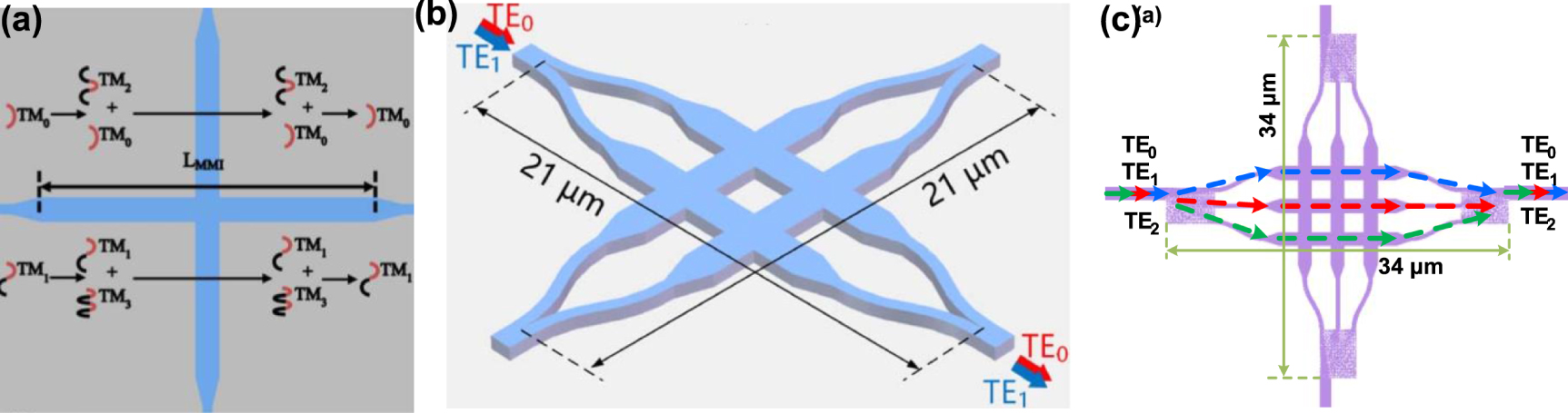
Recently, several schemes of multimode waveguide crossings based on MMI couplers were introduced and experimentally demonstrated by some special designed structures. A dual-mode waveguide crossing was proposed and demonstrated [33], as shown in figure 1(a). The proposed device is composed of two 90° crossed MMI couplers and four tapers at each input/output port. By designing the tapered waveguides optimally, the launched TM0 excite TM0 and TM1 in the MMI coupler while the launched TM1 mode can excite to the TM1 and TM3 modes in the MMI coupler. By further optimizing the width and length of the MMI coupler, the self-images for both TM0 and TM1 modes could be approximately at the center of the crossing. The fabricated device exhibited the high performance of low insertion loss (∼1.5 dB), low crosstalk below (−18 dB) and a compact footprint of 30 × 30 μm2 over a bandwidth of 80 nm.

Figure 1. On-chip multimode waveguide crossings based MMI coupler. (a) A dual-mode waveguide crossing based on MMI coupler [33]. (b) A two-mode waveguide crossing based on symmetric Y-junction [34]. (c) A three-mode waveguide crossing based on subwavelength asymmetric Y-junction [35].
Download figure:
Standard image High-resolution imageTo overcome the severe self-image position offset of different modes, Y-junction was introduced to covert the high order modes to the fundamental modes in the MMI-based multimode waveguide crossing [34]. For example, a dual-mode waveguide crossing is composed of four symmetric Y-junctions and a 2 × 2 crossing matrix, as shown in figure 1(b). The symmetric Y-junction is utilized to convert both fundamental mode and first-order mode to two in-phase or anti-phase single mode parts to avoid tackling multiplexed modes simultaneously. It works very well for two modes. The experimental result indicated the insertion loss of TE0 mode and TE1 mode were 0.46 dB and 1.82 dB at 1550 nm, respectively. The crosstalks for both modes were less than −18 dB from 1510 to 1600 nm and the compact footprint of 21 μm × 21 μm was achieved. Besides, to implement three or more modes simultaneously, the compact asymmetric subwavelength Y-junction is introduced to achieve a multimode waveguide crossing [35]. The proposed scheme could be easily expanded to implement more modes. For simplification, the three-mode waveguide crossing is designed and experimentally demonstrated as a representative. Figure 1(c) show the configuration of ultra-compact multimode waveguide crossing based on subwavelength asymmetric Y-junction. The proposed device consists of four subwavelength structure asymmetric Y-junctions and a 3 × 3 single mode waveguide crossing array based on single mode MMI couplers. The fabricated device exhibited high performance with crosstalks less than ‒20 dB and insertion losses lower than 2 dB for all the three modes over a bandwidth range of 60 nm. A compact footprint of only 34 × 34 µm2 was also achieved.
2.2. Multimode waveguide crossing based Maxwell's fisheye lens
Transformation optics offers a new route to manipulate light propagation via spatial coordinate transformations to design and realize many marvellous optical devices, including hyperlenses [44, 45], optical invisibility cloaks [46, 47] and on-chip integrated optical devices [48–50]. Recently, the Maxwell's fisheye lens (MFL) based on transformation optics (TO) designing has attracted a considerable attention to design on-chip integrated single-mode or multimode waveguide crossings [36–38, 51]. Maxwell's fisheye lens is a cylindrical or spherical lens with a gradient index (GRIN) profile, which could focus rays emanating from a point on the boundary of the lens to a conjugate point of the diagonally opposite side. As a result, the unique aberration-free imaging properties of MFL have been exploited to design low-loss and large-bandwidth single-mode or multimode waveguide crossings.
In [36], Badri et al theoretically designed and numerically evaluated a 3 × 3 and 4 × 4 multimode waveguide crossings based on polygonal Maxwell's fisheye lens. As a proof of concept, a 4 × 4 multimode waveguide crossing based on truncated octagonal MFL is designed and demonstrated, as shown in figure 2(a). To achieve the gradient index (GRIN) profile, the special-designed lenses are implemented by mapping their refractive index to the thickness of guiding Si layer. In this way, the circular MFLs in the virtual domain is transformed to a polygon in the physical domain. The simulation results indicate the device exhibited the high performance with the ultra-insertion loss of 0.5 dB and ultra-wide bandwidth of 415 nm low crosstalk covering the whole optical telecommunication bands. The intermodal crosstalk at the diagonally opposite output port is lower than −22 dB while the crosstalks at other ports are lower than −37 dB for TE0, TE1, and TE2 modes. The 4 × 4 waveguide star crossing occupied the footprint of only 27.5 × 27.5 μm2.

Figure 2. On-chip multimode waveguide crossings based MFLs. (a) Multimode waveguide crossing based on polygonal Maxwell's fisheye lens [36]. (b) Multimode waveguide crossing using transformation optics-based Maxwell's fisheye lens [37]. (c) Multimode waveguide crossing using metamaterial-based Maxwell's fisheye lens [38].
Download figure:
Standard image High-resolution imageRecently, to resolve the issue of fabrication complexity of the GRIN structures, several schemes based on Maxwell's fisheye lens have been reported and experimentally demonstrated. One approach is that the gray-scale electron-beam lithography is employed to fabricate GRIN device on a commercial silicon-on-insulator wafer with a 220 nm thick top silicon layer [37]. In principle, the universal multimode waveguide crossing using transformation optics-based Maxwell's fisheye lens can manipulate any number of waveguide modes and support any number of crossing channels. To the best of our knowledge, it is the first time that the four-channel three-mode waveguide crossing using transformation optics-based Maxwell's fisheye lens were experimentally demonstrated and evaluated, as presented in figure 2(b). The fabricated structure based on Maxwell fisheye lens can realize aberration-free imaging for each waveguide mode, which enables multiple waveguide modes to image from one side to the opposite one. Besides, a new artificial boundary conformal mapping method and semi-analytic form are developed to transform the shape and corresponding index distribution of MFL, which aims to eliminate the distinct index and wavefront mismatches between the MFL and input/output multimode waveguides. The fabricated device achieved a high performance of low crosstalk less than −20 dB, a large bandwidth of about 400 nm and a compact a footprint of 42 μm × 42 μm.
Another approach is that one use the metamaterial-based Maxwell's fisheye lens to form the equivalent gradient index profile and fabricate the multimode waveguide crossings [38]. The index-engineered silicon metamaterial is utilized to obtain the Maxwell's fisheye lens on the silicon-on-insulator platform. In this way, this scheme extremely relaxes the fabrication complexity, compared with gray-scale electron-beam lithography. Figure 2(c) shows the 3D image of the metamaterial MFL-based multimode waveguide star-crossing. The device is composed of a single star-crossing junction covered with silicon nanorod array and tapered multimode waveguides. The metamaterial with diameter-varied nano-rod array is implemented to form the Maxwell's fisheye lens, which is easy to fabricate using the CMOS compatible technology. Due to the inherent imaging property of MFL, the incident light propagates through the star-crossing section and then forms its self-image regardless of the mode order, so that all the input modes are preserved throughout the star-crossing with low losses. The fabricated 4 × 4 multimode waveguide star-crossing using metamaterial-based Maxwell's fisheye lens has a high performance of low losses less than 0.3 dB and crosstalk lower than −20 dB for both modes and occupied a compact footprint of 18 × 18 µm2.
2.3. Multimode waveguide crossing based subwavelength multimode-interference couplers
Recently, enabling one to engineer the refractive index distribution flexibly and manipulate light field at the nanoscale, free-form or digital silicon subwavelength (SW) structures have drawn tremendous attention to realize ultra-compact and highly functional on-chip devices simultaneously [52–57]. Therefore, digital SW structure could provide an additional design degree of freedom to optimize the mode effective index to realize same self-image lengths for individual modes. In our work, to overcome the walk-off of beat length for individual modes, a novel ultra-compact dual waveguide crossing based on digital silicon subwavelength multimode-interference couplers was designed and experimentally demonstrated for densely integrated on-chip mode-division multiplexing routing and communication system [39]. As shown in figure 3, by engineering the refractive indices of the lateral claddings and changing the widths of MMI couplers, the identical beat length for both modes can be achieved using the subwavelength MMI, which can decrease the scale of the device greatly. Besides, inverse-designed subwavelength structures could also provide a high degree of freedom to implement the phase profiles of the excited multimodes in MMI region at such a deep subwavelength scale, to further minimize the modal phase errors in MMI couplers and the modal mismatch between input waveguide and SW-assisted MMI couplers.

Figure 3. (a) Working principle for the dual-mode waveguide crossing. (b) and (c) Self-image beat lengths of both modes for conventional waveguide-based MMI coupler and SW structure-assisted one as a function of W1, respectively [39].
Download figure:
Standard image High-resolution imageTo improve the fabrication robustness and design efficiency greatly, we demonstrate photonic crystal-like (PhC-like) subwavelength structure and a theory-assisted direct-binary-search-based (DBS) inverse design method to optimize digital multimode waveguide crossing. On the one hand, due to lag effect, the etching depth of conventional inverse-designed nanophotonic devices may perhaps vary dramatically and randomly, which will inevitably restrict the potential pratical applications. Our proposed PhC-like SW structures, whose feature sizes are identical, can be employed to eliminate the fabrication error by lag effect [57]. On the other hand, the conventional DBS method is extremely sensitive to the initial patterns. One has to use many random initial patterns to generate many 'optimized' patterns and then select a relatively 'best' one as the final device pattern. So, it is a challenge to improve the design efficiency and device performance. To resolve this problem, we demonstrate a theory-assisted DBS inverse design method. For example, we choose a manually-set pre-designed subwavelength MMI coupler as the optimization initial pattern instead of a random one, as shown in figure 4, and expect to improve design efficiency. As expect, our simulation results indicate that theory-assisted DBS method exhibits the higher design efficiency and better device performance. In this way, we experimentally demonstrated an ultracompact dual mode waveguide crossing with high design efficiency, quite fabrication robustness and a compact footprint of only 4.8 × 4.8 μm2. The measured insertion losses and crosstalks were less than 0.6 dB and −24 dB over a bandwidth of 60 nm for both mode, respectively. Our scheme could be easily expanded to design multimode waveguide crossings that support more modes and offer a potential and attractive route to design nanophotonic devices more efficiently and robustly.

Figure 4. (a) Schematic of the dual-mode crossings based on SW structure MMI couplers. (b)−(e) The manually-set and random initial patterns. (f)−(i) The optimized patterns for the manually-set and random initials. (j) The calculated FOMs after every iteration for the manual and random initial patterns. (k)−(l) The transmission spectra for TE0 and TE1 of the four optimized devices with different initial patterns, respectively [39].
Download figure:
Standard image High-resolution imageTable 1 shows a detailed comparison of the reported various multimode waveguide crossing schemes. It can be seen that the devices exhibited high performance with ultracompact footprint and fabrication robustness, which will probably enable high-density and large scale on-chip silicon photonic integrated circuits.
Table 1. Comparison of the reported various multimode waveguide crossing schemes.
| Ref. | Structures | Insertion loss (dB) | Bandwidth (nm) | Crosstalk (dB) | Footprint (μm2) | Number of supported modes | Number of waveguide crossing |
|---|---|---|---|---|---|---|---|
| [33] | MMI coupler | 1.5 | 80 | −18 | 30 × 30 | 2 | 2 |
| [34] | Symmetric Y-junction | 1.82 | 90 | −18 | 21 × 21 | 2 | 2 |
| [35] | Asymmetric Y-junction | 2 dB | 80 | −20 | 34 × 34 | 3 | 2 |
| [36] | MFLs | 0.5 dB | 415 | −20 | 27.5 × 27.5 | 3 | 4 |
| [37] | MFLs | 2.68 | 40 | −33 | 42 × 42 | 3 | 4 |
| [38] | MFLs | 0.3 | 100 | −20 | 18 × 18 | 2 | 4 |
| [39] | Subwavelength MMI coupler | 0.6 | 60 | −24 | 4.8 × 4.8 | 2 | 2 |
3. Multimode waveguide devices based on inverse design
As discussed in section 2.3, inverse design method plays a significant role in designing the ultracompact dual-mode crossing and realizing the same beat length for both modes by optimizing refractive index distributions at the nanoscale. Here, we also discuss some emerging applications of the inverse design approach in the multimode silicon devices to realize ultracompact footprint and multiple functionalities simultaneously. Only several design degrees of freedom (five or six) are usually available in the conventional design method. Meanwhile, the designers are also required to have the essential priori known physical effect. In contrast, the advanced inverse design method can realize the characteristics of the full design space and intelligent computation, enabling us to design more compact footprint and multiple functional multimode waveguide devices.
Generally, the inverse-designed silicon nanophotonic devices may be classified into two typies: 'analog' and 'digital' silicon nanophotonic devices. For analog nanophotonic devices, the etching patterns usually have arbitrarily or random curved boundaries. Topology optimization, level-set method, adjoint method and other gradient-based methods can reduce the tremendous computational cost, which are commonly used for inverse design of analog nanophotonic devices [58]. In 2016, Frellsen et al designed and experimentally demonstrated a topology optimized ultracompact three-mode (de-)multiplexer, as shown in figure 5(a) [59]. The fabricated device occupied the ultracompact footprint of only 6.08 × 4.93 µm2. Compared with the analog nanophotonic devices, the digital ones are normally composed of tremendously discrete pixels with rectangular shapes, which enable us to dramatically release the fabrication complexity. Simple brute-force methods, such as DBS algorithm or genetic algorithm, are mostly and successfully employed to optimize the digital patterns. A digital integrated-nanophotonics polarization beamsplitter was designed using DBS algorithm and experimentally demonstrated with the ultracompact footprint of only 2.4 × 2.4 μm2, as shown in figure 5(b) [52]. To the best of our knowledge, it is the smallest polarization beamsplitter ever demonstrated. Subsequently, Sun et al designed and demonstrated a digital polarization rotator with the high performance of ultracompact footprint of 0.96 μm × 4.2 μm and large bandwidth of 157 nm [60]. Figure 5(c) shows a digital ultracompact polarization splitter–rotator on the SOI platform [61]. The length of device was only 7.92 μm and the low insertion loss of 0.2 dB was also achieved.

Figure 5. SEM image for on-chip inverse designed multimode waveguide devices. (a) Three-mode multiplexer based on topology optimization algorithm [59]. (b) An ultracompact polarization beamsplitter using DBS algorithm [52]. (c) An ultracompact polarization rotator using genetic algorithm [60]. (d) A subwavelength ultracompact polarization beamsplitter [61]. (e) Ultracompact silicon meta-structure mode exchange device [62]. (f) Ultracompact dual-mode waveguide crossing based on subwavelength MMI coupler [39]. (g) Ultracompact three-mode multiplexer based on subwavelength asymmetric Y-junction [63]. (h) Ultracompact dual-mode waveguide bend based on subwavelength asymmetric Y-junction [64]. (i) Ultracompact inverse designed dual-mode power splitter [65]. (j) Ultracompact silicon polarization rotator [66].
Download figure:
Standard image High-resolution image
The recent research progresses indicate the inverse-designed approach have already made great success in designing 'analog' or 'digital' silicon multimode nanophotonic devices. These fabricated devices exhibited ultracompact footprint, which is about two order of magnitude smaller than that of conventional waveguide ones. However, the etching feature size of analog nanophotonic device is usually random and irregular, which severely suffer from lag effect and restrict the widespread use of inverse-design methods in practical applications. Recently, vast effect has been made to improve the fabrication robustness of 'analog' nanophotonic devices. However, the complex fabrication constraints is accompanied with reduction of design freedom. Besides, the optimized device patterns based inverse-designed method is quite random and irregular and extremely sensitive to the initial pattern. More specially, for a given a functionality, design footprint, device materials and ultimate device performance are not clear and lack of theoretical prediction. To further improve the fabrication robustness and design efficiency, we use the PhC-like subwavelength structure to relax the fabrication tolerance and propose a theory-assisted DBS inverse design method based on mannually-preset initial pattern to reduce the randomness of inverse design. By taking advantage of these two features, we designed and experimentally demonstrated a variety of multimode waveguide devices with high performance ultracompact footprint and fabrication robustness. Figure 5(e)–(j) shows the fabricated multimode nanophotonic devices including mode multiplexer [63], dual-mode waveguide bend [64], dual-mode power splitter [65] and polarization rotator [66]. The proposed inverse design method and subwavelength structures provide a new option for the design of ultracompact and highly functional multimode nanophotonic devices, which will play a more and more important roles for large-scale and high-density integrated MDM routing and system. Finally, extensive effort should be made to improve the underlying optimization algorithms to enable inverse design for exploring large-scale or reconfigurable multimode nanophotonic devices, which make the widespread use of inverse-design methods in potential practical applications.
4. Conclusion
In summary, this paper has given a review for the recent progresses on silicon-based multimode waveguide crossings. A variety of multimode waveguide crossing schemes have been realized such as conventional multimode interference coupler, Maxwell's fisheye lens and inverse-designed multimode interference coupler. MMI-based multimode waveguide crossings have been developed successfully with high performances with compact footprint, low crosstalk and low insertion loss, which are very suitable for 2 × 2 multimode crossings. Maxwell's fisheye lens-based scheme is the promising and effective method for realizing the N × N multimode crossings with ultra-loss insertion and compact footprint. An ultracompact dual-mode waveguide crossing based on inverse designed subwavelength MMI coupler was also introduced and experimentally demonstrated. The footprint of the fabricated devices was about two order of magnitude smaller than that of conventional waveguide ones. Besides, the inverse design approach based on subwavelength structures offers a promising and attractive platform for designing multimode silicon waveguide devices with ultracompact footprint, high performance and multiple functionality. More attention should be paid to developing ultracompact and highly functional multimode silicon photonics, which will show great potential in practical applications for large-scale and high-density integrated MDM routing and system.
Acknowledgments
National Natural Science Foundation of China (61775069), Technology Innovation Program of Hubei Province of China (2018AAA037, 51911530159) The Graduates Innovation Fund of Huazhong University of Science and Technology (2019ygscxcy041).