

Abstract
We present in this paper the vertical integration of an electro-absorption modulator (EAM) onto a vertical-cavity surface-emitting laser (VCSEL). We discuss the design, fabrication, and measured characteristics of the combined VCSEL and EAM. We previously demonstrated a standalone EAM with an optical bandwidth around 30 GHz. In this paper we present for the first time an optical bandwidth of 30 GHz for an EAM integrated onto a VCSEL. This device exhibits single-mode operation and a very low chirp, below 0.1 nm, even with a modulation depth of 70% which makes this device very competitive for high-speed communications in data centers.
Export citation and abstract BibTeX RIS

Original content from this work may be used under the terms of the Creative Commons Attribution 3.0 licence. Any further distribution of this work must maintain attribution to the author(s) and the title of the work, journal citation and DOI.
1. Introduction
Nowadays, vertical-cavity surface-emitting lasers (VCSELs) receive a lot of attention for their versatility in different emerging applications requiring massively expanding data transmission rates. In particular, in very recent years, new applications including internet of things, virtual reality, cloud computing and storage, have driven the demand for a significant expansion in capacity of short-reach links in data centers [1], favouring solutions with low power consumption. In that context, VCSELs bring many advantages to optical transceivers, such as a high density of integration and an easy coupling to optical fibers, making them ideal as light sources for very high-frequency and high-capacity data links.
Direct modulation on short wavelength VCSELs (850, 940 or 980 nm) has been greatly improved through many device design strategies, but the performances are restricted by different intrinsic physical limitations including carrier-photon dynamics, parasitic electrical losses, and self-heating. Albeit, VCSELs with impressive performances have been demonstrated in the past years reaching modulation frequencies in excess of 25 GHz [2–4]. In particular, VCSELs with very small oxide confinement apertures (down to few micrometers in diameter) have been found to increase the modulation bandwidth to above 30 GHz [5, 6], but at the expense of a very stringent fabrication and a potentially-compromised reliability [7]. Nevertheless, using directly-modulated devices with complex but more efficient modulation formats such PAM-4 or Discrete MultiTone have enabled optical data systems to reach transmission rates in the range of 100 Gbps on single channel links [8–10].
In order to reach even higher communication speeds, the configuration based on externally modulated laser (EML) is more adapted and advantageous as established in long and medium-range links with systems exploiting distributed feedback lasers that are in-wafer-plane integrated with an electro-absorptive modulator (EAM). The implementation of such EML with VCSEL sources would allow their respective inherent advantages to be combined and should facilitate very high speed data transfers with low power consumption to be obtained.
Indeed, in the case of the vertically integrated EAM-VCSEL, the frequency modulation bandwidth is limited by the EAM frequency response, and no longer by the optoelectronic dynamics and the thermal effects of the VCSEL. As early demonstrated in [11], the asymmetric Fabry–Perot modulator (AFPM), used in our proposed EAM-VCSEL structure, is primarily limited in frequency bandwidth by the RC electrical characteristics, and not by the carriers escape rate. This limit is inherent to the quantum confined Stark effect which only relies on the field switching time delay. The highest modulation frequency demonstrated so far for AFPM is 37 GHz [11].
The chirp is dependent on the spectral spacing between the AFPM resonance and the modulated signal wavelength[11]. This corresponds for EAM-VCSEL device to the detuning between the VCSEL and the EAM cavity resonances, which can be optimized to tailor the device chirp within a given system.
The asymmetric Fabry–Perot EAMs are also very advantageous regarding their energy consumption. As shown in [12], this type of vertical modulator can operate with a consumption as low as 10 fJ bit−1, to be compared with 100 fJ bit−1 for oxide-confined directly-modulated VCSELs [2].
Despite these potential benefits, such a vertical EML configuration has been scarcely studied and developed to-date. Practically, the co-integration of a VCSEL with a modulator has been achieved using either a lateral [13] or a vertical integration scheme.
Nevertheless, the lateral coupling presents a low extinction ratio below 4 dB and moreover, the suitable coupling regime for enabling high modulation rate may be difficult to achieve while preserving well-controlled transverse optical properties of the VCSEL beam. Also, the optical feedback can be detrimental regarding the wavelength chirp.
In the vertical configuration, the emitter amplitude modulation is introduced by an electro-refractive (ER) (phase) modulation embedded in an interferometer or by electro-absorption modulation. The former exploits quantum wells (QW) positioned in the top Distributed Bragg Reflector (DBR) mirror of the VCSEL, converting the voltage-driven modulation of the QW refractive index into an amplitude modulation through the change of the mirror effective reflectivity [14–16]. If modulation bandwidths greater than 10 GHz have been obtained [15, 16], the prime limitation of this approach is its inherent large chirp resulting from the significant variation of the device effective cavity length [17, 18].
To avoid the latter drawback, a more promising approach to implement the modulation relies on using the electro-absorption phenomenon as done in [19]. In this case, the EML structure consists of three DBR mirrors defining two weakly-coupled cavities, each of which containing QWs, where the bottom cavity is current-driven to operate as the emitter and the top cavity is voltage-driven to induce the modulation. A modulation at 20 GHz was demonstrated by proper detuning of the EAM and VCSEL cavity resonances [20].
Higher bandwidths could be achieved if the parasitic capacitances and resistances are further reduced [21]. Temperature control is also a challenge to preserve low-power consumption and a reduced chirp size. The development of these two last points have been the main items of our work and will be presented in this paper.
We present in this paper a device based on the proposed concept of Van Eisden et al [20], the vertical integration of an electro-absorption modulator onto a VCSEL. We describe in the first section the structure and the fabrication of this three-electrode device. Then we demonstrate the efficiency of this device with static characterization. Finally, the high-frequency modulation results will be discussed.
2. Structure description and fabrication
The EAM VCSEL structure was grown, with an N–P–N doping profile, monolithically in a single epitaxial run on an N-doped GaAs substrate using a RIBER 412 molecular beam epitaxy (MBE) system.
Above the substrate, the structure combines a conventional 850 nm VCSEL structure stacked with an AFPM structure.
The VCSEL part is formed by a 35.5 period Al0.9GaAs/Al0.15GaAs N-type bottom DBR, a half-wave thick optical cavity including three GaAs/Al0.3GaAs quantum well/barrier layers (QW), and a 12.5 periods P-type DBR embedding an Al0.98GaAs 30 nm thick layer for oxide confinement in the first period above the cavity. Above that, a P-type 3λ/4 thick layer is grown to serve commonly as the top-electrode of the VCSEL and the bottom-electrode of the EAM. Above, the AFPM structure is grown composed of a 10.5-period P-doped DBR (with the same composition as used in the VCSEL's DBRs), a 2λ thick undoped cavity embedding 25 GaAs/Al0.3GaAs QWs, and finally capped by an N-doped 6.5-period DBRs and a 50 nm GaAs cap as an N-contact layer.
The common intermediate DBR was deliberately chosen to be thick enough (23 periods overall) to minimize the coupling between the VCSEL cavity and the EAM cavity to reduce the impact of the coupled vertical cavities on optical feedback that may impact the VCSEL performance while enabling high-depth modulation. Also, a not too high top mirror reflectivity as seen by photons in the VCSEL cavity have to be kept to not decrease the output power.
The second crucial point is the wavelength detuning between the VCSEL cavity (respectively AFPM cavity) resonance and the VCSEL gain (resp. AFPM QWs absorption tail) to ensure operation over a large temperature range. Typically a redshift room temperature cavity detuning of about 15 nm with respect to the QW photoluminescence peak leads to a perfect gain-to-cavity alignment around 40 °C–50 °C, when the integrated AFPM undergoes about the same heating as the VCSEL.
Furthermore the VCSEL and AFPM cavity resonances are slightly offset to avoid optical feedback between both cavities, as shown in [19].
Following the epitaxial growth of the EAM VCSEL structure, the respective wavelength detunings were measured by top reflectivity and photoluminescence (PL) of the global epitaxial structure and after successively etching this structure down to the top of the EAM and laser cavity respectively. The measured cavity to peak PL offsets are +23 and +22 nm respectively for the VCSEL and the EAM, while the VCSEL cavity resonance is redshifted by 5 nm with respect to the EAM cavity resonance wavelength.
Subsequently, the devices were fabricated with triple contact electrodes to independently bias the VCSEL and the EAM. Also, to facilitate high frequency (HF) operation, the whole 6 μm thick EAM VCSEL was planarized with BCB, and a low-loss microstrip injection scheme was implemented to drive the modulator. The details of the HF pad design and processing will be published elsewhere [22].
A schematic of the final device is shown in figure 1. The vertical and horizontal scaling factors are deliberately chosen to differ to give a clear view of the device.

Figure 1. Global view of the fabricated EAM VCSEL device with microstrip line access for RF signal injection.
Download figure:
Standard image High-resolution image3. EAM VCSEL static characterization
Figure 2 presents the light-current (LI) response of the VCSEL at room temperature while applying different static voltages to the modulator.
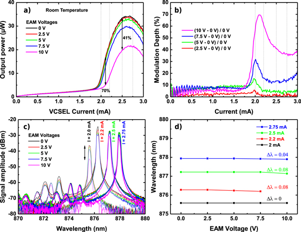
Figure 2. (a) L-I curve of the EAM VCSEL structure at room temperature. The output power is plotted for different EAM voltages. (b) is the modulation depth function of the applied EAM voltage. (c) Emission spectra under different EAM bias voltages. (d) Extraction of the wavelength shift when the VCSEL is modulated.
Download figure:
Standard image High-resolution imageIn figure 2(a) the modulation effect can clearly be seen on the LI curve with insignificant change of the lasing threshold current demonstrating uncoupled operation of the two cavities. As shown on figure 2(b), the modulation depth reaches 70% for a voltage change of 10 V across the EAM and a VCSEL operating just above threshold. We can note that a modulation depth surpassing 40% can be reached all over the LI curve, showing that the modulation can be applied for any values of the output power from the VCSEL.
The optical spectra have also been measured with an optical spectrum analyser as shown in figure 2(c), for different VCSEL currents and different voltages on the EAM. A redshift of the laser emission is observed when the driving current rises according to the inherent temperature increase in the structure. In contrast, at a given laser injected current, the wavelength remains essentially unaffected by the EAM applied voltage (see figure 2(d)). The maximum wavelength chirp reaching 80 pm is observed to occur when the modulation depth is maximal.
4. EAM VCSEL HF modulation
Standalone EAM structures were first characterized by measuring the top reflectivity at a fixed wavelength using a single-mode fiber optical injection/collection and driving the modulator with the HF voltage signal injected using a cascade Infinity 67 GHz GSG-150 probe. A tunable laser source was used as a monochromatic illumination source on the top of the EAM, and a fiber coupler enabled the collection of the reflected signal. A FieldFox Keysight was used to extract the EAM frequency response through a high-speed photodiode. Details of this measurement setup is given in [23]. The EAM standalone vertical modulators exhibit modulation bandwidths in the range of 28–32 GHz, for modulator diameters ranging from 26 to 18 μm, respectively.
Also for HF characterizations of both the EAM and the EAM VCSEL structures, the injection losses due the different RF elements in the setup were carefully characterized and compensated for in order to retrieve the real input and output powers to/from the studied modulator devices [23]. In particular, the frequency response of the New Focus 1434 InGaAs photodetector used for the measurements was measured by a heterodyne technique for an 850 nm wavelength giving a f−3dB of 27 GHz, and hence the measured response was included to extract the effective modulation amplitude of the EAM up to 40 GHz.
The EAM VCSELs were next characterized by applying the HF voltage generated by an Agilent PNA-X vectorial network analyzer with a range extending up to 67 GHz. The presented results were measured on a 71 μm diameter VCSEL, with an oxide aperture diameter smaller than 5 μm, topped by a 24 μm EAM. The normalized frequency response of the EAM VCSEL devices is shown in figure 3 with an applied current of 2.9 mA on the VCSEL section and a DC bias of 8.5 V on the EAM. The injected modulated voltage amplitude is estimated to be <1 V in the full range of frequencies due to the limited power delivered by the VNA and the high impedance of the EAM itself. In agreement with the previous results on a standalone EAM, a −3dB modulation bandwith as high as 29 GHz has been measured. This result shows clearly the advantage of decoupling the modulator section from the VCSEL emitter, and indeed the potential gain compared to directly-modulated VCSELs. For comparison, these results show a significant improvement compared to the results from [19] on a similar EAM VCSEL structure. This last structure contains a thicker intermediate DBR separating the two cavities, and multiple double QWs which serves as the modulated absorbing region. Regarding the HF injection configuration, our design seems to be more optimized in terms of reduced HF injection losses, including the use of a 2-λ thick cavity for reducing the device capacitance compared to a 1.5-λ thick cavity.

Figure 3. Modulation frequency response at room temperature of the EAM VCSEL. The VCSEL is powered at 2.9 mA and the EAM at 8.5 V.
Download figure:
Standard image High-resolution imageThe frequency response of the EAM VCSEL device was also studied for different EAM DC bias, in order to check the influence of the working point on the absorption curve on the dynamics (in figure 4). As already reported in [20], the DC bias applied on the modulator noticeably modifies the shape of the frequency response. In particular, a strong resonance peak arises around 3 GHz, and is strongly dependent on the bias voltage. In the inset of figure 4 we plotted this relaxation frequency against the bias voltage on the EAM. When increasing the bias, this peak goes to a minimum frequency at 2.5 GHz while decreasing in intensity, until it vanishes for a bias of 8.5 V, for which the frequency response is flat up to 20 GHz. For higher values of the bias, the resonance peak arises again, and its frequency increases again towards the same frequency observed at low biases.

Figure 4. Modulation frequency response at room temperature of the EAM VCSEL under different DC bias on the EAM section. Inset: frequency of the resonance peak around 3 GHz as the function of the EAM bias.
Download figure:
Standard image High-resolution image
The frequency response can be understood as the modulator stand-alone response combined to an undesired though often-present loss-modulated laser response originating from the coupling between the modulator and laser cavities. Indeed, as explained in [20], the EAM modulation also induces an additional mirror reflectivity change which, in-turn, impacts the photon density in the laser cavity and gives rise to the observed relaxation resonance frequency. Nevertheless, this resonance can be avoided by tuning the EAM bias (uncoupling the cavities), enabling a significant increase in the modulation bandwidth but at the expense of a reduced power in modulated signal.
We also observe on standalone EAM devices that, even though the modulation contrast changes with the temperature, the 3 dB frequency remains constant in the investigated range between 15 °C and 55 °C.
5. Conclusions
We have demonstrated the fabrication and the characterization of a new monolithic configuration of an EAM VCSEL, in which the gain and the modulation cavity resonances are optically decoupled. The effective modulation through an AFPM based on electro-absorption allows us to achieve a large modulation contrast while ensuring a very small wavelength chirp compared to devices that operate via the ER effect. The fabrication of the EAM VCSEL device has been realized with a low loss RF injection microstrip line access and properly planarized thick BCB layer. The high-frequency modulation on this EAM VCSEL device has been successfully demonstrated up to 29 GHz with a flat response through the adjustment of the applied bias on the modulator. This modulation bandwidth is to our knowledge the best achieved on this type of electro-absorption modulated VCSEL.
Acknowledgments
The authors gratefuly acknowledge the technological support of RENATECH (French Network of Technology Platforms) within the LAAS-CNRS cleanroom infrastructure and the financial support of the Methusalem foundation, Belgium.