

Abstract
Janus two-dimensional (2D) materials, referring to the layers with different surfaces, have attracted intensive research interest due to the unique properties induced by symmetry breaking, and promising applications in energy conversion. Based on the successful experimental synthesis of Janus transition metal dichalcogenides (TMDC), here we present a review on their potential application in photocatalytic overall water splitting, from the perspectives of the latest theoretical and experimental progress. Four aspects which are related to photocatalytic reaction, including the adsorption of water molecules, utilization of sunlight, charge separation and transport, and surface chemical reactions have been discussed, and it is concluded that the Janus structures have better performances than symmetric TMDCs. At the end of this review, we raise further challenges and possible future research directions for Janus 2D materials as water-splitting photocatalysts.
Export citation and abstract BibTeX RIS

Original content from this work may be used under the terms of the Creative Commons Attribution 4.0 license. Any further distribution of this work must maintain attribution to the author(s) and the title of the work, journal citation and DOI.
1. Introduction
Due to the continuous growth of energy crises and environmental pollution, photocatalysis, as a promising technology to simultaneously solve these two problems by utilizing solar energy, has attracted significant interest in recent years. Using the photogenerated electrons and holes of photocatalysts, H2O can be split into the value-added chemical fuels, hydrogen and oxygen, which is a 'green' route to converting solar energy into chemical energy without environmental pollution [1–3]. The recently emerged two-dimensional (2D) layered materials have exhibited great potential for photocatalytic applications due to the large surface–volume ratio, numerous catalytic reactive sites, and the ability of good optical adsorption. The tunable electronic structures which strongly depend on the layer thickness and external stimuli facilitate the optical adsorption and the optimal band alignments relative to the redox potential of water. More importantly, the ultrathin thickness and short carrier migration distance could prevent the recombination of photogenerated carriers to some degree. Therefore, 2D materials usually possess better photocatalytic performances than their bulk counterparts. However, until now, the achieved photocatalytic efficiency of 2D materials is not as high as expected due to some practical reasons. Typically, an ideal photocatalyst has to be stable under atmospheric environments and semiconducting with medium band gaps for optical spectrum adsorption. The first requirement limits the potential candidates to mainly graphene, hexagonal boron nitrides, and transition metal dichalcogenides (TMDCs). The second criteria further exclude graphene because of its semimetal feature, and boron nitrides due to the large band gaps, as insulators. Owing to the suitable bandgap and excellent stability, an enormous number of TMDCs have been regarded as promising candidates for the photocatalytic water splitting application [4, 5]. However, the structural symmetry along the out-of-plane direction cannot separate the photoinduced charges well, which limits the photocatalytic conversion efficiency.
The asymmetric Janus TMDCs, which have recently been synthesized, inherited the advantages of 2 H-phase TMDCs, but provide an additional degree of freedom to tune/improve the photocatalytic performance for water splitting. The typical structure of these Janus TMDCs is shown in figure 1(a), where the transition metal layer is sandwiched by two different chalcogen layers. The structural symmetry along the out-of-plane direction is therefore broken, leading to the different electronic, optical, and photocatalytic performances which can distinguish Janus materials from 2 H-phase TMDCs. The intrinsic dipole, caused by structural asymmetry in 2D Janus materials, could improve the spatial separation between photo-excited electrons and holes, preventing the carrier recombination. Based on the reaction mechanism proposed by Yang et al, water splitting using incident near-infrared light could be realized in 2D polar photocatalysts, where the valence band and conduction band locate at the two opposite surfaces with a large electrostatic potential difference caused by the intrinsic dipole [6]. This will substantially enhance the light utilization efficiency. Motivated by these beneficial properties, a large number of 2D Janus single layers (SLs) and bilayers (BLs) have been designed for the application of photocatalytic water splitting, such as III2XY (III = Ga and In; X, Y = S, Se, and Te, and X ≠ Y) SLs [7, 8], MXY (M = Mo, W) SL and BL [9–13], ScXY SLs [14], PtSSe SL and BL [15], and MXZ (M = Zr, and Hf; X = S and Se; Z = O and S; X ≠ Z) SLs [16]. Based on the reaction mechanism, photocatalytic water splitting can be divided into four steps (see figure 1(b)): (1) adsorption of water molecules, (2) utilization of sunlight, (3) charge separation and transport, and (4) surface hydrogen evolution reaction (HER) and oxygen evolution reaction (OER). Each of them can significantly affect the efficiency of photocatalysts. Therefore, in the following we will introduce the photocatalytic properties of Janus 2D materials from the four perspectives, and make the corresponding comparison with the symmetric 2 H-phase MX2 and MY2 materials. At the end of the review, the further challenges and possible research directions have been discussed for Janus 2D materials.

Figure 1. (a) The atomic structure of the Janus MXY (X, Y = S, Se, and Te; X ≠ Y) monolayer. (b) A schematic illustration of photocatalytic water splitting based on the Janus MXY monolayer. The yellow, pale green, red and, grey balls represent the Y, X, oxygen, and hydrogen atoms, respectively. Similar to the Z-scheme heterojuction [17], due to the electrostatic potential difference at the top and bottom surfaces of the Janus MXY (X, Y = S, Se, and Te; X ≠ Y) monolayer, the redox potential of H+/H2 and H2O/O2 at the two surfaces are not uniform.
Download figure:
Standard image High-resolution image2. Experimental synthesis of Janus TMDCs
Although the Janus TMDC structure with two different surfaces was theoretically proposed in 2013 [18], they were synthesized until very recently due to the experimental challenges of uniformly replacing one surface with a different chalcogen element. Therefore, although there were numerous studies regarding TMDCs with chalcogen impurities like MoS2(1–x)Se2x, they were randomly substitutionally doped. Due to the progress in experimental equipment and techniques, the Janus structure (a sandwich structure with the central metallic layer and two marginal layers of different chalcogen atoms) can be fabricated using the modified Chemical Vapor Deposition (CVD) method. As shown in figure 2(a), Zhang and co-workers synthesized Janus SeMoS using the following steps: the top-layer S atoms of the synthesized MoS2 SL is firstly replaced by H atoms with a remote hydrogen plasma (Janus HMoS SL formed); then, the H atoms of HMoS SL are replaced by Se atoms with a thermal selenization (Janus SeMoS SL formed) [19]. Soon after, as displayed in figure 2(b), Lou and co-workers also independently fabricated the SMoSe SL using the sulfurization method. More specifically, the top-layer Se atoms of MoSe2 SL were directly replaced by S atoms through a sulfurization at the appropriate temperature (750 °C ~850 °C) [20]. With the exception of these two works, there was little experimental progress on the fabrication of Janus TMDC SLs afterwards. Recently, Pan and co-workers synthesized WS2(1−x)Se2x SL by heating WS2 and WSe2 mixed powders at 1000 °C; the WS2-WS2(1−x)Se2x lateral heterostructure was fabricated by changing the chemical vapor source interactively using a direction-controlled argon flow [21]. The Se mole fraction (x) could be tuned from 0.06 to 1 by modulating the composition of the mixed powder. Unfortunately, there is no concrete evidence to prove the WS2(1−x)Se2x SL has a Janus structure.

Figure 2. (a), (b) A schematic illustration of the reaction setup for the fabrication of the Janus MoSSe monolayer with the two different CVD methods. (a) Reprinted by permission from Macmillan Publishers Ltd: [Nature Nanotechnology] [19], Copyright (2017). (b) Reprinted with permission from [20]. Copyright (2017) American Chemical Society.
Download figure:
Standard image High-resolution imageBased on the experimental progress, novel electronic properties of Janus SLs have been found, such as a huge piezoelectric effect, robust Rashba spin splitting, a second-harmonic generation (SHG) response [19], and high basal plane HER catalytic activity [20]. They can result in the interesting applications in gas sensors, piezoelectric devices, thermal electric devices, solar cells, ion batteries, and so on. In the review, we mainly focus on its application to photocatalytic water splitting, and discuss the advantages/disadvantages compared with out-of-plane symmetric TMDCs (with the same chalcogen atoms at two surfaces).
3. Adsorption of water molecule
As a key issue in the electrochemistry and geochemistry fields, water interaction with solid surfaces has received a great deal of attention [22–24]. The photocatalytic water splitting could be defined by the following two half reactions, respectively [25, 26],

Hence, adsorption of H2O on the surface of a photocatalyst is the first step of the catalytic reaction; the adsorption strength is regarded as an important parameter characterizing its activity in the photocatalytic water-splitting application. For the MoS2 layer, the water molecule is generally weakly adsorbed on the surfaces; the water splitting reaction can only occur when the defects and edges with dangling bonds are present which can chemically bond with the water molecules. More interestingly, as illustrated in figure 3(a), it has been found that, with an applied perpendicular electric field, both the gas selectivity and sensitivity could be significantly modulated because of the tunable electron transfer between gas molecules and the substrate material [27]. Therefore, it can be expected that the intrinsic dipole in Janus 2D materials induced by the out-of-plane asymmetric structure could strengthen the adsorption of the H2O molecule on the surface, which can provide a better platform for catalytic reaction. From the theoretical simulations, it was indeed found that, due to the intrinsic dipole, the binding energy of H2O on the S side of MoSSe is about 0.04 eV larger than that on the MoS2 monolayer [9]. However, the H2O molecule is still bonded to the surface of MoSSe SL mainly with the weak van der Waals (vdW) force, which may be an obstacle in its photocatalytic water-splitting application. Fortunately, as displayed in figures 3(b) and (d) transition metal adatoms (Sc−Ni) could regulate the dipole moments of Janus MoSSe SL efficiently [28]. And the adsorption of suitable transition metal atoms could also bring about the transition of the interaction between H2O and MoSSe from electrostatic vdW forces to strong chemical bonding, significantly strengthening the adsorption of the H2O molecule (see figure 3(c)), which paves the foundation for the following catalytic reactions [29]. In addition, it has been reported that BL Janus MoSSe is a better gas sensor material [30], so that they can have a stronger adsorption behaviour of the water molecule due to the superposition of the polarization.

Figure 3. (a) Variation of charge transfer as a function of the electric field strength for NO and NO2 molecules adsorbed on a MoS2 monolayer. (b) Dipole moments and bader charges for the adsorption of TM atoms on the S surface and Se surface with different adsorption sites. (c) The adsorption structures of H2O on both (S and Se) sides of the pure and TM-modified MoSSe. (a) [22] (2013) (© 2020 BioMed Central Ltd). With permission of Springer. (b) Reprinted with permission from [23]. Copyright (2019) American Chemical Society. (c) Reprinted with permission from [24]. Copyright (2019) American Chemical Society.
Download figure:
Standard image High-resolution image4. Utilization of sunlight
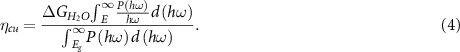
The utilization of sunlight is directly related to the photocatalytic efficiency, which could be evaluated by the solar-to-hydrogen (STH) efficiency (ηSTH), defined as the product of the efficiency of light absorption (ηabs) and carrier utilization (ηcu) [31]:

Because of the structural and chemical similarity, the band gaps of Janus 2D TMDCs are normally among the values of their parent materials [9, 12, 32]. The efficiency of light absorption is defined as [31]:

where  are the AM1.5 G solar energy flux at the photon energy
  , and Eg is the direct band gap of the photocatalyst. Hence, the efficiency of light absorption of the Janus 2D MXY is also among the values of their parent materials (MX2 and MY2).
However, the case for the carrier utilization is different. The efficiency of the carrier utilization ( ) is defined as [31]:
Here,  is the free energy of water splitting (1.23 eV) and the rest of the numerator represents the effective photocurrent density. Here, E represents the photon energy that can actually be utilized in the process of water splitting [31].

where and
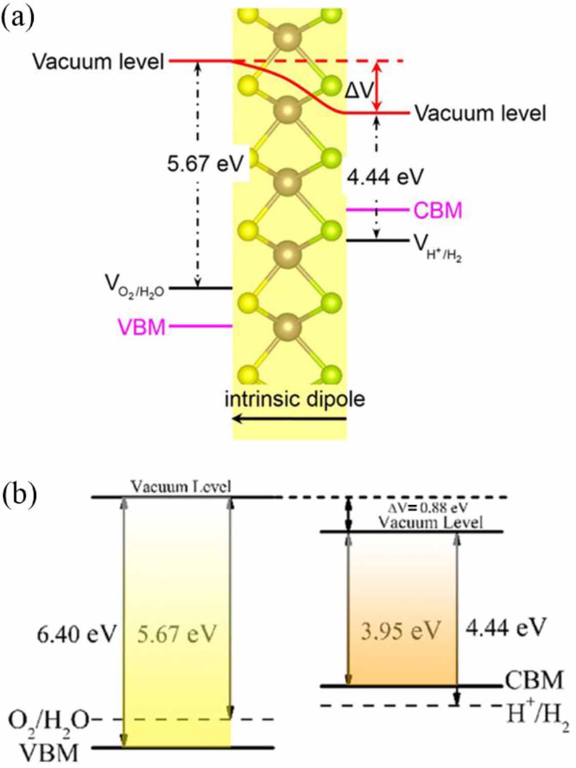
and  represent the overpotentials for the HER and OER, respectively. According to the reaction mechanism proposed by Li et al [6], as shown in figure 4, the intrinsic dipoles in the Janus 2D materials help to shift the redox potentials [9, 32], which will raise
  and
and  . After considering the contribution of the intrinsic electric field for the electron–hole separation into the total energy, the corrected STH efficiency of photocatalytic water splitting for 2D material with a vertical intrinsic electric field could be calculated as:

where  is the vacuum level difference on the two respective surfaces.

Figure 4. (a) A schematic plot of energy levels for the MoSSe monolayer. Here, ΔV denotes the potential difference between the two sides of the MoSSe that is induced by its intrinsic dipole. The difference in energies between the CBM and VBM are equal to the sum of the band gap and the potential difference (ΔV) between the two sides. (b) Band alignments of the CrSSe monolayer based on the G0W0 level. (a) Reprinted with permission from [9]. Copyright (2018) American Chemical Society. (b) Reprinted with permission from [32]. Copyright (2019) American Chemical Society.
Download figure:
Standard image High-resolution imageAs listed in table 1, we select the cases of the Janus MoSSe SL, MoS2, and MoSe2 to show the STH difference. The efficiencies of light absorption of these three materials are in the same order as the band gaps. But due to the rise in the redox overpotential caused by the vertical intrinsic dipole, the Janus MoSSe SL has a much larger efficiency of carrier utilization. When the efficiency of light absorption and carrier utilization are taken into account together, one can find that the Janus MoSSe SL has the highest STH efficiency. When the correction in equation (6) is considered, the corrected STH efficiency of the Janus MoSSe SL is still obviously larger than the STH efficiency of its two parent materials. Moreover, since the electronic properties of nanomaterials can be well adjusted by external stimuli, it has been found that tensile strain and transition metal atom adsorption could strengthen optical absorption [9, 29]. More interestingly, in 2D Janus MoSSe BL, the light absorption can be improved effectively by changing the stacking configurations [10, 11, 15].
Table 1. Overpotential for the HER χ(H2), overpotential for the OER χ(O2), direct band gaps at HSE06 level, and the difference in electrostatic potential (ΔV) between top and bottom surfaces, energy conversion efficiency of light absorption (ηabs), carrier utilization (ηcu), STH (ηSTH) and corrected STH (η'STH) of MoS2, MoSe2, and MoSSe monolayers.
| χ(H2) | χ(O2) | Egd(HSE) | ΔV | ηabs (%) | ηcu(%) | ηSTH(%) | η'STH(%) | ||
|---|---|---|---|---|---|---|---|---|---|
| MoS2 | 0.24 [33] | 0.63 [33] | 2.10 [33] | 0 | 31.93 | 47.45 | 15.15 | – | |
| MoSe2 | 0.59 [34] | 0.07 [34] | 1.89 [34] | 0 | 41.28 | 21.29 | 8.79 | – | |
| MoSSe | 0.74 [9] | 0.83 [9] | 2.02 [9] | 0.78 [9] | 35.28 | 48.59 | 17.14 | 15.46 | |
5. Charge separation and transport
Janus TMDCs distinguish themselves by symmetric counterparts with the distinct surface and associated out-of-plane polarization, which not only affect the band structure and optical adsorption as indicated above, but also lead to the charge separations. The latter results are expected to significantly boost the photocatalytic efficiency, as demonstrated by the recent works about polarization-enhanced overall water splitting in a ferroelectric III2X3 monolayer [31]. Due to the intrinsic dipole, the valence band maximum (VBM) and conduction band minimum (CBM) tend to distribute on the different sides of Janus 2D materials. In sharp contrast, both the VBM and CBM of traditional TMDCs are localized in the same area, which remarkably increases the possibility of photoinduced carrier recombination [8, 9, 32]. Taking CrS2, CrSe2, and Janus CrSSe as examples, shown in figure 5(a), both the CBM and VBM of CrS2 and CrSe2 monolayers distribute around the middle layer with a large overlap between each other, while the CBM and VBM of the Janus CrSSe monolayer mainly reside around the lower and upper layer, respectively. Generally, in polar semiconductors, the electrons are excited by photons from the negatively charged atoms to the positively charged ones [35]. Hence, for Janus CrSSe, the Cr states near the VBM are not excited under illumination, while the electrons of S states near the VBM are excited by photons and jump to the CBM, generating photo-excited holes and electrons. With the built-in electric field along the vertical direction pointing from Se to S, the photo-excited electrons will migrate to the CBM of the Se atoms. As a result, the spatial separation of photogenerated carriers is realized. The separation not only lowers the recombination of carriers, but also spatially separates the reaction products (H2 and O2 molecules).

Figure 5. (a) Side views of the partial charge density distribution for the VBM and CBM of the CrS2, CrSe2, and CrSSe monolayers. (b) A schematic diagram of the charge transfer mechanism and band edge position over Te–S stacking, Te–Se stacking, and Te–Se defect stacking under visible light irradiation. (a) Reprinted with permission from [32]. Copyright (2019) American Chemical Society. (b) Reproduced from [36] with permission of The Royal Society of Chemistry.
Download figure:
Standard image High-resolution imageBesides the charge separation in the single materials induced by the intrinsic polarization, the heterostructure photocatalysts with type-II band alignment are an alternative effective approach for achieving the spatial separation of photo-excited carriers. In this sense, the heterojunctions based on Janus 2D material have been designed for the effective photocatalytic water splitting, such as MoSSe/XN (X = Al, and Ga) [37], MoSSe/WSSe [13], and MoSSe/WSeTe [36]. In particular, the Janus MoSSe/WSeTe heterojunction in the Se-W-Te-S-Mo-Se stacking type is theoretically predicted to be a potential direct Z-scheme photocatalyst for H2 production. As displayed in figure 5(b), both changing the stacking configurations and introducing surface chalcogen vacancies could switch the charge transfer path from type II to the Z-scheme by modulating the competition between carrier separation and interlayer carrier recombination [36].
The charge transport is also very important for the photogenerated carriers to quickly arrive at the active site at the surface. Normally, the carrier mobility is used to evaluate the charge transport, which could be calculated by the deformation potential theory [38], as follows [39, 40]:
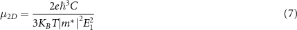
where T, e, KB, and ħ are the room temperature (300 K), electron charge, Boltzmann constant, and reduced Planck constant. Here, E1 is the deformation potential constant, which can be calculated as:

where Eedge is the energy of the band edges, and  is the uniaxial strain. At the same time, C is the in-plane stretching modulus, which can be obtained as:

where Etot is the total energy, and S0 is the area. In addition, according to the band structures, the effective masses of holes ( ) and electrons (
 ) could be evaluated by fitting parabolic functions to the VBM and CBM:

where k is the wave vector, while Ek is the energy related to the wave vector k. Similar to the gap, due to the structural and chemical similarity, the values of the carrier mobilities of 2D Janus materials are usually intermediate between those of their parent materials. As listed in table 2, we take the Janus MoSSe as an example to carry out a discussion in detail. For both the electron and hole, the mobility is in the order of  . Usually, the huge disparity between the mobility of the electron and hole will effectively prevent the combination of photo-excited carriers, increasing the photocatalytic efficiency. In MoSSe SL, the μh is more than 4 times the μe, but only 3.6 and 2.1 times in MoS2 and MoSe2 SL, respectively. Therefore, the spatial separation of photogenerated carriers could be further enhanced by the huge carrier mobility disparity in the 2D Janus materials.
6. Surface chemical catalytic reaction
When the photo-excited carriers successfully arrive at the active surface sites of photocatalysts, they need enough redox potential and driving force to take part in the water oxidation–reduction reactions (equation (1)). The sufficient redox potential for fully photocatalytic water splitting requires that the CBM should be higher than the reduction level of hydrogen (−4.44 eV at pH = 0), and the potential of the VBM should be lower than the oxidation level of oxygen (−5.67 eV at pH = 0). As mentioned above, the intrinsic dipoles in the Janus 2D materials help to shift the redox potential. Usually, the Janus 2D materials have a higher redox potential than their parent materials. As illustrated in figure 6(a), the symmetric TMDC materials like CrS2, CrSe2, and CrTe2 monolayers do not have enough redox potential to trigger photocatalytic overall water splitting; the corresponding Janus 2D materials (CrSSe, CrSeTe, CrSTe) could still have enough redox potential due to the polarization-induced re-arrangements of the band edge states, where the potentials of H+/H2 and O2/H2O are located in the gap [32].

Figure 6. (a) Band alignments of CrX2 and CrXY (X, Y = S, Se, and Te; X ≠ Y) monolayers based on HSE06 level. The black dashed lines represent the redox level of water. (b) Schematics of the HER reaction on Janus TMDCs (left). The ΔGH versus applied strain for different Janus TMDCs with vacancies (right). The catalytic window (± 25 meV) is highlighted in green. (a) Reprinted with permission from [32]. Copyright (2019) American Chemical Society. (b)Reprinted with permission from [43]. Copyright (2018) American Chemical Society.
Download figure:
Standard image High-resolution image
Recently, the driving force of photo-exited carriers for overall water splitting has mainly been evaluated by the free energy changes in the HER and OER under light irradiation [26, 34, 42]. Firstly, the free-energy profiles of the HER and OER are calculated under the condition without any external potential to simulate the condition in the absence of any light irradiation, which is the same as the study of electrocatalytic water splitting. Then, the external potential provided by photogenerated holes and electrons is considered, and the free-energy profiles of the OER and HER are separately calculated again. If all the steps are downhill, the overall water-splitting reactions could run spontaneously, which means the photo-exited carriers have enough driving force. The external potential of photogenerated electrons for HER is defined as the energy difference between the hydrogen reduction potential and the CBM, while the external potential of photogenerated holes for water oxidation is the energy difference between the hydrogen reduction potential and the VBM. Since the 2D Janus materials have higher redox potentials than their parent counterparts, they will get a higher external potential and obtain enough driving force from photo-exited carriers for overall water splitting more easily. These expectations can be well demonstrated in CrXY Janus materials, as shown in figure 6(a).
In addition, the major drawback of the symmetric TMDC-based HER catalysts is the lack of catalytically active sites. To activate their catalytic inert basal plane, previous reports indicated that drastic external fields or defect engineering (either applying huge strain up to 8%, or introducing high S vacancy concentration (12.5%), or both simultaneously) should be involved [44]. This sophisticated technique renders the HER catalytic reactions quite challenging. Luckily, it has been identified that the basal plane of the Janus WSSe SL with a low density of chalcogen vacancies could be activated without such extreme conditions, because of the intrinsic lattice strain within the Janus structure. As shown in figure 6(b), low strain (−0.5% ~0.5%) and the defect concentration (6.25%) could make the Janus WSSe SL display a sharply high HER catalytic activity on both sides, therefore being more promising for water splitting applications [43].
7. Conclusion and outlook
In summary, the unique out-of-plane asymmetric structures give the Janus TMDCs many novel properties, such as intrinsic vertical dipoles, a high degree of piezoelectricity, and easily activated basal planes. For photocatalytic reactions, it is important that the intrinsic vertical dipoles can enable asymmetric carrier tunnelling in a top-down approach, improve the spatial separation between photo-excited carriers, enhance nonlinear optical behaviour, and induce better adsorption capacities of water molecules. These outstanding characters enable Janus TMDCs to possess better photocatalytic performance in water splitting applications than the symmetric counterparts from the perspectives of water molecule adsorption, optical adsorption, photoinduced electron-hole separation, and surface HER/OER reactions.
Despite the promising application potential, the research on Janus 2D TMDC materials is still in its infancy, with many challenges and opportunities. Until now, nearly all the potential photocatalytic applications of Janus 2D materials have been proposed by theoretical simulations. First, to apply these applications in real life, the top priority is to fabricate all these Janus 2D materials experimentally. Although many sophisticated fabrication strategies have been proposed in the earlier literature [8, 45–47], only the Janus MoSSe SL has been synthesized successfully so far. Due to the harsh synthesis conditions (precise control of temperature and composition), very low production of Janus MoSSe SL can be achieved. Therefore, either extending the synthetic methods of the Janus MoSSe layer to other Janus 2D materials or developing new fabricating strategies is eagerly demanded. Second, although the heterostructure photocatalysts with type-II band alignment can achieve the spatial separation of photo-excited carriers well, most of the photo-excited carriers assemble at the interface instead of taking part in redox reactions. How to push the photo-excited carriers at the interface to participate in redox reactions is a big issue for increasing the photocatalytic efficiency of heterostructure photocatalysts. The Janus 2D materials with an out-of-plane intrinsic dipole supply is a promising path to solve the problem. If we could choose appropriate Janus 2D materials to keep the directions of intralayer and interlayer electric fields the same, the photoinduced electrons and holes will further separate and reach the surface to participate in redox reactions. Unfortunately, until now, there have been no relative achievements reported. Last but not least, evaluating the stability of photocatalysts in aqueous solution is a key issue in the research of photocatalytic water splitting. Specifically, photogenerated holes may oxidize the photocatalysts instead of the water, or the photogenerated electrons might reduce the photocatalysts rather than the H+ in the water; although it has been experimentally proved that the Janus MoSSe monolayer could work well for electrocatalytic hydrogen production [20]. Unfortunately, until now, no report has been found on the stability of 2D Janus materials in aqueous solution under illumination.
Acknowledgment
This work is supported by the National Natural Science Foundation of China (Grant No. 11804006), Henan Key Program of Technology Research and Development (Grant No. 182102310907), and Henan College Key Research Project (Grant No. 19A430006). L J gratefully acknowledges China scholarship council for its support (Grant No. 201908410036). L K gratefully acknowledges financial support from the ARC Discovery Project (Grant No. DP190101607).