

Abstract
The opening of a quantum confinement gap in nanostructured graphene yields extremely sensitive photodetectors, with electrical noise equivalent power lower than 10−15 W Hz−0.5 at temperatures below 3 K, for detection of radiation in a very broad frequency range, including ultraviolet, visible and terahertz. Here we demonstrate the operation of these detectors in the presence of magnetic field as high as 7 T, paving the way to in situ spectroscopy of molecular nanomagnets.
Export citation and abstract BibTeX RIS
1. Introduction
Monolayer graphene is a member of the large family of two-dimensional materials with the unique feature of being a gapless semiconductor that absorbs energy from light at any wavelength. When graphene is irradiated, the electrons thermalize at a temperature higher than the lattice temperature because they do not have efficient cooling channels [1–5]. These hot-electron effects are very strong in graphene (due to the small electronic heat capacity and the weak electron–phonon coupling) and have been used to develop several different types of sensitive hot-electron photodetectors [6–11]. Notably, one of the simplest designs, based on opening a quantum confinement gap by patterning graphene with a nanoconstriction (quantum dot), yields bolometers with extraordinarily high electrical responsivities, larger than 109 V W-1 at temperatures of a few Kelvins. These graphene quantum dot bolometers have ultrabroadband response, including regions of the electromagnetic spectrum that are notoriously difficult to work with, such as the Terahertz range [11, 12], and are competitive with the most sensitive commercial bolometers [13]. One key feature of this simple photodetector design is that the graphene is fully exposed on the surface of the substrate, with no protective encapsulation, no absorber layer necessary to enhance light absorption, and no top gate needed for the device operation. This opens the possibility to use graphene both as a template to deposit other nanoscale materials and as a sensitive detector to study them. Here we will discuss the suitability of graphene quantum dot bolometers to study a particular type of nanoscale material, single-molecule magnets (SMMs). Potential technological applications of SMMs range from high-density data storage to quantum computing, but to take full advantage of their small size and quantum behaviour, it is important to be able to manipulate and electronically address a small number of SMMs or even isolated molecules. Unfortunately, when SMMs are reduced to monolayer or few-layer thickness, their properties are very sensitive to the specific deposition method and substrate. Moreover, the characterization tools that can resolve the magnetic properties of such thin samples are still very limited. X-ray magnetic circular dichroism (XMCD) is the technique typically used for monolayer samples and requires access to synchrotron radiation sources. Another characterization tool is high-frequency electron paramagnetic resonance (HF-EPR) [14]. It requires radiation in the terahertz range, at frequencies matching the electronic level spacing of the molecules, and it is only suitable for studying bulk samples or thick layers of SMMs. Here we show that the two-dimensional structure of graphene, combined with the simple device design and its high sensitivity, make graphene hot-electron bolometers ideal candidates for in situ spectroscopy of monolayer or few-layer SMMs, that can be used as a diagnostic tool to study how SMMs are affected by the interaction with the surface on which they are deposited.
1.1. Single-molecule magnets on surfaces
Single-molecule magnets are clusters of magnetic ions or isolated ions embedded in a ligand shell. They are quantum systems that can be described by a single-spin Hamiltonian, with the spin of a single molecule, even when they are assembled in millimeter-size crystal. One main feature of SMMs is that they show magnetic bistability, due to an energy barrier to magnetization reversal. Once the molecules are magnetized by an external field and the field is removed, the barrier hinders magnetization reversal, yielding long relaxation times and hysteresis of the magnetization below a temperature termed the blocking temperature, TB. For most SMMs the blocking temperature is on the order of a few Kelvins. Magnetic bistability was first discovered in [Mn12 O12 (O2CCH3)16 (H2O)4] · 4H2O · 2CH3CO2H in 1993 [15]. This SMM has a core of twelve magnetically coupled manganese ions (Mn12) [16] and its relaxation time that can be years below 2 K [15, 17]. Several SMMs have been discovered after Mn12, including those containing just one paramagnetic center, single-ion magnets (SIMs) [18], that are simpler to synthesize and model theoretically. Very recently, the synthesis of dysprosocenium metallocene SMMs yielded hysteresis of the magnetization below strikingly high blocking temperatures, 60 K [19, 20] and 80 K [21].
For a transition-metal-based SMMs with spin S, the degeneracy of the 2S + 1 magnetic states −S ≤ ms ≤ S is lifted by the combined action of geometric distortion and spin–orbit coupling, so that states with the same ∣ms∣ but opposite orientation are degenerate. This interaction is present also in the absence of an external magnetic field and it is represented by the zero-field splitting parameter D. The magnitude of this parameter determines the splitting of the energy levels according to E(ms) ∼ Dms2, where D is negative and ms = ± S are degenerate ground states separated by an energy barrier Δ ∼ ∣D∣S2 for integer spin or Δ ∼ ∣D∣(S2 −1/4) for half-integer spins [22]. Increasing the spin of the molecule seems at first sight to be an obvious route to increasing the barrier to magnetization reversal and increasing the blocking temperature, but it was shown that with increasing S, D decreases [23]. However, the barrier height is not the only parameter that controls the blocking temperature. The magnetization of the molecule can also switch due to quantum tunnelling, even when the thermal energy is much less than the barrier height. Therefore, achieving high blocking temperatures requires careful design of the molecule and the ligand shell [24, 25].
SMMs are usually studied in the form of bulk crystals or powder pellets. Typical characterization techniques include traditional magnetometry, to measure the hysteresis of the magnetization, and HF-EPR, to measure the energy spacing of the electronic states ms and to extract the parameters characterizing the molecules (including D) from fits to the spectra. In recent years there has been increased interest in the study and control of a small number of molecules, down to monolayer and few-layer thickness, to take full advantage of their nanometer-scale size. Although there have been demonstrations of monolayer SMMs that maintained their magnetic hysteresis, such as Fe4 complexes grafted on gold surfaces [26, 27], for some SMMs, such as Mn12, the magnetic hysteresis was suppressed when they were reduced to a monolayer [28]. It turns out that the interaction of the molecules with the surface on which they are deposited may reduce the energy barrier Δ compared to bulk samples, possibly due to structural deformations that depend on the SMMs shape. In addition, a given molecule may show magnetic hysteresis when grafted on some surfaces but not others. This is the case for bis(phthalocyaninato)terbium(III) (TbPc2) SMMs, showing magnetic hysteresis when grafted on Ag(100) capped with MgO, but no hysteresis when grafted directly on Ag(100) [29]. One possible explanation is that the MgO layer better preserves the SMM electronic structure by reducing hybridization and reducing tunnelling of the magnetization through the barrier [29]. It is therefore extremely important to be able to characterize few-layer samples on different substrates to understand their interactions with the substrates and optimize their magnetic properties by chemical tailoring of the ligands. Unfortunately, the characterization of few-layer SMM is mainly limited to one tool, namely XMCD, because traditional magnetometers and conventional EPR instruments are not sufficiently sensitive for such small samples. Below we will show that graphene quantum dot bolometers have the potential to expand characterization techniques for SMMs deposited on surface with HF-EPR spectroscopy for the characterization of samples as thin as monolayers.
1.2. Graphene quantum dot bolometers and their operation
The graphene quantum dot bolometers are fabricated using the procedure described in our previous work [11, 30]. Presently, they are patterned from large-area epitaxial graphene grown on SiC, using a metallic mask, as shown in the diagram in figure 1. The mask is removed in the last step of the process by aqua regia, leaving the graphene fully exposed. Our previous work showed that the fabrication process modifies the graphene doping and quality [31]. The aqua regia is a strong hole dopant and affects the charge carrier density, while the metal sputtering induces defects in the graphene. These defects affect the electron cooling mechanism, yielding the counterintuitive result of enhancing the device performance [31]. At the end of the process, the graphene has a bowtie shape, with the quantum dot in the middle connected to triangular source and drain electrodes, as shown in figure 1. The diameter of the dots varies from 30 to 100 nm and the area of the whole graphene bowtie varies from 20 to 100 μm2, depending on the distance of the metal contacts connected to the bowtie and the angle of the triangular parts of the bowtie.
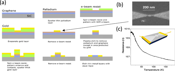
Figure 1. (a) Schematic of the graphene quantum dot fabrication process. (b) SEM image of the patterned metal mask used to fabricate the graphene quantum dot. (c) Resistance versus temperature of a graphene quantum dot bolometer.
Download figure:
Standard image High-resolution imageThe quantum dot forms a nano-constriction that opens a quantum confinement gap in graphene. As a result, the graphene resistance shows a strong temperature dependence, as high as 100 MΩ K−1 at temperatures below 10 K, due to thermal activation of the electronic current over the quantum confinement gap. When the graphene is irradiated, the electron temperature increases in the whole graphene area, the device resistance decreases and a photovoltage can be measured. The strong temperature dependence of the resistance is due to thermal activation of the electrical current over an energy barrier that is inversely proportional to the dot diameter [11]. This simple device design yields detectors with electrical responsivity as high as 1010 V W-1 and noise equivalent power below 2 × 10⁻¹⁶ W Hz−0.5 at 2.5 K [11, 12, 31]. These figures of merit are based on the absorbed power and the absorbed power can be measured directly from the bolometer current–voltage characteristics [11, 12].
We can assess whether the quantum dot bolometers are sufficiently sensitive for spectroscopy of monolayer samples by estimating the power absorbed by a monolayer of SMMs covering the graphene area. As an example, we consider the Fe4 complex [Fe4III(acac)6(Br-mp)2] with ground spin state S = 5 (Hacac = acetylacetonate, Br-mpH3 = Br-CH2-C(CH2OH)3) [32]. The energy spacing between ms = 4 and ms = 5 is equivalent to the energy of a 92.4 GHz photon (or 0.380 meV). Assuming that under continuous-wave irradiation the rate of photon absorption is limited by the relaxation time T1, we can estimate the absorbed power from a single SMM, P1M, as the ratio of the photon energy matching the energy level spacing to the relaxation time. By using T1 ∼ 1 μs (at 4.3 K) [32], we find P1M ∼ 6 × 10⁻¹⁷ W. If a monolayer of SMMs covers the whole graphene area, about 20 μm2 for the smallest bowties, for an approximate SMM size of 1 nm, we estimate 2 × 10⁷ SMMs covering the graphene and absorbing about 1.2 nW. This power is much higher (by at least two orders of magnitude) than the smallest absorbed power that we can measure with the graphene quantum dots [11, 12, 31], therefore power absorption from monolayer SMMs will cause a change in the power absorbed by the graphene quantum dots that should be easily measurable.
2. Experimental results
2.1. Deposition of single molecule magnets
Successful deposition of SMMs on substrates (and specifically on graphene) is a key milestone toward the goal to use graphene quantum dots for in situ spectroscopy of monolayer SMMs. Previous work on the deposition of SMMs on surfaces mainly used dropcasting [26, 28] or evaporation methods [29, 33, 34]. A common challenge of these deposition methods is the need to preserve the chemical structure of the molecule during the process. Dropcasting is done from a solution of SMMs in a solvent such as dichloromethane. Typically, this method does not provide samples with uniform thickness across the substrate and it very often causes so-called coffee-ring effects. Evaporation in vacuum yields better uniformity, but the SMM temperature needs to be carefully controlled, so that it is not raised above the decomposition temperature of the molecules. As an example, we describe our tests on deposition methods of a cobalt-ferrocene dimer (CFD), with formula [Br2Co(P(C6H5)2C5H4)Fe], or [Co(dppf)Br2]. The spin S = 3/2 of this SMM is due to three unpaired electrons on the Co2+ ions. Although there are some previous studies of its bulk properties [35], this CFD SMM has not yet been characterized as thin layers. We tested three deposition methods. The first method was based on a modified Langmuir–Schaefer deposition and tested using few-layer graphene (FLG) as a deposition surface [36]. Briefly, FLG was first deposited on a silicon substrate coated with SiO2 from a suspension of graphene nanosheets in N-methyl-2-pyrrolidone [36]. The FLG-coated substrate was then immersed in a container filled with deionized water. A solution of CFD in chloroform was then carefully deposited onto the water and formed a film on the surface of the water. Two movable barriers were used to compress the molecules into a layer, the water was carefully pumped out and the layer of molecules was collected on the FLG-coated substrate. Figure 2(b) shows an AFM image of the molecules deposited with this method. This deposition method could achieve good uniformity on large-area substrates, but the deposited molecules lumped into large (a few hundreds of nm in size) crystals. Although the HF-EPR spectrum of the deposited molecules (shown in figure 2(a)) had resonance peaks close to the frequencies expected for bulk samples, the peaks were broader and the noise was higher.
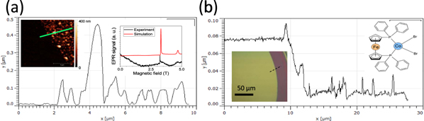
Figure 2. (a) AFM image (inset) and topography profile (measured along the green line) of [Co(dppf)Br2] deposited on few-layer graphene via Langmuir–Schaefer deposition. Inset: Measured (black) and simulated (red) HF-EPR spectra of the deposited molecules. (b) AFM topography profile and optical image (inset) of SMM [Co(dppf)Br2] deposited on SiO2 via sublimation, with a 4 h deposition at 215 °C. The images show the edge between the SMM region and the substrate.
Download figure:
Standard image High-resolution imageAs discussed below, the presence of water likely affected the molecules at the surface of the crystal. Moreover, due to the sample morphology, mainly the bulk of the crystals rather than the surface contributed to the EPR signal. Basically, an accurate SMM characterization of surface molecules was not possible with this deposition method. The second method involved dropcasting dichloromethane solutions of different concentrations of this SMM. We found that this molecule was strongly affected by the presence of moisture and did not retain the Raman and UV-visible spectral signatures that we had measured for bulk samples. When the dropcast was done in a glovebox with dry nitrogen, the molecule retained its spectral features but its distribution on the substrates was non-uniform and showed 'coffee ring' effects.
The third deposition method was evaporation of the molecules in vacuum (10−5 Torr), using a dedicated vacuum chamber that allowed control of the temperature of the molecules. Figure 2(b) shows a sample with a 80 nm layer of CFD SMMs on a Si/SiO2 substrate, obtained after a 4 h deposition at 215 °C. For depositions below 220 °C, the SMMs preserved their Raman and UV-visible spectral signatures, suggesting that thermal evaporation may be the best method to obtain a uniform, thin layer of CFD SMMs.
Tests of depositions to obtain thinner layers are underway.
2.2. Photodetection and its magnetic field dependence
Our previous work on graphene hot-electron bolometers was based on photodetection without a magnetic field applied. However, HF-EPR requires characterization with magnetic field of up to several Teslas. Since the conductance of graphene can be affected by magnetic field (e.g. due to the formation of Landau levels [37–39]), it is important to test the effect of an applied magnetic field on the photoresponse of graphene quantum dot bolometers. Figure 3(a) shows the current–voltage characteristics (source-drain current as a function of source-drain voltage) of a graphene quantum dot bolometer with the radiation off (black curve) and irradiated with a continuous wave source at 100 GHz (green), without an applied magnetic field, at a temperature of 15 K. We note that the current–voltage characteristic is nonlinear due to heating effects from the bias current [11]. The power absorbed from the THz source is about 2.4 pW, showing that even at temperatures above 10 K, the bolometers can resolve values of absorbed power that are much smaller than the power absorbed by a SMM monolayer. Although the bolometer responsivity drops when the operating temperature increases, the value is still as high as 108 V W-1 at 80 K for small diameter (less than 50 nm) quantum dots [11]. When an external magnetic field is applied, the response does not change noticeably, up to the maximum field of 7 T (red curve). Figure 3(b) shows a signal proportional to the source-drain current measured with a lock-in technique, using irradiation through a chopper at 11 Hz, at a fixed source-drain voltage. In the red regions the radiation was fully blocked and the signal dropped. The measurements show that the photoresponse at 15 K is almost independent of the magnetic field up to 7 T. We note that while the field was ramped there were small changes of the sample temperature, within 75 mK. Such variations of the sample temperature did not cause any measurable change of the sample resistance (the temperature had to be changed by at least 100 mK to cause a measurable change of sample current). We tested the graphene quantum dot bolometers in a cryostat with a larger maximum field and at lower temperature (1.5 K) and found that the photoresponse is independent of the magnetic field up to 15 T [40]. This can be understood by considering that the quantum confinement gap in the dots is dominated by the charging energy, which does not depend on the magnetic field, making the graphene quantum dot bolometers ideal detectors for HF-EPR measurements.

Figure 3. (a) Current–voltage characteristic of a graphene quantum dot with radiation off (black) and irradiated at 100 GHz at zero magnetic field (green) and at 7 T (red). The curves with radiation ON at zero field and 7 T overlap and cannot be easily distinguished. The absorbed power is 2.4 pW. (b) Lock-in signal of the THz response at VSD = 1 V an T = 15 K, with chopper frequency of 11 Hz, (black) and sample temperature (blue) as a function of magnetic field, applied perpendicular to the SiC substrate (above 3 T the magnetic field is ramped at a slower rate and the temperature is more stable). The radiation is completely blocked in the red shaded regions and the signal drops.
Download figure:
Standard image High-resolution imageTo test the operation of graphene quantum dots for HF-EPR spectroscopy, we decorated the graphene with powder of Mn12, as shown in the optical image in figure 4(b), and we measured the SMM absorption as a function of frequency at zero magnetic field. Here the powder was simply dropped dry (not in solution) on the samples. Mn12 is the archetypal SMM and its properties have been widely studied. Mn12 has a ground state spin of S = 10. The frequency domain magnetic resonance (FDMR) spectrum of a bulk sample in figure 4(a) shows absorption peaks for transitions between the lowest energy levels, ∣ms ∣ = 10 and ∣ms ∣ = 9 and ∣ms ∣ = 9 and ∣ms ∣ = 8, occurring in the range 200–350 GHz. Similar absorption peaks are measured with the decorated graphene quantum dot bolometer, using the ratio of the photoresponse measured from the bolometer decorated with molecules to the photoresponse measured from the bare bolometer, without molecules. Unfortunately, the THz source used for the measurements in figure 4(b) was a backward wave oscillator (quasi-optical source QS2, Microtech Instruments Inc.), that was not suitable for a careful analysis of the lineshapes [41], but these resonant absorption peaks could clearly be measured, even for this much smaller amount (compared to the measurements of figure 5(a)) of SMMs. We can roughly estimate the number of molecules in the cluster overlapping with the graphene bolometer from the optical image in figure 4(b). The area of the cluster is about 10 × 5 μm2. We measured the height of clusters with similar size by using SEM imaging and found that it was always below one micrometer, typically a few hundreds of nanometers. We use the upper bound of one micrometer for the height of the cluster to obtain a cluster volume of 5 × 10⁻¹⁷m3. By assuming that the size of the Mn12 SMM is about 1.5 nm, yielding a volume of 3.4 × 10⁻²⁷ m3 for a single SMM, we estimate that the cluster contains less than 1.5 × 10¹⁰ SMMs. We note that the bolometer used in this measurement is not coupled to an antenna. There is a large impedance mismatch between the high resistance of the bolometer and the characteristic impedance of free space, therefore the coupling between the incident radiation and the detector (decorated with SMMs or bare) is very weak. The signal can be enhanced by a few orders of magnitude by using an antenna to reduce the impedance mismatch and to focus the THz radiation on the detector. Nevertheless, even without optimizing the coupling to the THz radiation, we estimate that the bolometer can detect less than 1.5 × 10⁹ spins (if we take in account a signal-to-noise ratio of about 10) at 4 K. The Mn12 powder did not stay on the sample when a magnetic field was applied, therefore measurements in magnetic field will require different deposition methods, where the Mn12 molecules are anchored to the surface.

Figure 4. (a) HF-EPR Absorption spectra of a SMM-Mn12 powder pellet as a function of the radiation frequency with no magnetic field applied, using a Golay cell detector. The pellet is about 5 mm wide and 1 mm thick. The spectra show the transitions between different ms states at different temperatures and are normalized to the spectrum measured at 40 K. (b) Absorption spectrum of Mn12 powder deposited on the graphene quantum dot bolometers. The spectrum is measured using the ratio of the graphene bolometer lock-in response to THz radiation with and without powder, respectively. The location of the bolometer is indicated by the green bowtie.
Download figure:
Standard image High-resolution image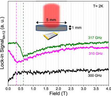
Figure 5. Absorption as a function of magnetic field for a Mn12 pellet, measured at different frequencies using the graphene quantum dot bolometer. The dashed lines represent the absorption peak values predicted from calculations.
Download figure:
Standard image High-resolution image
However, since previous work showed that Mn12 SMMs are not suitable for surface deposition [28], in future experiments we will focus on different SMMs, with smaller size and possibly with smaller deformation when deposited on a substrate, similar to those discussed in the previous section. We nevertheless performed test measurements of Mn12 powder pellets in magnetic field using the graphene bolometer. Figure 5 shows three absorption spectra as a function of magnetic field, at fixed frequencies, 300 GHz (where the absorption peak occurs at zero magnetic field), 310 GHz and 317 GHz, respectively. The absorption peaks for the ms ±10 to ms ± 9 transition occur at values of magnetic fields that match the peak values calculated with EasySpin, a MATLAB-based computational package [42]. The values obtained from the simulations are indicated by the vertical dashed lines in figure 5.
3. Discussion
As mentioned earlier, the open design of the graphene quantum dot bolometers allows the direct deposition of molecules on the surface of the graphene for HF-EPR spectroscopy. Our tests with Mn12 powder show that, at frequencies corresponding to resonant absorption from the molecules, the bolometer photoresponse decreases. This means that the current through the graphene quantum dot decreases. This change in photoresponse indicates that the power absorbed by the molecules is not transferred to the graphene electrons, namely, for frequencies matching resonant absorption from the molecules, the graphene electrons are partially shielded from the THz source, they absorb less power, the resistance decreases and the bolometer current also decreases. This is the basic mechanism that will allow in situ spectroscopy of the molecules to extract important characteristic parameters of the molecules on the surface, including the zero-field splitting parameter and the barrier height, the orientation of the molecular spin with respect to the magnetic field, the ms energy level spacing and the strain-induced broadening of the resonant peaks. These parameters can be extracted by fitting the measured spectra to EPR models.
Notably, these sensitive bolometers can already detect fewer than 109 spins, without any design optimization. Future work will focus on pushing the sensitivity limits of this technique by using on-chip antennas and Si lenses to focus the THz radiation and improve its coupling to the bolometer and to the SMMs. Resonant absorption and analysis of the peak lineshapes will be done either at a fixed frequency, by sweeping the magnetic field, or at a fixed magnetic field, by sweeping the frequency. The characterization method proposed here can be applied to any type of SMM, once the surface deposition technique has been optimized. We envision that, for molecules weakly interacting with the graphene surface, the bolometer can be used multiple times after washing away the molecules and annealing the device.
4. Conclusions
Epitaxial graphene quantum dot hot-electron bolometers are ideal tools to characterize and study SMMs on surfaces, with the unique advantage to provide in situ measurements and extract information on the interactions between the molecules and the graphene substrate. The substrate can be tailored by coating the graphene with other materials. This diagnostic tool can allow a fast characterization of SMMs and accelerate progress in the discovery of the specific substrates that can enhance their magnetic properties. Our proposed heterostructures of graphene and SMMs are also potentially a novel platform for molecular spintronics that is scalable since the quantum dots are made from large-area epitaxial graphene grown on silicon carbide. Future designs will include side gates to add device functionality to the graphene quantum dots and potentially increase their bolometric responsivity by tuning the thermal activation barrier for the electrical current through the dot.
Acknowledgments
This work was supported by the US Office of Naval Research (N00014-16-1-2674 and DURIP N00014-17-1-2436) and the NSF (ECCS-1610953). Research at NRL was supported by the Office of Naval Research. Research at CEITEC was supported by the Ministry of Education, Youth and Sports of the Czech Republic under the project CEITEC 2020 (LQ1601), by MŠMT Inter-Excellence (LTAUSA19060, 2020-2022), by CEITEC Nano Research Infrastructure (ID LM2015041, MEYS CR, 2016-2019), CEITEC Brno University of Technology, and by the ERC, under the European Union's Horizon 2020 research and innovation programme (GA No. 714850). Furthermore, support through DFG: INST 41/863, NE1900/2-1, SPP1601 NE1900/3-2 and SL104/3-2 is greatly appreciated together with Baden-Württemberg Stiftung (Elite program for Postdocs), as well as EPSRC (EP/G004757) and EU FET-OPEN (GA No. 767227). I N also acknowledges the financial support from the Department of Inorganic Chemistry, Palacky University, in Olomouc, Czech Republic and the Czech Science Foundation (GAČR) via Grant No. 19-01536S. The authors appreciated useful discussions with Dominik Bloos (University of Stuttgart) and ShangDa Jiang (Beijing University). J H acknowledges Dmytro Kostiuk and Peter Šiffalovič (Slovak Academy of Sciences) for the help with Langmuir–Schaefer sample deposition.