
Abstract
We present a 5 mm wide ten emitter dual-wavelength Y-branch DBR laser diode array emitting at 785 nm with an output power of 1 W at both wavelengths. The two emission wavelengths are individually addressable. The emitters are spectrally stabilized by deeply etched 10th order Distributed Bragg Reflector (DBR) gratings, realized by e-beam lithography. The wavelengths at 1 W output power are 784.0 nm and 784.6 nm. The spectral width of the emission of the individual emitters is below 20 pm. The spectral width of the array at 1 W is less than 60 pm caused by a variation in emission wavelength of about 40 pm of the individual emitters operating at one wavelength. The ten individual emitters reach an optical output power of 100 mW with minor variation of only 5 mW.
Export citation and abstract BibTeX RIS

Original content from this work may be used under the terms of the Creative Commons Attribution 4.0 licence. Any further distribution of this work must maintain attribution to the author(s) and the title of the work, journal citation and DOI.
1. Introduction
Wavelength stabilized laser diode arrays are needed for several applications in research and industry. Laser diode arrays in external cavity configurations are for example used for fundamental physics measurements [1] or pumping of alkali-vapor lasers [2]. Wavelength division multiplexing in optical communication networks is realized by distributed feedback laser arrays [3, 4]. With stabilized wavelength and narrow linewidth laser arrays are suitable for spectroscopic applications, such as Raman spectroscopy.
Raman spectroscopy is a well-established analytical tool for the identification of molecules, where 785 nm is one of the most common excitation wavelengths [5]. There are two challenges applying Raman spectroscopy on real-world samples. Firstly, laser induced fluorescence and ambient light can masked the weak Raman signals. Secondly, measuring heterogeneous samples, the selection of a significant spot with an adequate spotsize can essentially influence the result of the measurement [6].
For heterogeneous samples, i.e. samples with an inhomogenoeus distribution of different constituents, e.g. biological material or soil, a potential solution is the increase of the excitation spot size. To achieve power densities comparable to smaller spot sizes, here high power lasers with excellent beam quality are required. Besides that, the optical properties of the used Raman spectrometer limit the collection area of Raman photons. This is why a multi-spot exciation can be favorable. This way, the exciation area on the sample can be increased while assuring apropriate power densities and enabling the sufficient collection of the Raman photons. A general drawback of increasing the excation area could be the increase of disturbing fluorescence.
To overcome this, shifted excitation Raman difference spectroscopy (SERDS) can be applied, which uses two slightly different wavelengths for the generation of two slightly shifted Raman spectra. While the Raman lines follow the change of the excitation wavelength, the disturbing background remains spectrally unchanged. If now the two spectra are substracted, disturbing background interferences and fixed pattern noise can be removed from the Raman spectrum [7, 8]. Different light sources for SERDS are known, e.g. optical parametric oscillators [9], temperature tuned diode lasers [10] or dual-laser sources using Volume Bragg Grating technology for wavelength stabilization [11]. A more compact and robust excitation light source for SERDS is the dual-wavelength DBR Y-branch laser diode [12, 13]. At an emission wavelength of 785 nm, devices are reported with optical output powers of >200 mW and a spectral width below 20 pm.
A potential light source suitable for multi-spot SERDS would be an array of dual-wavelength Y-branch DBR lasers. Such a light source would have to meet the general requirements for Raman spectroscopy for the measurement of solids and liquids. The spectral width of the emission should be smaller than 1 cm−1 [14], i.e. ≤60 pm at 785 nm. For individual emitters, this was already shown in the above-mentioned reference. For the investigation with SERDS the spectral distance Δλ of the two excitation wavelengths should be about 10 cm−1 (0.6 nm) close to the spectral width of the Raman bands under study [14]. Besides the spectral requirements, the output power over the array should be homogenously distributed over the emitters.
In this work, a 5 mm wide edge-emitting array of ten dual-wavelength Y-branch DBR laser diodes will be presented. The array provides an overall optical output power of 1 W. To the best of our knowledge, this is the first dual-wavelength array with output powers in the watt range.
In the following, the material parameters, the fabrication process as well as the lateral design will be presented. The electro-optical and the spectral properties for the overall array as well as the behaviour of the individual emitters will be shown and discussed.
2. Vertical and lateral laser structure
The vertical layer structure of the monolithic dual-wavelength Y-branch DBR laser diode array is grown on 3-inch GaAs wafers using Metalorganic Vapor Phase Epitaxy (MOVPE) and is depicted in figure 1.

Figure 1. Scheme of the vertical layer structure for the 785 nm Y-branch laser diode array.
Download figure:
Standard image High-resolution imageThe active zone consists of a 14 nm thick GaAsP single quantum well (SQW), which is embedded in a 1 μm thick AlGaAs waveguide. The waveguide comprises 500 μm thick Al0.65Ga0.35As n- and p-waveguide layers and is surrounded by 1000 μm thick Al0.7Ga0.3As n- and p-cladding layers. The structure is similar to the one presented in [15].
For the determination of the material properties, uncoated devices with a stripe width of 100 μm with different lengths are tested in pulsed operation (1 kHz, 1 μs).
For 1 mm long devices the measured threshold current is Ith = 230 mA and the slope efficiency is S = 0.67 W A−1, i.e. a differential efficiency ηD = 0.85. The characteristic temperature of the threshold current is T0 = 140 K. The length dependencies of the threshold current and the slope efficiency are used to calculate the material parameters. An internal efficiency ηi of 0.91 and internal losses of 0.91 cm−1 are determined. The calculated values of the transparency current density jTR and the threshold current for devices with infinite length j∞ are 115 A cm−2 and 122 A cm−2, respectively. A modal gain coefficient Гg0 of 18 cm−1 is determined. The determined material parameters illustrate the quality of the grown material and its suitability for processing laser devices.
Figure 2 shows the measured vertical far field distribution for the described layer structure. The distribution has a Gaussian like shape and the full vertical far field angle at half maximum (FWHM) is ΘFWHM = 29°. 95% of the power is emitted within an angle of Θ95% = 54°.
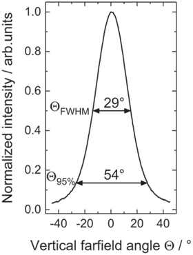
Figure 2. Measured vertical far field distribution of the structure for the 785 nm Y-branch laser diode array.
Download figure:
Standard image High-resolution imageThe material was processed in a full wafer process using an i-line wafer stepper and electron beam lithography for manufacturing the grating structures.
The array consists of ten dual-wavelength Y-branch DBR diode lasers as shown in the scheme in figure 3. The device length is LArray = 3 mm and the device width is wArray = 5 mm. The pitch of the single emitters is 500 μm adapted to standard micro lens arrays for future applications.

Figure 3. Photo (top view) of the dual-wavelength Y-branch DBR laser diode array with an overlaying schematic drawing of the lateral design of the array.
Download figure:
Standard image High-resolution imageThe lateral waveguide design is the same as for single dual-wavelength Y-branch DBR laser diodes already presented in [16]. Each individual laser diode comprises a left (L) and a right (R) 2000 μm long sine-shaped S-bend ridge waveguide (RW) branch. The RW branches are coupled into a common 500 μm long straight RW output section. The RW width is 2.2 μm. In contrast to the devices reported in [16], the deeply etched DBR surface gratings at the back facet are manufactured with electron beam lithography. The tapered 10th order DBR surface gratings form the back reflective mirrors (indicated by dotted lines in figure 3). The lateral distance of the two 500 μm long DBR gratings of one laser diode is 80 μm. The grating width is 10 μm at the back facet and narrows to 2.2 μm along the grating to match the RW width. A more detailed description of the same DBR grating design can be found in [17]. The grating periods of the DBR gratings of the two branches of a single emitter are different, thereby providing two different emission wavelengths. The two design wavelengths of the array are 784.0 nm and 784.6 nm to provide the mentioned spectral distance of 10 cm−1 (0.6 nm) and to match standard Raman filters.
The lengths of the electrical contacts differ from the lengths of the waveguide parts described above. The branches have a contact length CBranches = 1320 μm, the coupler section CY = 380 μm (Y-section) and the output section COut = 690 μm.
As illustrated in figure 3, all laser diodes D01 to D10 share the contact COut (colored in orange) at the front facet and the Y-section contact CY (colored in turquoise). To minimize the number of contacts, adjacent branches of two laser diodes have a common contact, CBranches (colored in yellow and grey). For that reason, the DBR grating periods of the laser branches, which share a contact CBranches, are chosen to be the same. Hence, adjacent branches from two diodes with a common contact produce the same emission wavelength. Altogether 13 contacts are used for the operation of the device. Please note, that in contrast to the underlying contact layers, the top layer of the metallization of COut, CY and CBranches is interrupted between the single emitters, which appears as dark lines between the emitters of the array in the photo of figure 3.
At the front facet a 5% anti-reflective coating is applied, while the back facet is anti-reflection coated. The array is soldered p-side up to a copper tungsten (CuW) heat spreader, which is mounted on a 25 mm × 25 mm conduction-cooled package (CCP).
3. Electro-optical and spectral properties
In the following, the electro-optical and spectral properties of the array will be presented, while all emitters having one wavelength are operated simultaneously. All measurements were done at a heat sink temperature of 25 °C. For single Y-branch DBR laser diodes a current of 35 mA through the output section and a grounded Y-section has proven to result in the best spectral behavior for this vertical and lateral laser diode design while one of the RW branches is used as pumping region. For this reason, a current of IOut = 350 mA was applied to the common output section and the Y-section was grounded for all measurements. For this reason, the current at which lasing starts will be named ILas in the following as it differs from the threshold current Ith because there are parts of the resonator which are unpumped or pumped at constant current.
3.1. Array characterization
Figure 4 presents the power-voltage-current characteristics of the array. The solid and dashed lines belong to the simultaneously operated branches with emission wavelength λ1 and λ2, respectively.
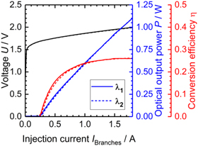
Figure 4. Power-voltage-current characteristics of the dual-wavelength Y-branch DBR laser diode array at T = 25 °C with IOut = 350 mA and Y-section grounded. Solid lines refer to emission wavelength λ1 and dashed lines to λ2.
Download figure:
Standard image High-resolution imageLasing starts at an injection current IBranches = ILas = (260 ± 20) mA for both λ1 and λ2. The slope efficiency is S = (0.70 ± 0.04) W/A. The maximum conversion efficiency is η = 0.26 measured at IBranches = 1.8 A, which includes both the electrical power of the operated branches as well as the common output section. For both wavelengths λ1 and λ2 an optical output power of PBranches = 1 W is reached at IBranches = 1.6 A. As it can be seen from figure 4 no roll-over can be observed.
Figure 5 illustrates the spectral behavior of the overall array. The separately normalized spectra of both emission wavelengths are plotted as a false color diagram over the injection current. The spectra were recorded using a DEMON double echelle monochromator from LTB Berlin, which provides a spectral resolution of about 11 pm at 785 nm. Please note that the two different emission wavelengths λ1 and λ2 are not operated at the same time, but are combined to a single spectral map for better visualization.
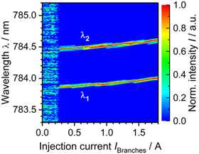
Figure 5. Spectral behaviour of the dual-wavelength Y-branch DBR laser diode array at T = 25 °C with IOut = 350 mA and Y-section grounded.
Download figure:
Standard image High-resolution imageAt lasing current ILas the peak wavelengths are λ1 = 783.85 nm and λ2 = 784.47 nm. The difference between the two wavelength amounts to Δλ = 0.62 nm. With increasing injection current IBranches the emission wavelengths shift towards longer wavelengths. Over the whole operating range, the emission width of both emission wavelengths is narrow. The spectral distance Δλ between the two peak emission wavelengths of λ1 and λ2 varies between Δλ = 0.59 nm and Δλ = 0.63 nm over the whole operating range. The averaged spectral distance  between both peak emission wavelengths is 0.61 nm.
Figure 6 shows the two spectra at both emission wavelengths at PBranches = 1 W. Here, the maxima of the two wavelengths are λ1 = 783.98 nm and λ2 = 784.58 nm, which is in good agreement with the aimed design wavelengths.
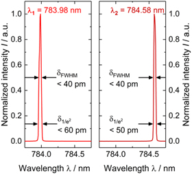
Figure 6. Spectra of the dual-wavelength Y-branch DBR laser diode array at an optical output power of 1 W. Single spectra of emission wavelengths λ1 and λ2 from figure 5 at an injection current of IBranches = 1.6 A and Iout = 350 mA at T = 25 °C, Y-section grounded.
Download figure:
Standard image High-resolution imageAt full width half maximum (FWHM) the spectral width δFWHM is smaller than 40 pm for λ1 and λ2. At a level of 1/e2 the spectral widths of λ1 and λ2 are δ1/e2 < 60 pm and δ1/e2 < 50 pm, respectively. Hereby, the array is suited for Raman spectroscopy as an excitation light source in the watt range. Furthermore, the spectral distance of λ1 and λ2 with Δλ = 0.60 nm (10 cm−1) is well suited for SERDS.
In addition to the shown suitability of the overall array characteristics, a multi-spot excitation light source needs to have individual emitters having comparable output powers. In the following section, the emission of the individual emitters was characterized while all emitters were operated at the same time.
3.2. Emitter characterization
For the electro-optical and spectral characterization of each individual emitter when all emitters are operated simultaneously a lens (f = 3.1 mm, numerical aperture NA = 0.68) was used to separate the laser spots of the emitters. The chosen lens collimates a selected laser spot while the neighboring spots are refracted in a way that they do not reach the power detector or the integrating sphere connected to the spectrometer. Figure 7 shows the power-current characteristic for each individual emitter. As can be seen from the figure, the optical output power behaves similar for all emitters. Please note, that for the emitter characterization the approximation is made that the injection current splits equally between the individual emitters.
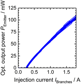
Figure 7. Power-current characteristics of all individual emitters of the dual-wavelength Y-branch DBR laser diode array at T = 25 °C with IOut = 350 mA, Y-section grounded.
Download figure:
Standard image High-resolution imageAs expected from the lasing current ILas for the array, the lasing currents of the individual emitters are around (26.0 ± 0.5) mA per emitter. Figure 8 a shows the lasing current for the individual emitters. The lasing current varies between (23.5 ± 0.5) mA and (27.5 ± 0.5) mA. This variation is mainly caused by fabrication uncertainty of the lateral waveguide structure and the variation in the length of the wire bonds and conducting paths on the circuit boards. The different resistances of the leads cause a slightly inhomogeneous current distribution between the emitters. In the future, the design of the circuit board and the control of the wire bond length could be enhanced. For both emission wavelengths, the sum of the ten individually measured lasing currents of the emitters is in good agreement with the array lasing current of (260 ± 20) mA and amounts to 253.5 mA for λ1 and 267 mA for λ2.
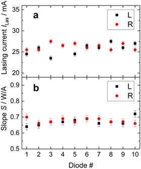
Figure 8. Lasing current ILas (a) and slope S (b) of all individual emitters of the dual-wavelength Y-branch DBR laser diode array (T = 25 °C, IOut = 350 mA, Y-section grounded).
Download figure:
Standard image High-resolution imageFigure 8(b) presents the slope efficiencies S of the individual emitters. The slope efficiencies S for each emitter were determined in the range from 0.5 A ≤ IBranches ≤ 1.2 A.
The slope efficiency S varies over the array only marginal and amounts in average to (0.68 ± 0.02) W/A, which is in good agreement with the array characterization.
Figure 9 shows an exemplary spectral map of the individual emitter D05-L, which is representative for all other emitters. With increasing injection current IBranches the maximum of the emission wavelength shifts towards longer wavelengths. The spectrum is single mode over the whole operating range. Some mode hops can be seen, where the maximum of the emission wavelength jumps to a shorter wavelength before increasing again. This behavior is typical for a DBR laser diode.
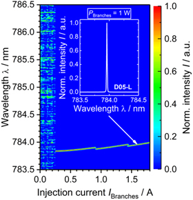
Figure 9. Spectral behaviour of emitter D05-L of the dual-wavelength Y-branch DBR laser diode array array at T = 25 °C with IOut = 350 mA, Y-section grounded. The inset shows the spectrum of D05-L at an optical output power of 1W of the array.
Download figure:
Standard image High-resolution imageThe sizes of the mode hops of about 30 pm are in good agreement with the resonator length of 3 mm, when assuming a Fabry–Perot resonator (with effective index neff = 3.5). The spectral width for the individual emitters at an optical output power of the array of PBranches = 1 W was measured to be 11 pm. This value is limited by the spectral resolution of about 11 pm of the used spectrometer.
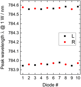
The peak emission wavelengths of the individual emitters at the optical output power of the array of PBranches = 1 W are depicted in figure 10. For the emitters with λ1 the peak wavelength varies between (783.94 ± 0.01) nm and (783.98 ± 0.01) nm. For the emitters with λ2 the peak wavelength varies between (784.56 ± 0.01) nm and (784.58 ± 0.01) nm. The average value of all emitters with λ1 is 783.96 nm and 784.57 nm for λ2. Considering the mentioned narrow spectral width of the individual emitters, the variation in peak wavelength of the emitters is in good agreement with the measured spectra of the overall array. The variation in wavelength of the individual emitters is 40 pm for λ1 and 20 pm for λ2. Together with a spectral width at 1/e2-level of about 20 pm for the single emitters, this leads to the overall spectral width of the array of δ1/e2 < 60 pm and δ1/e2 < 50 pm for λ1 and λ2, respectively. There is no indication of an emitter position dependence regarding the spectral characteristics. The measured temperature dependence of the DBR grating emission wavelength for single Y-branch DBR laser diodes is 0.05 nm K−1. Therefore, the variation in emission wavelength of 40 pm and 20 pm indicates a variation in temperature along the array of less than 1 K and a homogenous temperature distribution along the array can be assumed. As mentioned in [18] wavelength uncertainty is caused by random optical phases at the front facets. The measured peak wavelength variations along the Y-branch DBR laser diode array are about the size of a mode hop. The fabrication precision of the definition of the cavity length is limited, which explains the measured variations in wavelength.
Figure 10. Peak wavelenghts of the individual emitters of the dual-wavelength Y-branch DBR laser diode array at an optical output power of 1W of the array array at T = 25 °C with IOut = 350 mA, Y-section grounded.
Download figure:
Standard image High-resolution image
On the basis of successful lifetime tests of single Y-branch DBR lasers diodes of more than 1,000 h per RW branch at an optical output power of about 100 mW, we expect similar lifetimes of the array at 1 W optical output power. Lifetime tests of the array at 1 W optical output power have been started recently.
4. Conclusion
A 5 mm wide array of ten dual-wavelength Y-branch DBR laser diodes at 785 nm, which provides an optical output power of 1 W, was demonstrated. Lasing starts at a current of 260 mA. The slope efficiency is 0.7 W A−1 and the maximum conversion efficiency is 0.26. All individual emitters show similar data features in lasing current, slope efficiency and optical output power. The spectra of all individual emitters are single mode and exhibit similar spectral characteristics. This leads to the single mode spectra of the overall array at 1 W optical output power with a spectral width of less than 60 pm at 1/e2-level. The array is suitable as a multi-spot excitation light source for SERDS.
Acknowledgments
This work is realized within the project RaMBo (Raman Messsystem zur ortsspezifischen Bodenanalytik) within the consortium I4S (Intelligence for Soil) within the funding measure BonaRes (Soil as a Sustainable Resource for the Bioeconomy). The authors gratefully acknowledge the financial support by the Federal Ministry of Education and Research (BMBF) under contract 031A564C. This work was partly funded by the German Federal Ministry of Education and Research under the project reference number 16FMD02 (Research Fab Microelectronics Germany - FMD). We like to thank all involved colleagues at Ferdinand-Braun-Institut in the process technology department, in the optoelectronics department as well as in the mounting and assembly department.
Data availability statement
The data that support the findings of this study are available upon reasonable request from the authors.