
Abstract
Nanoscale characterization techniques are fundamental to continue increasing the performance and miniaturization of consumer electronics. Among all the available techniques, Kelvin-probe force microscopy (KPFM) provides nanoscale maps of the local work function, a paramount property related to many chemical and physical surface phenomena. For this reason, this technique has being extremely employed in the semiconductor industry, and now is becoming more and more important in the growing field of 2D materials, providing information about the electronic properties, the number of layers, and even the morphology of the samples. However, although all the collective efforts from the community, proper calibration of the technique to obtain reliable and consistent work-function values is still challenging. Here we show a calibration method that improves on current procedures by reducing the uncertainty. In particular, it allows grading probes more easily, thus being a tool to calibrate and to judge calibration in itself. The calibration method is applied to optimize Pt-coated probes, which are then used to characterize the work function of a 2D material, i.e. graphite flakes. The results demonstrate that the metallic probes are stable over time and exposure to high humidity levels, and that the calibration allows comparing measurements taken with several different probes on different samples, thus completely fulfilling the requirement of a good calibration method.
Export citation and abstract BibTeX RIS

Original content from this work may be used under the terms of the Creative Commons Attribution 4.0 licence. Any further distribution of this work must maintain attribution to the author(s) and the title of the work, journal citation and DOI.
1. Introduction
Nanoscale characterisation techniques have become extemely popular in recent years as the size of electronic devices keeps shrinking, especially after the advent of low-dimensional materials. Among the quantities that are of interest to characterize materials and devices, the work-function,  (i.e. the minimum energy needed to remove an electorn from the Fermi level to a vacuum point immediately outside the surface) is of huge of importance, because it is related to many paramount chemical and physical surface phenomena, such as band-alignment at the interface, charge carrier injection, and also electronic transport properties [1–3]. To this end, Kelvin-probe force microscopy (KPFM), which is an advanced scanning probe microscopy technique, has attracted considerable attention in recent years. First proposed by Nonnenmacher et al [4] in 1991, KPFM enbales measuring the surface charge distribution, also known as contact potential difference,
  together with the topography of the sample with nanoscale resolution [4] (∼50 nm and ∼20 mV of spatial and electrical resolution for the contact potential difference and ∼10 nm of spatial resolution for the topography). Moreover, if the work function of the probe is measured, typically by calibrating it against a reference sample with known work function, quantitative workfunction maps can be obtained directly from the
  For these reasons, mainly its versatility and high spatial and energetic resolutions, KPFM has been extensively employed in a variety of fields and applications such as thermionic emission in metals [5], semiconductor surface characterisation [6], photonic and electronic devices [7–9], and more recently, 2D materials [10–12], among others [13–15]. However, the obtention of reliable and repeatable values of the sample's work function is not that straight-forward as the
  is known to be strongly dependent on several parameters such as the measurement environment [16, 17], the tip geometry and material [18, 19], instrumentation effects [20], parasitic effects such as capacitive coupling [21, 22], as well as the chosen experimental parameters [23].
Although previous studies have worked towards tackling these issues, there are two essential requirements for the obtention of reliable sample's work function values that remain elusive: (1) the acquisition of the tip's work function with high precision, and (2) stable, artefact-free imaging conditions.
Regarding the first point, acquiring a precise value of the tip's work function requires the implementation of a calibration method providing the minimum uncertainty possible, and a stable reference surface with known work function. As an example, highly oriented pyrolytic graphite (HOPG) has been used as the preferred reference sample by many authors due to its low cost, easiness of manipulation, flatness and excellent electrical properties. However, the values obtained for different samples of HOPG present a large dispersion both in air and vacuum, with values ranging from 4.5 eV up to 5 eV [24–26]. Such a high work function dispersion, mainly attributed to surface contamination or inhomogeneities, makes this reference sample simply unreliable.
As for the second point considered, and as mentioned above, measurements can be disturbed by several factors such as: non reproducible scanning conditions (e.g. scanning in air atmosphere with changing humidity levels); poor feedback parameters (e.g. scanning too fast for the electrical fedback to respond to changes in the surface inmediately below the probe); tip-sample capacitive coupling due to the position of the probe with respect to the sample (e.g. scanning over metallic electrodes connecting the area of interest with the ground).
Here we propose a calibration protocol for KPFM in which the workfunction of the tip is obtained by linear fitting several  measurements instead of just one, like is typically done in previous calibration schemes. This is done by having several reference samples and applying different bias voltages to them, to increase/decrease the measured
  This approach reduces the uncertainty of the probe's work function, thus leading to better KPFM measurements.
To demonstrate the importance of calibration in KPFM, the discussion includes a study of the different sources of uncertainty affecting the measurement, showing that in most of the cases, without the calibration presented here, it was imposible to quantify the uncertainty.
In addition, an experimental case, using grafite flakes of different thicknesses, is presented to demonstrate that this calibration protocol indeed reduces the calibration uncertainty and allows combining the data from different probes.
2. Results and discussion
2.1. Scanning set-up and optimization of parameters
Prior to describing the developed calibration protocol, the experimental set-up and the scanning parameters are reviewed.
Here, single-pass phase modulated Kelvin probe microscopy (PM-KPFM) is used. As shown in figure 1(a), the probe oscillates over the surface in non-contact mode mapping the topography and the surface contact potential simoultaneously. In order to eliminate any offset due to the electrostatic interaction, all the samples in this study have been grounded, and unless indicated other way, imaging was performed in vacuum conditions (as recommended to achieve stable operation [27, 28]). Simoultaneous imaging of topography and contact potential is achieved by the presence of two separated feedback loops: one for tracking the mechanical interaction, i.e. the topography, and another one for the electrostatic interaction, i.e. the contact potential difference,  For the mechanical interaction, the cantilever is excited close to its resonance frequency, f0, and the mechanical feedback, consisting in a lock-in and a PID control, takes the laser signal, reflected from the cantilever, as an input to modify the Z piezo to lower/raise the probe and keep the oscillating amplitude constant. For the electrostatic signal, an oscillating voltage
  is applied to the probe at a frequency much smaller than the resonance, f', to avoid any interference between the signals, and the feedback loop used to minimize the electrical interaction, consisting on a second lock-in and another PID control, uses the demodulated signal from the first loop to lock at the frequencies f0 − f' and f0 + f' (see further details in the Methods section and [29]). The amplitude of this demodulated signal seen by the second lock-in is proportional to the gradient of the force and is used by the second PID loop to find the voltage
  that nullifies the electrostatic force, and which in principle is equal to the contact potential difference.

Figure 1. (a) Schematic diagram of the FM-KPFM mode employed here. Two different excitation signals, i.e. mechanical and electrical  are applied to the probe while scanning the sample. By compensating the electrostatic force stablished between tip-sample system with
  the contact potential difference signal of the different areas of the sample are acquired together with the topography. (b) Trace and retrace profiles of topography and VCPD
signals when crossing a step change. (c) Schematics of probe's movement when its position jumps from two different materials (i.e. Au and SiO2). (d) Measured X and Y positions and VCPD
when the probe moves following the pattern described in (c). (e) Effect of varying the amplitude of the oscillating voltage VAC
when imaging Pt and Au electrodes. (f) Effect of varying the excitation frequency f' when imaging a metallic electrode.
the contact potential difference signal of the different areas of the sample are acquired together with the topography. (b) Trace and retrace profiles of topography and VCPD
signals when crossing a step change. (c) Schematics of probe's movement when its position jumps from two different materials (i.e. Au and SiO2). (d) Measured X and Y positions and VCPD
when the probe moves following the pattern described in (c). (e) Effect of varying the amplitude of the oscillating voltage VAC
when imaging Pt and Au electrodes. (f) Effect of varying the excitation frequency f' when imaging a metallic electrode.
Download figure:
Standard image High-resolution imageAdditionally, it is important to mention that there are other methodologies also employed to measure the contact potential difference: the amplitude modulated Kelvin probe force microscopy (AM-KPFM), and the frequency modulated Kelvin probe force microscopy (FM-KPFM). FM-KPFM is similar to PM-KPFM, in the sense that it uses the force gradient to minimize the electrostatic interaction, but it requires a phase locked loop (PLL). In AM-KPFM, the chages induced in the amplitude of the cantilever at f' are used to compensate the electrostatic force. However, as highlighted by previous studies, as this method is proportional to the long-range electrostatic forces, the measured signal suffers from a strong averaging effect from the tip and the cantilever. Thuss resultsing in reduced accuracy and lateral resolution with respect to the PM-KPFM or the FM-KPFM schemes, justifying the selection of the PM-KPFM approach for the development of the work presented here [28, 30–32].
Then, using the setup described in figure 1(a), the obtention of quantitative reliable values of the work-function starts by optimising the measurement parameters. This aspect, which is many times overlooked, is critical in order to minimise the presence of artifacts.
The first step towards reliable calibrated KPFM consists in the selection of the right feedback parameters for the two operating feedback loops, i.e. mechanical and electrostatic. However, as the values of these parameters are highly dependent on the sample-probe system, and tend to change between scanning probe microscopy systems, we will not comment about PID optimization strategies here, see some advanced optimisation techniques in references: [33, 34]. But ultimately, as demonstrated by previous studies [35], the correct selection of feedback parameters leads to coinciding trace and retrace signals [35, 36]. Thus independently of the feedback parameters optimization algorithm used, imaging across a boundary where the sample under study presents a known step on both the topography and the VCPD , it's an excellent strategy for monitoring how good is the feedback. Here, an example is shown in figure 1(b), where imaging was performed using SPARK 350 probes purchased from NuNano, and the step change corresponds to the Au electrode from one of the reference samples (see Methods section) onto the SiO2 substrate. It can be seen that the feedback chosen to take the profiles shown in figure 1(b) was adequate, as both trace and retrace scans match each other for both topography and VCPD . Periodic oscillations, different curves for trace and retrace (in particular close to the step change), or spatial shift between the curves, are indicators of poorly chosen feedback parameters.
Nevertheless there is another scanning parameter, which tends to be underestimated in general, and that requires special attention when performing KPFM: the scan speed. In order to find the fastest scan speed possible, the same step change can be used. In this case, instead of scanning across the boundary, the tip is displaced almost instantaneously between specific locations of the substrate, jumping from the Au to the SiO2 substrate and back again, as depicted in figure 1(c). This process, if performed quickly enough, i.e.with less than ∼100 ms total displacement time, allows measuring the settling time which is how long it takes for the VCPD to reach stability [35]. In the particular case shown in figure 1(d), the changes in the position of the probe are depicted by blue curves, with X and Y represented by straight and dashed lines. It can be seen that each time the probe changes position it takes about ∼100 ms for the VCPD to settle to a constant value. This time constant of ∼100 ms, which might vary depending on the feedback loop and the capacitive coupling between the sample and the probe, determines the maximun scan speed, as the probe should at least stay 100 ms per pixel. In principle, one could drawn to the conclusion that less averaging time (i.e. higher bandwidth and thus integration of more noise) implies larger noise, while more averaging per pixel will lead to less noise, however in practice, things as thermal fluctuations affect electrical measurements that are averaged over long periods of time [37]. Therefore, there is an optimal amount of averaging, also known as integration time, beyond which further measurements just increase the uncertainty. This can be easily seen in an Allan deviation plot where the Allan deviation, a measurement of the noise in the averaged value, is represented against different number of averages, or diferent periods of integration time. An example of such plot is shown in figure 2(a), acquired with the same probes over the Au reference. It can be seen from the curve that averaging for periods longer than 250 ms leds to a significant increment in the noise. Thus, from this we can conclude that the optimal scanning speed is between 100 and 250 ms per pixel, and for all the measurements presented here a speed of 200 ms per pixel was used.
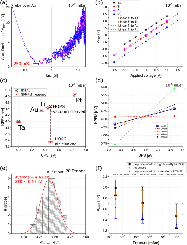
Figure 2. (a) Allan deviation plot showing the effect of different number of averages (i.e. varying the time constant of the electrical measurement), acquired by maintaining the probe stationary over the Au reference. (b) VCPD of metal thin films ( Pt, Ti, Au, and Ta) as a function of the bias voltage applied to the metal. (c) Work function of metal thin films (same as in (b)) and HOPG, KPFM measurements against UPS. (d) Measurement of Pt and Au work function using KPFM comparing probes with different coating thickness (e) Distribution of work function values for a batch of 20 nominally identical probes. (f) Effect of storage conditions where one set of probes is measured as-arrived (orange), and then compared against two set of probes, one kept in high humidity (black) and another one kept in low humidity conditions (blue) for one month.
Download figure:
Standard image High-resolution imageApart from the feedback and the scan speed, other two parameters that also affect the measured VCPD are the amplitude of the oscillating voltage VAC and the excitation frequency, f', of the electrical voltage applied to the probe.
A common assumption in KPFM experiments is that the applied voltage perfectly nullifies the electrostatic force between the probe and the sample. However, sometimes the presence of parasitic effects, e.g. capacitive coupling, could affect the measured signal. When accounting for this error in the electrical compensation (as it is shown in equation (8) in the Methods section with a first order correction), the measured VCPD depends on VAC , but not in the excitation frequency, meaning that the role of the voltage is more predominant. To demonstrate this, using the reference sample with Au and Pt electrodes (see the Methods section for fabrication details) the effect of VAC and f' were investigated and are shown in figures 1(e) and (f), respectively. It can be seen in figure 1(e) that the VCPD measured for Au and for Pt varies, tending to constant values for large voltages, as discussed in previous studies [30]. The difference between the two VCPD , should match that measured using UPS, and this happens only when the amplitude of the VAC is above 3V, thus indicating that the voltage should be kept at least higher than that value to minimize the error introduced by uncompensated electrostatic interaction. An important point should be noted here. While in principle, according to equation (8) a larger voltage will reduce the error, it is recommended to use the lowest excitation voltage posible, as large voltages can affect the samples under study [38, 39]. Thus having a reference material with two grounded electrodes of different materials helps identifying the optimal value of the VAC .
It can be seen in figure 1(f), that when measuring a single electrode while keeping the VAC amplitude constant but changing the excitation frequency f', the change in VCPD is monotonic, not tending to a constant value. However, the variation is much smaller than that produced by changes in the amplitude of VAC , and thus other reasons rather than uncertainty in the final measured work function should be taken into account when selecting the preferred frequency, e.g. to avoid cross-talk with the mechanical excitation of the probe [30] or to avoid interferrence with the electrical noise in the laboratory.
2.2. Calibration procedure
The calibration process proposed here consist in measuring four voltage-biased metallic thin films using KPFM and ultraviolet photoelectron spectroscopy (UPS). The UPS is assumed as calibrated, while the KPFM is the method being calibrated. While it is a calibration process similar to the ones followed in previous studies [16, 40, 41], it differs from [40, 41] in the fact that several metallic reference samples are used, while it is common practise to use only one, and from [16, 40] because a voltage is applied to the samples while performing KPFM. Adding more references for the calibration reduces the uncertainty in the probe's work function, and by biasing the sample, it is possible to obtain the final metal work function by a linear fitting, rather than from a single measurement, thus reducing even further the uncertainty of the calibration [42].
The first step consists then in measuring the work function of the metals using UPS. Results of this measurement are summarized in table 1 (see the Methods section for further details on the UPS). The four metals used for this study, Pt, Ti, Au, and Ta (see the fabrication details in the Methods section), were selected for having different work functions, and either resilience to oxidation, or because they develop a passivation oxide layers that stabilizes their surface. Then, in the next step, breaking the vacuum between the UPS and the KPFM, the samples were transferred into the KPFM system and put again under vacuum (∼10−6 mBar). After annealing at 300 °C, to clean the surface from contaminants adhered while the vacuum was broken, KPFM measurements were performed using SPARK 350 probes from NuNano. The optimization process described in the previous section was used prior to the measurements. The results of measuring the  under different bias voltages applied to the metallic thin films are summarized in figure 2(b), and the parameters of the linear fitting to the data can be seen in table 1. Each material follows a linear trend whose intercept is given by equation (4), i.e.
  Since
Since  is known through UPS, the intercept allows calculating the work function of the probe (shown in table 1), obtaining a value of ∼4.387 eV with a standard deviation of 14 meV. The advantage of this calibration protocol is that by using a least square fit to obtain the linear approximation for each material, the resulting probe's work function has less error than when using a single point per each reference material [42] (i.e. typically an error of 20–100 mV [26, 40]), thus obtaining a more accurate calibration of the probe work function.
Table 1. Results obtained for the materials measured in figure 2(b). From left to right: the intercept from the linear fitting, the associated error, the work function as measured using UPS, and the resulting work function of the probe by using equation (6).
| Material | Intercept [V] | Intercept standard error [V] | UPS [eV] ±0.01 eV |
 [eV] [eV] |
|---|---|---|---|---|
| Pt | −0.4341 | 0.007 | 4.84 | 4.4059 |
| Ti | −0.0385 | 0.008 | 4.43 | 4.3915 |
| Au | 0.0329 | 0.009 | 4.35 | 4.3829 |
| Ta | 0.3665 | 0.003 | 4.00 | 4.3665 |
The calibration protocol proposed here was then used to compare the work function of HOPG, measured via KPFM, against the one obtained from UPS (∼4.48 eV), after using two different sample preparation protocols: in the first case the sample was cleaved in vaccum inside the UPS system prior to measuring its work function, and then cleaved again in vaccum inside of the KPFM system; in the second case, the sample was also cleaved in vaccum before the UPS measurements, but it was cleaved in air before loading it into the KPFM system. The results can be seen in figure 2(c) along with the measured work function for Pt, Ti, Au, and Ta. It is possible to see that for all the thin films tested, the work function measured throughout KPFM matches the measured value using UPS, but for the HOPG there is a difference of ∼1 eV between the air cleaved sample and the vacum cleaved, as it has been pointed out in previous studies, and that is attributed to the rapid creation of an adsorbants layer when the sample is exfoliated in air before placing it into vacuum [26, 43].
2.3. Probe's performance
Having discussed the sources of uncertainty related with the feedback, the integration time, and the reference materials, this section analyses the performance of the probes due to changes induced by the storage conditions, and the variation's existing by probes coming from the same batches.
When calibrating a new probe, there are two early indicators of its quality, how close is its work function to the nominal one for that type of probe, and if there is any scaling efect. The scaling effect, e.g. 1 eV of workfunction change doesn't correspond to 1 V of VCPD change, can be easily identified using the proposed calibration protocol. The measurement of at least two calibration reference points, from two different reference samples, allows us to compare conductive probes not just by their work function, but also by their ability to identify the correct difference between different materials. Now, while the reason for this scaling effect to happen is not clear, it is believed it is mainly caused by damage during the process of landing the probe onto the sample, and/or damaging of the metallic coating produced while scanning. Thus for this reason, probes with different coating thicknesees were used to ilustrate this effect (SPARK 350 Pt-coated probes with varying Pt thicknesses provided by NuNano). Figure 2(d) shows the KPFM-measured work function of Au and Pt versus the UPS-measured values for four different probes where the coating thickness of the probe was varied. It is possible to see that while the four probes coincide on the average work function between the Au and Pt (this is trivial since the calibration removes any possible offset), the difference between the measured work function of the two metals vary significantly. The probe with 30 nm coating measures that the work function difference between Au and Pt is more than ∼1.5 eV, and the one with 20 nm thickness measures <0.125 eV. Meanwhile, the 40 and 50 nm-thick probes (thicker and thus more resilient to damage) measure a diference between Au and Pt that is much closer to the UPS-measured value.
To ilustrate the probe variation within the same batch, and the effect of storage conditions, two other studies were conducted to assess the stability of the probes, and their capability to withstand different enviroments while retaining their calibration.
The first study, shown in figure 2(e) consists in comparing the work function of 20 nominally identical probes calibrated using the protocol described here. It can be seen that the average work function of the 20 probes is ∼4.41 eV with a standard deviation of 0.15 eV. Thus meaning that the probe's work function, for the probes used here, is a quite well defined value with low variability due to fabrication and thus can be used to identify probes prone to create measurement artefacts.
The second study consisted in evaluating the effect of storage conditions. To this end, a set of four probes was measured as-arrived at three different pressure levels, assuming the UPS measurements of the Pt and Au were valid at atmospheric pressure, the work function of the as-arrived probes change <0.3 eV from room pressure to 10−6 mBar. The set of four probes was then divided into two sets and in each set two unused probes were added. One of the resulting sets was kept in a desiccator with a humidity of less than 25% R.H. while the other was kept in high humidity conditions (i.e. higher than 75% R.H.). After one month both sets where measured and the results can be seen in figure 2(f) alongside the as-arrived probes. While the probe's kept in low humidity show a lower work function, than the ones kept in high humidity, all the work functions overlap when taking into account the error from the standard deviation. Thus it can be concluded that while water can have a large effect in KPFM [44], these probes were resilient to storage conditions and no major effect is expected on the calibration due to storage condictions as long as the measurements are performed once the probes have been dried and/or in vaccum conditions (i.e. the same conditions as how the UPS calibration was performed).
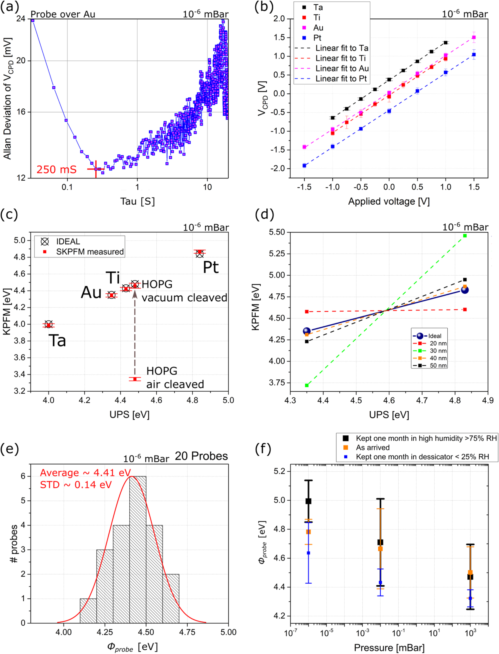
In the spirit of completing the characterization of these type of probes, the spatial resolution (both in terms of topography and KPFM) and the VCPD sensitivity were measured. To do so, a sample consisting of graphene fingers was used (i.e. monolayer graphene, see fabrication details in the Methods section). This sample was chosen due to the small topographic features it presents, which minimize the effect of topography in the KPFM signal [45], and the relative big difference in work function from the graphene to the substrate needed for a good quantification of the KPFM spatial resolution [46]. Figure 3(a) shows the topography of an area with graphene fingers, including a cross section of the height across several fingers. By using the 20–80 rule of Edge Spread Function defined in Standards on Lateral Resolution [47], and an zoomed scan of the fingers area with pixel size ∼1.5 nm, the spatial resolution of the probes was estimated to be ∼3 nm. Figure 3(b) showns the VCPD measurements of the same area as in figure 3(a). A profile across the VCPD over several fingers from the zoomed image, shows that the spatial resolution of the KPFM is ∼20 nm for these probes. By measuring the standard deviation of an homogeneous area (dashed square in figure 3(b)), it was possible to estimate the noise of the KPFM measurements in ∼10 mV.

Figure 3. Topography (a), and KPFM (b) images, of the graphene fingers used to measure the spatial resolution. Lines indicate where profiles shown above where taken.
Download figure:
Standard image High-resolution image2.4. Work function of graphite flakes
In this last part of the study the reliability of the calibration protocol is tested in a real scenario. For this purpose, KPFM measurements are acquired over different surfaces that ideally led to the same work function or same trend (the calibration process on itself has already demonstrated that several probes can agree on the work function of the same sample). To that end, graphite flakes were used as a test-bed sample, because while each flake will present different topography, the work function as a function of the flake thickness should provide a trend which all the probes should be able to reproduce. Thus, it is not required to scan exactly the same area with all the probes, it will be possible to see if a particular flake doesn't follow the trend (i.e. meaning that the calibration is not reliable), and it will be possible to compare the calibration of each probe as they all should measure the same trend of the graphite flakes as a function of the flake thickness.
A set of graphite flakes was exfoliated onto pre-paterned metal electrodes on a Si/SiO2 subtrate (see the Methods section for further details), typically leading to one flake contacting one or two electrodes as shown in figure 4(a). Having two electrodes contacting each flake allows performing conductivity tests to guarantee good electrical connection while allowing to obtain the work function using the measurement process based in biasing the sample with a voltage different than ground (see section 2.2).

Figure 4. (a) 3D topographic image of a graphite flake with the work function superimposed. (b) Evolution of the work function as a function of graphite thickness for 3 different probes. Arrows indicate the estimated value at 0 thickness, ∼4.64 eV, and at infinite thickness (i.e. 'bulk'), 4.38 eV.
Download figure:
Standard image High-resolution image
Using the calibration technique described in section 2.2, and at a pressure of ∼10−6 mBar, a set of graphite flakes was measured and the results are presented in figure 4(b). It is possible to see there that the work function of the graphite flakes changes with thickness, and that the the results obtained using three different probes match each other allowing to reconstruct the thickness dependence. Using a exponential fitting (based only on the experimental results), it is possible to see that at very large thickness the work function tends to ∼4.38 eV, which is lower than the the HOPG measured here, but with error bars that are compatible with the 4.48 eV measured for the HOPG. Similarly on the lower side, for thin flakes, the results presented in figure 4(b) tend to 4.64 eV, a little bit higher than monolayer graphene (∼4.55 eV) [40] but with error bars that are compatible. It is important to note that, for graphene, the work function as a function of number of layers tend to increase/decrease depending on the substrate used as well as with the fabrication method used as much as ∼0.25–1.02 eV [48–51] because of the different doping mechanism between sample and substrate and from the fabrication process.
From these measurerements it is clear the value of a good calibration procedure, as it allows comparing results taken at different moments in time, and even with different probes.
3. Conclusions
We have proposed and demonstrated a calibration procedure for KPFM that allows obtaining the probe's work function with more accuracy and with lower uncertainty than methods based on individual grounded reference samples. This is achieved by calibrating the KPFM probe against several reference metallic samples, previously calibrated by UPS, and using a voltage bias applied to the samples to reduce the uncertainty in the sample's work function measured by KPFM.
The main issues concerning KPFM reproducibility and reliability were also covered, paying particular attention at how to optimize several imaging parameters, which are more often than not overlooked in experimental sections of KPFM imaging papers.
Using the proposed calibration method, a set of Pt-coated probes with different coating thicknesses was tested, showing that this calibration method can be used to identify scaling issues, and thus at the calibration stage faulty probes can be identified and discarded. In addition, spatial resolution for topography, ∼3 nm, and KPFM, 20 nm were also measured, along with probe chemical stability. This last one was tested by placing probes in a high humidity environment and demonstrating no change in respect to as-received probes, thus demonstrating the stability of the probes and the calibration method.
Finally, the calibration method was put to test by measuring a set of different graphite flakes using several different probes and demonstrating that all the results follow the same trend, thus demonstrating that the calibration serves its purpose, i.e. allows comparing results taken under different circumstances.
4. Methods
4.1. UPS
Ultraviolet photoelectron spectroscopy (UPS) spectra were acquired with voltage of −17.82 to −17.91 V applied to the sample. The Fermi edge was centered at 0 eV by measuring the offset from a high resolution Fermi edge spectrum on a silver calibration sample. The offset was then used to correct the energy scale of the measured Pt, Ti, Au and Ta. To calculate the workfunction, the difference in energy between the Fermi edge measured on the silver calibration sample and the cut-off energy, x, is given by  where
where  is the energy of the incident photon. The cut-off energy was obtained by fitting a line to the relevant part of each spectrum, determining its gradient and the point at which it crosses the energy-axis. The resulting work functions are summarized in table 1.
Since UPS characterization was performed in ultra-high vacuum (UHV) it would include all irreversibly bound adsorbates (chemisorbed oxygen and physisorbed hydrocarbon) attached to the surface prior to the measurements giving rise to a level of uncertainty from the reversible adsorption of species, such as water, which may form surface dipoles leading to a small change of the work function when transferring the sample from UHV to ambient environmental conditions. As for example it has been estimated [52] that for Au the work function value experiences a decrease of ∼3% as the relative humidity changes from 0 to 40%.
4.2. Metallic thin films
The metallic thin films used as reference samples in this study were prepared in pairs and deposited onto two different substrastes following the procedures described below.
The Au and Pt films used here (∼30 nm thickness) were deposited onto a Si substrate. The well-defined edges where obtained using standard e-beam lithography in combination with lift-off process. In the first lift-off step the Au film was thermally evaporated, and subsequent, in the same substrate, the Pt film was deposited at room temperature by ion beam sputtering.
In a separated process, 30 nm Ta and Ti films were deposited on top of a Si/SiO2 substrate using an OIPT Plasmalab 400 RF magnetron sputterer (Oxford instruments), and then patterned using UV lithography in combination with a standard lift-off process to obtain a well defined edge.
4.3. Graphene fingers
The graphene fingers used here were epitaxially growth from a SiC substrate by stoping the development before a continuous graphene monolayer was developed through the whole substrate (see [53] for further details).
4.4. Graphite flakes
Graphite flakes were obtained by in-situ mechanical exfoliation of a bulk graphite crystal, and further deposited onto a 300 nm Si/SiO2 substrate with optically paterned Au electrodes (∼60 nm thick).
4.5. Uncertainty sources in KPFM
In the KPFM mode used here [29], the total electrostatic voltage in the probe is a combination of the applied DC voltage, plus an AC component of frequency f', minus the work funtion of the probe  Using
Using  and e as the absolute value of the charge of the electron, the electrostatic voltage can be writen as:

As a result of this voltage, an electrostatic force  appears between the probe and the sample system, which can be modelled as a capacitor. Therefore,
  is related to the rate of changes in the capacitor's energy [16] by:

where C is the capacitance of the capacitor formed between the probe and the sample, z is the vertical separation between the probe and the sample, and  is the electrostatic voltage of the surface, wich can also be written in terms of the voltage applied to the surface minus the surface's workfuntion, i.e.
Now, while equation (2) describes a periodic force with components at different frequencies, the term at frequency 

is of great interest because it can be detected using a lock-in amplifier locked at the frequency f', i.e. amplitude modulation (AM-KPFM), or by locking into the resonant peaks apearing at f0 –f' and f0 + f', i.e. frequency modulation (FM-KPFM) or phase modulation (PM-KPFM), and its minimization implies [30, 32]:

Note that in practice, FM-KPFM or PM-KPFM are preferred for two main reasons linked to higher spatial resolution and repeatability [30, 32, 41]: (i) the shift in the resonance peak of the probe is proportional to the gradient of equation (2) and whilst a change in Vsurf or VDC might produce a small change in the absolute value of equation (2), it can lead to a big change in the gradient, thus making it easier for the feedback loop to achieve the condition stated in equation (4); (ii) the higher frequency of the signal being detected implies that the settling time is shorter and thus faster scanning speeds can be used.
Returning to the calculations, using that the voltage applied to the sample is typically set to zero and that  is usually called
  (i.e. contact potential diference), leads to the familiar expresion used in KPFM:

As it can be seen, equation (7) doesn't depend on the amplitude of the oscillating voltage applied,  or the frequency, f'. This is a consecuence of assuming that the capacitive coupling between the probe and the sample doesn't change due to the probe's oscillations. However, if the capacitance does change periodically due to the oscillating probe, and in concordance with [54], then the condition to minimize the force between the probe and the sample stated in equation (4) becomes:

where the total capacitance has been divided in the capacitance of the tip,  that of the cantilever,
  and VAV
is the average voltage perceived by the cantilever. It can be seen that equation (6) reduces to equation (4) if
and VAV
is the average voltage perceived by the cantilever. It can be seen that equation (6) reduces to equation (4) if  If in addition to the capacitance changing a small error, δ, is introduced when nullifying the electrostatic interaction, then equation (6) has an additional term and becomes:

Which ultimatemly, can be written in terms of work functions and  as:
as:

It can be seen that equation (8) explains the dependency seen in figure 1(e) with the VAC , i.e. as VAC increases, the efect of δ decreases, however, it doesn't explain the dependency of the the VCPD on the frequency f'. This is because equation (8) only takes into account first order corrections, a more detailed expansion (which is out of the scope of this research) will show the dependency between VCPD and f', or effects such as induced charges in the sample's surface [55].
Acknowledgments
This project has received funding from the European Union's Horizon 2020 research and innovation programme under grant agreement GrapheneCore2 785219. Also, additional support was provided by the UK government through the Innovate UK program: Analysis 4 innovators. E C, S S, C C and H C also want to thank the UK government's Department for Business, Energy and Industrial Strategy and the Joint Research Project 16NRM01 GRACE: Developing electrical characterization methods for future graphene electronics. All the authors would like to thank Dr. V Panchal for growth of epitaxial graphene, as well as Oleg V Kolosov, A Tzalenchuk and Olga Kazakova for useful discussions.