
Abstract
Single Cu2O nanowires (NWs) were fabricated by the two-step method we reported previously (Wang et al 2014 RSC Advances 4 37542). Band-edge exciton photoluminescence (PL) was observed from individual NWs at room temperature using excitation at 325 nm. The PL signals were assigned to Fabry–Perot (F-P) type standing waves in a right cylindrical dielectric cavity (resonator) for a representative range of different wire lengths and diameters. We found that the mode spacing of F-P resonances varied inversely as the NW length as expected. For the region of NW diameters from 140 to 200 nm, and NW length between 2–5 mm, E-field simulations by COMSOL Multiphysics finite element analysis indicate that the main F-P mode propagating inside the NW is the HE11 mode. When the diameter exceeds 200 nm, there are at least two F-P type modes supported in the NWs. Our results further the understanding of exciton photoluminescence in Cu2O NWs and demonstrates the existence of enhanced mode frequencies based on the geometry of the optical micro-cavity. We further identify potential applications in exciton-driven optoelectronic devices and light emission enhanced by optical micro-cavities.
Export citation and abstract BibTeX RIS

Original content from this work may be used under the terms of the Creative Commons Attribution 3.0 licence. Any further distribution of this work must maintain attribution to the author(s) and the title of the work, journal citation and DOI.
1. Introduction
Semiconductor optical micro- cavities have received considerable attention due to the need to develop new sources of enhanced light emission for the field of photonics [1–3]. Recently, much interest has been focused on light–matter interaction in nanostructures [4] as an example that offers fascinating optical phenomena to be explored. Semiconductor nanostructures have the potential to create varying types of optical micro-cavities having many different geometries and a range of refractive properties that are desirable to produce strong field confinement from photons created by the annihilation of excitons in a crystalline lattice [5, 6]. Importantly, semiconductor nanowires offer numerous advantages such as a matrix for both creating spontaneous and stimulated emission [7–11]. They subsequently act as a medium for guiding and amplifying the light produced for delivery with minimum losses. An increasing number of studies have shown that effective light emission within semiconductor nanowires can derive from photoluminescence produced by a process of continuous generation and annihilation of excitons. Excitons in various semiconductors present an array of different properties, such as large effective Bohr radius, varying binding energy to lattice atoms or impurities, variable lifetimes before recombination, differing degrees of coupling to lattice phonons, etc Among these excitons in the direct-gap semiconductor Cu2O have some of these attractive benefits such as large binding energy (150 meV [12]), sizeable Bohr radius, and the long lifetime up to 10 μs [12]. Moreover, the existence of multiple Rydberg energies in Cu2O, their susceptibility to size variation by external magnetic fields, and the ability to select excitons having different principal quantum numbers offers the opportunity to produce multiple wavelengths in the photoluminescence series [13]. Currently, Fabry–Perot (F-P) type resonance modes in Cu2O nanowire micro-cavities have not received the attention while that commercially important semi-conductors, such as Si, and Ga(In)As materials, have received. In this work, exciton luminescences arising from the F-P type resonant modes of Cu2O nanowires were detected experimentally using micro-photoluminescence (μ-PL) spectroscopy at room temperature. We carried out Finite-Difference Time Domain (FDTD) simulations on modeled Cu2O nanowires using COMSOL Multiphysics software. These revealed the F-P type resonance exciton eigenmodes that were remarkably similar to the experimentally observed frequencies. We feel this work provides a path toward the development of potential excitonic light sources and helps to advance the understanding of the role that the micro-cavity plays in determining nanowire optics.
2. Results and discussion
Typical Cu2O NWs were fabricated by a previously reported method [24]. Figure 1 shows a top view of the scanning electron microscopy (SEM) images obtained from a typical preparation of NWs. As shown in figure 1(a), the diameters of characteristic NWs fall in the range of 90–285 nm. A magnified SEM image (figure 1(b)) shows an isolated single NW having nearly uniform average diameter of 110 and 153 nm at the upper end and lower end labeled with blue arrows with reasonably straight edges and longitudinal terminations, the single NW has the length of 4.06 μm, as shown in figure S1(d) is available online at stacks.iop.org/JPCO/3/085006/mmedia.
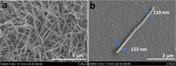
Figure 1. (a) Top view scanning electron microscope (SEM) image of the Cu2O NWs. (b). A magnified SEM image of as-fabricated single Cu2O NW.
Download figure:
Standard image High-resolution imageIn figure 2(a), a schematic experimental geometry for performing PL characterization is present. The PL spectrum of a representative multiple Cu2O NWs on a quartz substrate was obtained at room temperature, as shown in figure 2(b). The PL measurements were obtained using the EDINBURGH Instrument FLS980 Spectrometer. Contributions arising from luminescence of quartz substrate are also shown in figure 2(b). As seen in figure 2(b), the substrate without Cu2O nanowires shows no luminescent peak. The PL spectrum from Cu2O NWs, on the other hand, exhibits a maximum emission peak at 525 nm (i.e. 2.36 eV) as well as multiple ripples comprising subsidiary peak intensities out to beyond 600 nm. We note that this series of weaker emission peaks on the low-energy side of the maximum emission line falls within an energy range from 2.32 to 2.14 eV. It is generally accepted that the band gap energy of bulk Cu2O lies in a range of 2.1–2.2 eV (590–563 nm) depending on surface bonds and impurities [14, 15]. Thus, the series of multiple emission lines on the low-energy side of the maximum emission peak most likely arises from different resonance cavity modes of the NWs [16]. Additionally, there is a weak emission peak at the wavelength of ~405 nm (3.06 eV). This result is consistent with a previous report [17] that attributes the peak to a high energy exciton process in Cu2O.
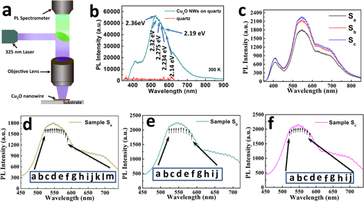
Figure 2. (a) A schematic experimental geometry for performing PL characterization (b) PL spectra with and without Cu2O NWs on quartz under the excitation wavelength with 325 nm at room temperature. (c) PL spectra of three different Cu2O NWs. (d) PL spectrum of the sample Sa. (e) PL spectrum of the sample Sb. (f) PL spectrum of the sample Sc.
Download figure:
Standard image High-resolution imageIn order to test the hypotheses that the series of PL emission lines arise from exciton resonant modes, we examined a representative sample of different NWs to determine the effects of different lengths and diameters on the PL peak distributions. The energy of the excitation from the He-Cd laser operating at 325 nm (3.82 eV) was generally much greater than the exciton resonances we observed (2.17–2.30 eV at room temperature). Figure 2(c) summarizes the micro-PL spectra obtained from single Cu2O NWs using different samples (Sa, Sb, and Sc) having measurably dissimilar diameters and lengths. The corresponding optical images of the three samples are shown in figures S1(a)–(c) of the supporting information (SI). As seen in figure 2(c), all samples exhibit emission peaks in the range between 590–528 nm (2.1–2.35 eV). We attribute their presence to various exciton resonant modes in the different NW cavities. PL intensities of the sample Sc are slightly greater than that of Sb, and the intensity of the sample Sa is the lowest of all these samples. To determine the subsidiary peaks in these PL spectra, we focus on the specific peaks from each sample and label them with tags from a–m in figures 2(d)–(f). Every label points to a peak which likely represents one of distinct resonant modes in the NWs [8]. As shown in figure 2(d), the emission peaks of the sample Sa show a peak spacing between neighboring modes of 21.7 meV. The mode spacing can be calculated according to the following equation: Δλ = λ2/2 L[n–λ(dn/dλ)] [18], where n is the refractive index at the wavelength λ, and L is the measured length of the NW. Here n is assumed to be 2.7, and dn/dλ is about −0.52 μm−1 [19]. We derive a mode spacing of 18.1 nm at the peak resonance of 2.26 eV (i.e. ∼549 nm) for a cavity of measured length L = 3.6 μm. The mode spacing gradually increases to 20.6 nm at 2.10 eV (i.e. 590 nm). As shown in figures 2(e) and (f), the samples Sb and Sc exhibit similar features to Sa at the region of the exciton peak. The exciton PL at the peak at 549 nm, obtained from sample Sb, consists of a series of identical ripples, labeled from a to j in figure 2(e). Their mode spacing is approximately 7.42 nm at the PL peak. Compared with the mode spacing of the sample Sa, the sample Sb presents the smaller mode spacing at the same PL wavelength (∼550 nm). In figure 2(f), the exciton emission peaks from the sample Sc at the 546 nm peak consists of ten identical lines labeled a to j. The measured mode spacing is about 11.35 nm at the peak. The mode spacing, calculated to be 9.7 nm for a measured cavity length L = 4.8 μm, is nearly consistent with the experimental spacing for sample Sc.
In general, the average mode spacing for experimental lines was found to scale inversely with the resonator cavity lengths [19, 20]. Based on optical images of the three samples (shown in figure S1, supplementary information) and the N.A. of the lens (N.A. = 0.66), the optical resolution of the lens is obtained by the equation of d = 0.61*λ/N.A., the value of d is about 0.3 μm. Thus, the resonator lengths could be estimated to be 3.6 ± 0.6, 5.8 ± 0.6 and 4.8 ± 0.6 μm for Sa, Sb, and Sc, respectively. We found for all investigated NWs that the experimental mode spacing closely tracks a linear relationship to the inverse cavity length, as shown in figure S2, supplementary information. This mode spacing was found to be independent of NW diameter (as characterized by the SEM images) over the range between 90 and 285 nm. The mode spacing of the interference peaks is inversely proportional to nanowire length, demonstrating that the nanowire functions as an optical Fabry-Perot (F-P) resonator along its length [21]. Hence, we attribute the multiple subsidiary peaks in the PL spectra to a series of standing-wave Fabry–Perot (FP) resonant modes. For the PL spectra modulated by FP-type resonances, mode energy splitting of the FP modes can be calculated by ΔE = hc/2nL [15], where n is energy dependent refractive index, and L is the cavity length of the sample. For the sample Sa, the calculated mode energy spacing ΔE is determined to be 13.05 meV, a value somewhat smaller than the experimental result above (21.7 meV). Meanwhile, the energy spacing ΔE of Sb is 5.37 meV, and that of the sample Sc is 8.305 meV, confirming that the energy spacing scales with the inverse length of the NWs.
To understand the mechanism by which F-P modes alter the transmission of light down a cylindrical fiber we performed Finite Difference Time Domain (FDTD) simulations of the photon field intensity in Cu2O NWs possessing a step index change to air, as described in the Methods section. For schematic purposes we assumed a generic right circularly symmetric and cylindrical NW having length L, a diameter d, and ask which modes propagate as a function of wavelength (figure 3(a)). In figure 3(b), we calculate the two-dimensional projections of the cross-sectional electric-field distributions along the axial direction for a NW of specific length L = 3 μm, diameter d = 160 nm, and an emission wavelengths λ = 549 nm. These values are similar to the parameters that describe sample Sa. Figure 3(b) shows that the calculated electric-field mode pattern exhibits a periodic enhancement of the electric-field intensity with a fixed axial spacing. In this figure, the deeper the red color that appears, the more intense is the electric field. Figures 3(c)–(e) shows the radial electric-field profiles for the Ex, Ey, Ez components when the effective mode index (neff) of the NW is set constant at 1.6236. Cross-sectional plots of the normalized electric field (Norm.E) are shown in figures 3(f) and (g) for two different effective mode indices. In this case we attribute each distribution to the same HE11a,b mode and consider changes in field distributions produced only by altering the effective FP mode indices [20, 22]. The reasons to consider this possibility are as follows: first, the fundamental HE11 mode is the better confined mode for sustaining a standing wave pattern along the entire wire length compared with the higher order modes; second, the FP resonant modes can be seen to provide the greater confinement of the field distributions within the NWs and maintain internal polarization as shown in figures 3(f) and (g). As both experimental and simulated measurements appear to give similar results for the NW of sample Sa, we conclude that FP resonant cavity modes (standing waves) exist in this sample.

Figure 3. (a) Schematic model of Cu2O NW A for simulation using COMSOL Multiphysics. (b) The simulated two-dimensional electric-field mode distribution  of the NW sample in figure 2(c) for the HE11 confined mode in a 160 nm wide and 3 μm long nanowire at λ = 549 nm. (c)–(e) Electric field intensity profiles for the Ex, Ey, and Ez components of the fundamental HE11 mode in the microcavity of NW A, respectively. (f)–(g) The cross-sectional plots of the normalized electric field in nanowires of NW A with effective mode indices neff 1.6236 and 1.6917, respectively.
Download figure:
Standard image High-resolution imageWe also modeled the cross-sectional electric-fields for the Ex, Ey, Ez components for a PL wavelength of 549 nm, with NW length and diameter equal to those found for samples Sb and Sc. In figure 4 we show the transverse fields for a NW of length L = 5 μm, and diameter d = 200 nm (sample Sb). Similarly, in figure 5 we show the same transverse fields for a NW of length L = 3 μm, and diameter d = 220 nm (sample Sc). Both results were obtained by solving Maxwell's equations for a right circular cylinder of appropriate dimensions. As seen from the simulations, the electric-field intensity projections along the NW axis exhibits periodical dependence on longitudinal position. When the NW diameter exceeds 200 nm, we find two guided modes are supported: both HE11 and TE01 modes become allowed. The cross-sectional plots of the normalized electric fields for these two radial modes are shown in figures S3 and S4 of the supplementary information for several values of the effective mode index.
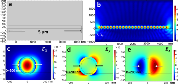
Figure 4. (a) Schematic model of Cu2O NW B for simulation using COMSOL Multiphysics. (b) The simulated two-dimensional electric-field mode distribution  of the NW sample in figure 2(d) for the HE11 confined mode in a 200 nm wide and 5 μm long nanowire at λ = 549 nm. (c)–(e) Electric field intensity profiles for the Ex, Ey, and Ez components of the fundamental HE11 mode in the microcavity of NW B, respectively.
Download figure:
Standard image High-resolution image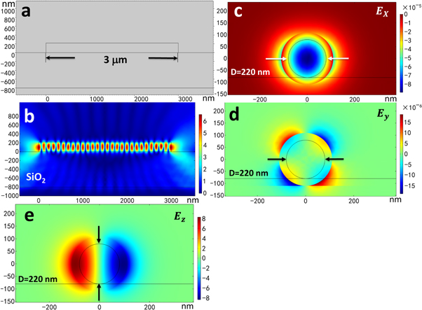
Figure 5. (a) Schematic model of Cu2O NW C for simulation using COMSOL Multiphysics. (b) The simulated two-dimensional electric-field mode distribution  of the NW sample in figure 2(e) for the HE11 confined mode in a 220 nm wide and 3 μm long nanowire at λ = 546 nm. (c)−(e) Electric field intensity profiles for the Ex, Ey, and Ez components of the fundamental HE11 mode in the microcavity of NW C, respectively.
Download figure:
Standard image High-resolution image
To verify the physical origin of the FP modes, we calculated the effective mode indices at 549 nm for the nanowires with various diameters using COMSOL Multiphysics (version 5.3). The results shown in figure S6(a) indicate that effective mode indices drop monotonically as the NW diameter decreases. The effective mode index approaches ∼2.4 for a diameter of ∼320 nm. As the diameter decreases to approximately 140 nm, there are four calculated effective mode indices with neff = 1.0743, 1.18, 1.3635, and 1.4991, which could all support the fundamental HE11 mode. However, the mode indices of 1.0743 and 1.18 do not totally confine the optical field to the nanowire, as shown in figure S5 of supplementary information. As the NW diameter is further decreased, light becomes weakly confined inside the nanowire. More optical field is leaked into the surroundings and the substrate. In figure S6(b), the reflectivity of optical power is calculated using the formula R = (Neff − n0)2/(Neff + n0)2 [19], where n0 is the refractive index of the surroundings. Here, the reflectivity gradually decreases with a decrease in the diameter and then decreases more quickly as the diameter drops below 200 nm. Finally, the reflectivity approaches zero as the diameter approaches ∼143 nm. It exhibits almost zero FP interference peaks as little of the optical field remains inside the NW. Our results for Cu2O nanowires are found to be generally consistent with the properties of Fabry-Pérot micro-cavity modes discovered in single InGaAs/GaAs and CdS nanowires [19, 23].
3. Conclusion
In summary, we report observations of PL eigenmodes of band edge excitons in Cu2O NW micro- cavities. The origin of the eigenmodes is attributed to Fabry–Perot (FP) type resonant modes inside the optical cavity of each NW. The number of modes in the band-edge emission region were observed for three investigational samples that showed a varying number of longitudinal modes (16, 12, and 14) with different splittings. The mode energy spacing depended on the inverse of the NW length. Experimental results and computer modeling of radiation fields demonstrated that FP resonant modes are set up inside the NWs, with modal density favoring the HE11 mode particularly for NW diameters used in this study. In addition, both HE11 and TE01 radial modes (superposed on the FP longitudinal modes) appeared inside the NW as its diameter exceeded 200 nm. The results presented here advance the understanding of exciton PL in the micro-cavity of Cu2O NWs. They show approaches to improving the weak optical processes, such as spontaneous emission, in these devices and suggest potential applications in exciton-related optoelectronic devices where light emission may be enhanced by optical micro-cavities.
Acknowledgments
The authors thank Senior Engineering Yu Wang, A/Prof. Qing Su and Zhenghua Ju for assistance in PL measurements. This work was supported by the National Natural Science Foundation of China (Grants 61204106, 61405077), the Fundamental Research Funds for the Central Universities (Grants lzujbky-2016-119), the Natural Science Foundation of Gansu Province, China (Grants 2016GS08252), and the Science and technology development project of Chengguan District, Lanzhou, China (Grants 2016 CGKJ280).