
Abstract
A facile and economic solution based technique is developed for the deposition of SnO2—Reduced Graphene Oxide (RGO) heterostructure thin films. The single step deposition process leads to uniformly dispersed SnO2 nanocrystallites on well exfoliated RGO sheets as confirmed by x-ray diffraction, Raman spectroscopy and transmission electron microscopy investigations. The response to NO2 gas at room temperature (25 °C) is studied. The interface between n-type SnO2 and p-type RGO flakes forms a hetrostrcuture barrier, which enhances the native sensitivity of pristine RGO towards toxic gases like NO2. The technique allows controlling the density of SnO2 nanoparticles (∼3 nm in size) attached to the RGO flakes and thereby enhancing the response of the heterostructure sensor device. The highest SnO2 loading shows a 14 fold increase in response to 200 ppm of NO2 and a response time as low as 5 s compared to that of ∼200 s for bare RGO films.
Export citation and abstract BibTeX RIS

Original content from this work may be used under the terms of the Creative Commons Attribution 3.0 licence. Any further distribution of this work must maintain attribution to the author(s) and the title of the work, journal citation and DOI.
1. Introduction
Graphene can be regarded as a wonder material as it sports potential applications in various technological fields such as catalysis, photovoltaics, nanoelectronic devices, charge storage, as well as sensors [1–9]. This is particularly due to unique structure, which consists of atom thick layer of hexagonal arrangement of carbon atoms which show remarkable electronic properties like high electrical conductivity, large surface area, a dirac cone and high mechanical- thermal stability.
These aforementioned properties make it suitable for particularly chemical sensor applications as it shows ease of adsorption of gas molecules, which is reflected as change in conduction. Moreover, unlike semiconducting metal oxides based sensors which operate at high temperatures, this adsorption is energetically favored at temperatures as low as room temperature (300 K) [8]. Thus, it shows tremendous potential for low power consumption chemical sensor devices, as it does not require a power-consuming heater in the device architecture. Nonetheless, the adsorbed molecules on graphene layer have high desorption energies at room temperature and hence the sensor signal recoveries are fairly slower for practical applications [9]. Hence, there have been a large number of reports on enhancing the sensor response (i.e. change in conductance) as well as the response and recovery times through functionalization. Functionalizing RGO sheets with either metal oxide (MO) or noble metal nanoparticles, has been found to be a potential approach to improve the properties RGO based chemical sensors. However, the reported synthesis or fabrication of such heterostructures is often a multi-step process, which involves first synthesizing graphite oxide, followed by its reduction and subsequently decorating it with desired nanoparticles. Finally this decorated RGO flakes are deposited either by drop casting, spin coating or similar methods [7, 10–13]. Besides, these techniques often include use of hazardous organic or inorganic chemicals such as benzyl alcohol, hydrazine, NaHBO4 etc.
Here, we report simple, inexpensive single step method for depositing SnO2 nanoparticles decorated RGO sheets thin film, which exhibits high sensitivities for NO2 gas at room temperature (25 °C). The method employed is a combination of solution combustion synthesis and ultrasonic spray pyrolysis and is called Ultrasonic Spray Pyrolysis of Aqueous Combustion Mixture (UNSPACM) [14–17]. The method takes advantage of the exothermicity of solution combustion reaction to obtain nanocrystalline oxide film[14, 15]. Here, the method for deposition of metal oxide thin films is extended for RGO-MO heterostructure thin films, in order to exploit exothermicity for better exfoliation of GO and deposition of MO-RGO nanocomposite films, which have potential technological applications.
2. Materials and methods
Figure 1 shows schematic diagram of the deposition process. Graphite Oxide (GO) was made by Hummer's method[18]. GO was dispersed in water and sonicated for 10 min. Tin oxalate (Aldrich, USA) was carefully dissolved in conc. HNO3 to make tin nitrate. Further, a stoichiometric mixture of tin nitrate and urea was made in aqueous medium. Both the solutions were mixed; such that the final solution contains uniform dispersion of 1 mg ml−1 of GO in water and the concentration of the combustion mixture (CM) are maintained at 0.5, 1.0 and 5.0 mM. The resulting aqueous solutions were used as precursor solution in thin film deposition set up. The films deposited using 0.5, 1.0 and 5.0 mM CM solutions were coded as TOGr0.5, TOGr1.0 and TOGr5.0 respectively. For comparison films were also deposited using only 1 mg ml−1 GO aqueous suspension. The details of experimental set up of UNSPACM method can be found elsewhere [14, 17]. The thin films were deposited at 600 °C with a carrier gas (N2) flow rate of 1000 SCCM. The as deposited films were used for characterizations and gas sensing without further heat treatments.
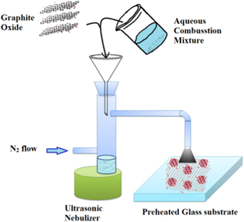
Figure 1. Schematic diagram of film deposition process.
Download figure:
Standard image High-resolution imageX-ray diffraction (XRD) patterns were recorded on a PANanalytical X'Pert PRO using CuKα (1.5418 A°) radiation with a step size of 0.013° in the range of 5–90°. Raman spectra were obtained on Jobin-yvon LabRam HR raman system with a 530 nm wavelength laser in the range from 3000 cm−1 to 100 cm−1. The high-resolution transmission electron microscopy (HRTEM) images were obtained from a JEOL2100F with an accelerating voltage of 200 kV. The Atomic Force Microscopy (AFM) images were recorded on APE Research AFM A100 instrument in non-contact mode.
3. Results and discussion
The x-ray diffraction patterns of the films and GO are shown in figure 2(a). As expected, GO shows an intense peak at 2θ = 10.8°, due to increased interlayer spacing. Whereas, all the films (RGO film as well as TOGr films) show broad characteristic peaks corresponding to (002) reflection of RGO at 2θ = 23.6° as reported in the JCPDS file no. 04-014-0362, which signifies that the RGO sheets are well exfoliated. In case of RGO-SnO2 films the peaks obtained are indexed to rutile type SnO2 according to JCPDS card no 041-01445. The typical crystallite size of SnO2 particles is calculated to be ∼3.5 nm using Scherrer formula.
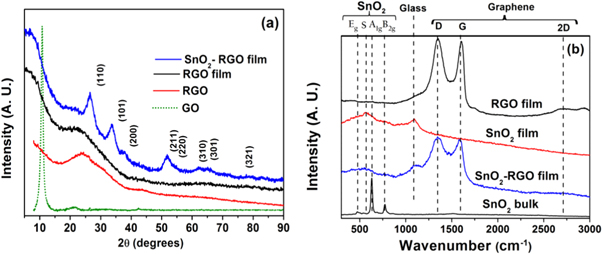
Figure 2. (a) XRD patterns of GO, RGO powder, RGO film and TOGr film. (b) Raman spectra of only RGO film, only SnO2 film, TOGr film along with bulk SnO2 for comparison.
Download figure:
Standard image High-resolution imageThe Raman spectra of the bare and SnO2 decorated RGO heterostructure films are shown in figure 2(b) (along with Raman spectrum of bulk SnO2 and only SnO2 thin films for comparison). The RGO and TOGr films show intense 'D' and 'G' band peaks (∼1340 and 1602 cm−1 respectively). However, both RGO and TOGr films exhibit nearly 1:1 D to G band intensity ratio. Further, in SnO2—RGO thin films the Raman peaks are observed at 769, 627, 473 and 566 cm−1corresponding to B2g, A1g, and Eg vibrational modes of SnO2, here S mode is defect mode, which appears due to smaller crystallite size and hence does not appear in spectrum of bulk SnO2.[15] These results clearly indicate the formation of SnO2 decorated RGO heterostructure films.
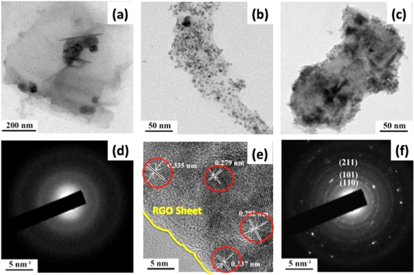
Figure 3. (a) TEM image of RGO film (inset shows SAED pattern of the same). (b) TEM image of TOGr1.0 film (c) TEM image of TOGr5.0 film (d) SAED pattern of bare RGO film, (e) HRTEM image of TOGr1.0 film (d) SAED pattern of TOGr1.0 film indexed for rutile SnO2.
Download figure:
Standard image High-resolution imageTransmission electron microscopy (TEM) images of bare RGO thin films show that the deposition contains well exfoliated RGO sheets (figure 3(a)). Whereas the TEM images of TOGr1.0 (figure 3(b)) and TOGr5.0 (figure 3(c)) clearly exhibit that SnO2 nanocrystals are uniformly distributed over the RGO sheets surface. The High resolution TEM (HRTEM) reveals that the average diameters of the SnO2 particles is ∼3–5 nm (figure 3(e)), which is good agreement with that calculated from XRD. The lattice fringe spacing are found to be 0.335 nm, 0.280 nm, which corresponds to the d spacing of (110), and (211) reflections respectively. The selected area electron diffraction (SAED) pattern (figure 3(f)) consists of three diffraction rings corresponding to the (110), (101), and (211) lattice plane reflections of the rutile SnO2.
The surface topography and film roughness were examined using atomic force microscopy. As it is seen from figure 4, the films show two dimensional (2D) nature of the as deposited films. However, the line profiles show slightly high height profiles as expected for Graphene films. Here, as it can be seen from figure 4, each step size is about 100 nm in height, which means the RGO sheets are highly corrugated. The average roughness calculated is about 100 nm (See supplementary information).

Figure 4. The AFM 3D topography of the TO-RGO film and its line profiles showing 2D nature of the films with steps.
Download figure:
Standard image High-resolution imageHere in this process, the simultaneous reduction and exfoliation of the GO is achieved by rapid heating, which results in thermal decomposition of the oxygen-containing functional groups of GO. Besides, the large amount of interlayer pressure, which results due to the gaseous products, for instance CO2, causes the exfoliation [19–22]. Hence, the thermally exfoliated sheets are topologically rolled up or corrugated, which is also evident from the AFM images.
The gas sensing properties were tested for various concentrations of NO2 gas, in an in-house built gas sensor, which can accommodate four sensors and measure their gas sensing properties simultaneously (See figure 5). This geometry has an advantage in comparing the sensor properties, since all sensors are exposed to same gas environment. The sensitivity (S) was calculated using equation (1).

Where, Ra is Sensor resistance in air and Rg is sensor resistance in presence of test gas. The gas sensing response of the sensors is shown in figure 5. The sensor exhibits good sensitivity at room temperature (25 °C). With increasing SnO2 loading, the sensitivity drastically increases and the response and recovery time significantly reduces (as seen in figures 5(a) and (b)) Further, the sensing response is analyzed using an empirical relation shown in equation (2) [23].

Where, C is concentration of the gas, A is prefactor and exponent β can have values 0.5 or 1 depending on the type of surface reaction and charge on the adsorbing species [23]. The value of β in this case are 0.85, 0.98, 1.12 and 1.24 for RGO, TOGr0.5, TOGr1.0 and TOGR5.0 films respectively, which are close to 1. This signifies similar nature of surface reaction and charge on the adsorbing species for the studied samples. Further the theoretical detection limit is deduced from figure 6(b) and it is found to be as low as 1 ppm for maximum SnO2 loading studied.
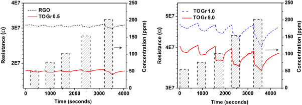
Figure 5. The typical gas sensing response curves of RGO as well as TOGr films.
Download figure:
Standard image High-resolution image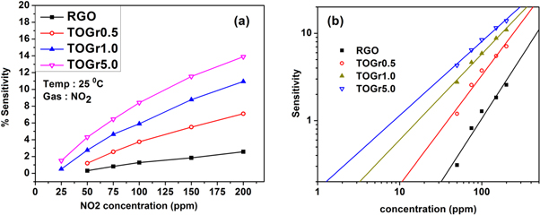
Figure 6. (a) Variation of sensitivity for various NO2 gas concentrations. (b) Log-log plot of sensitivity versus gas concentration for RGO and TOGr films.
Download figure:
Standard image High-resolution imageAs the resistance of the RGO film decreases upon exposure to an oxidizing gas like NO2, it is evident that the as-synthesized RGO as well as TOGr films exhibit a p-type behavior. When RGO sheets are prepared by reducing GO in ambient atmosphere, it results in several electrons withdrawing oxygen containing residual functional groups such as epoxy, carbonyl or carboxylic groups, (see supporting information for XPS data, Figure S5 is available online at stacks.iop.org/JPCO/3/011001/mmedia) along with surface adsorbed oxygen species. This leads to formation of holes in conduction band of RGO, and favours dominant p-type conductivity as compared to ambipolar nature of defect free RGO or RGO obtained from reducing GO in vacuum [10, 24–28].
As shown in figure 7, the interface between RGO and SnO2 nanocrystals results in formation of a heterojunction barrier at the interface of p-type RGO and n-type SnO2 nanocrystals. Since, SnO2 itself is a good gas sensing material, its conductivity changes when target gas molecules get adsorbed on preadsorbed oxygen species present on the oxide surface [29–31]. When an oxidizing gas like NO2 gets adsorbed on SnO2 surface, it traps few conduction electrons and decreases its carrier concentration and thus the conductivity. As SnO2 nanocrystals suffers from loss of electron due to NO2 adsorption, it leads to narrowing of the heterojunction depletion regions, through charge transport across the barrier [10]. This phenomenon leads to electron transfer from RGO to SnO2, resulting in enhancement in carrier concentration (i.e. hole concentatrion) in RGO, thereby increasing its conductivity [10, 32]. Further, upon removing NO2 gas, this charges are restored upon interaction with fresh oxygen surface states with SnO2 nanocrystals. Thus, decorating RGO with SnO2 drastically increases the sensitivity towards NO2 gas. Nevertheless, increasing SnO2 loading on RGO sheets further enhances the sensitivity, as more number of such junctions are formed. The further studies are undertaken to increase sensitivity and other parameters, by estimating maximum SnO2 loading beyond which the current percolates through interconnecting SnO2 particles and kills the RGO contribution.

Figure 7. Electronic band diagram of graphene and tin oxide (a) under flat band condition and (b) upon heterostructure formation.
Download figure:
Standard image High-resolution image
Thus, the main mechanism behind the sensing of this present study is the heterostructure barrier which is formed between p-type RGO and n-type SnO2 nanocrystals. Although, the bare RGO also shows response to the gas at room temperature, it is very weak and slower. The addition of heterostructure junctions not only improves the sensitivity, but also improves the response as well as recovery times. Moreover, since the films consists of 2D sheets of RGO which are decorated with the SnO2 nanocrystals, the films are itself having a higher surface to volume ratio. This is a more efficient design rather than 3D porous materials, where there are parallel networks of grains in all the 3 dimensions. Here, the 2D sheets act as a gas dependent switches and hence have much faster response times.
4. Conclusion
The SnO2 - RGO heterostructure thin films are successfully deposited on glass substrate using aqueous combustion mixture solution and graphite oxide as starting precursors. The films are uniform over large area and show uniformly dispersed SnO2 nanocrystals on RGO sheet, which are well exfoliated. The films show partial reduction of graphite oxide, which is important attribute for gas sensing application. The films exhibit good sensitivity for NO2 gas at room temperature (25 °C), nonetheless it is enhanced on functionalization with SnO2 nanocrystallites. The sensitivity further increases with increasing SnO2 loading and with maximum SnO2 loading studied it can be used to detect upto 1 ppm of NO2 gas with significant sensitivity.
Acknowledgments
The authors thank the Electron Microscopy and XPS facility of chemical sciences division, and Center for nanoscience and engineering (CeNSE) for Raman facility IISc. The authors also thank Mr Amit Vernekar for help and suggestion during graphite oxide synthesis.