
Abstract
Graphene-based thermal rectification was investigated by measuring the thermal transport properties of asymmetric suspended graphene nanomesh devices. A sub-10 nm periodic nanopore phononic crystal structure was successfully patterned on the half area of the suspended graphene ribbon by helium ion beam milling technology. The 'differential thermal leakage' method was developed for thermal transport measurement without disturbance from the leakage of electron current through the suspended graphene bridge. A thermal rectification ratio of up to 60% was observed in a typical device with a nanopore pitch of 20 nm. By increasing the nanopore pitch in a particular range, the thermal rectification ratio showed an increment. However, this ratio was degraded by increasing the environmental temperature. This experiment suggests a promising way to develop a high-performance thermal rectifier by using a phononic crystal to introduce asymmetry on homogeneous material.
Export citation and abstract BibTeX RIS

Original content from this work may be used under the terms of the Creative Commons Attribution 4.0 license. Any further distribution of this work must maintain attribution to the author(s) and the title of the work, journal citation and DOI.
1. Introduction
The energy crisis is one of the biggest current obstacles to the rapid development of human societies. With the explosive development of modern very large-scale integration technology, the issue of cooling computer cores, especially for huge server centres such as Google and Alibaba, results in a huge additional cost. Thermal management becomes more important for today's 'more-than-Moore' era [1]. In this background, the ability to control heat transport in the way that we can control electrical current is one of the desired goals for thermal engineering and energy harvest. This has boosted research into the mechanism of nanoscale heat transport [2–5]. Before a stand-alone thermal information processing system and thermal storage system can be realized [6–8], a high-efficiency basic unit called a thermal rectifier or diode [9–13] that behaves in analogy to an electrical diode needs to be developed. Thermal rectifiers were demonstrated by Starr [14], who showed that the heat flux in the preferred direction is larger than that in the opposite direction. The mechanism in most conventional bulk material devices is based on the different temperature (T) dependence of thermal conductivity (κ) in two different materials which compose the thermal rectifier [11], the so-called conventional opposite κ–T model. This works when each part is large enough for its thermal conductivity to be measured directly. After investigation for almost 100 years, the focus of research is shifting from bulk materials to nanomaterials. However, when a device is shrunk to the nanoscale, it is quite difficult to measure the thermal conductivities for each part of a thermal rectifier. Even with an advanced optical pump measurement system [15–20], the laser spot is of microsize and incapable of working with devices a few 100 nm in size. Besides, thermal conductivity is a macrophysical quantity, and it blankets the basic electron and phonon transport mechanisms in the devices. With the recent development of experimental tools such as focused ion beams [21–26] and advanced simulation methods [27–34] in nanotechnology, researchers have achieved a greatly improved understanding of nanoscale thermal rectifiers beyond their thermal conductivity differences, such as different mass loadings [10, 35], overlap of phonon spectra [36, 37] and the phonon edge scattering effect [38–41]. The discovery of graphene [42–44] has provided an ideal simplified platform to investigate phonon transport on single-layer atoms, and also boosts the utilization of ab initio calculations and molecular dynamics simulation in graphene phonon engineering [45–52]. It has been reported that thermal rectification can be achieved in asymmetric mass distribution systems in which the heat flux tends to go from the heavy mass part to the light mass part [10]. However, another theoretical study [52] shows that by introducing periodic nanopores on half of a graphene nanoribbon, the heat flux is larger from the nanopore region to the pristine graphene region than in the opposite direction, meaning that the heat flux prefers to go from the light mass part to the heavy part. An existing experiment also shows that the phenomenon of thermal rectification can be observed in modified suspended graphene devices by introducing randomly distributed pores of diameter 100–400 nm, and the heat flux is also larger from the pore side (light mass part) than from the non-pore side (heavy mass part) [21]. Therefore, the mechanism of thermal rectification at the nanoscale has not yet been clearly identified. As most of the simulation models with ab initio calculations or molecular dynamics are difficult to extend to more than 100 nm due to the huge amount of computation [45, 47, 48, 51], there remains a big gap between the theory developed from simulations and the results observed from experiments. Therefore there is a much research interest in fabricating suspended graphene devices with a large area of well-controlled periodic nanopores and measuring the thermal transport properties experimentally. Moreover, most of the demonstrated results have a low rectification ratio of around 10%–20% [10, 21, 53]. A high-efficiency thermal rectifier is demanded.
These previous works indicate that introducing asymmetry to the heat transport channel is one of the key points for developing a thermal rectifier, as it induces different influences on phonon transport in different directions. Therefore the application of phononic crystals has been suggested for phonon engineering as a way of controlling phonon transmission with an artificial structure [3, 54–58]. This method has been successfully utilized in silicon-based thermal devices to realize heat guiding and focusing at the nanoscale [18, 19]. Despite this, graphene is also regarded as a promising candidate for application with phononic crystals due to its high Young's modulus, high conductivity and high surface to volume ratio [5, 20]. Therefore, it may be possible to introduce asymmetry by forming a phononic crystal structure in a homogeneous graphene channel; this has not yet been realized experimentally for thermal rectifier applications. In this paper, we report for the first time the observation of thermal rectification on asymmetric suspended graphene nanomesh (GNM) devices with a minimum artificial dimension below 10 nm. A GNM is an artificial phononic crystal structure built on graphene with periodic nanopores. It provides a systematic way to investigate the mechanism of thermal rectification at the nanoscale by changing the pitch or diameter of the nanopores. Furthermore, it leads the possibility of improving thermal rectification performance. Using the helium ion beam milling (HIBM) technique [22, 24], sub-10 nm diameter nanopores were periodically patterned on the right half area of a suspended graphene ribbon (GR) to form the GNM structure shown in figure 1. To characterize the thermal transport properties in two directions, from the GR part to the GNM part and from the GNM part to the GR part, a 'differential thermal leakage' (DTL) method was developed for high-accuracy thermal measurement. The temperature dependence and nanopore pitch dependence of the thermal rectification ratio were also identified. This practical experiment offers a preliminary guideline for realizing a high-efficiency thermal rectifier based on GNM.

Figure 1. Schematic illustration of the asymmetric thermal properties on the half-meshed suspended graphene.
Download figure:
Standard image High-resolution image2. Device fabrication
The device was fabricated using advanced graphene nanoelectromechanical systems (NEMS) technology and HIBM technology [22, 24]. The device structure as determined by helium ion beam microscopy imaging is shown in figure 2(a). In the middle is a 500 nm long, 1.2 µm wide suspended GR. On each side of the GR a gold nanowire is connected, the resistance of which can be measured precisely with a four-probe measurement setting. The asymmetric GNM devices were fabricated using the method reported in [24]. In short, fabrication was started by transferring chemical vapour deposited (CVD) graphene to a SiO2 (285 nm)/Si substrate. The quality of the CVD graphene is shown in the supplementary information (available online at stacks.iop.org/NANOF/5/045002/mmedia). The first electrode layer (80/5 nm Au/Cr) was patterned to achieve good adhesion with the substrate. The graphene underneath was removed by reactive-ion etching (RIE) before deposition of the metal layers. Then the second electrode layer (70/5 nm Au/Cr) was used to make good contact between the first electrode layer and graphene. The GR was formed by electron beam lithography patterning with hydrogen silsesquioxane and plasma etching. After dipping into buffered hydrofluoric acid, the GR was suspended. Then the periodic nanopores were introduced on the right half area of the suspended GR by the HIBM technique, as shown in figure 2(b). In order to avoid collapse during the HIBM process, 100 nm gaps were reserved on the two edges of the suspended GR [24]. By fixing the dwell time of the beam during the HIBM process, the diameters of all the nanopores were kept at the same size of about 6 nm [24], as shown in figure 2(c). The pitch of the GNM is defined as the length from nanopore centre to centre. Two GR-GNM devices were successfully fabricated with pitches of 20 nm and 30 nm, respectively.
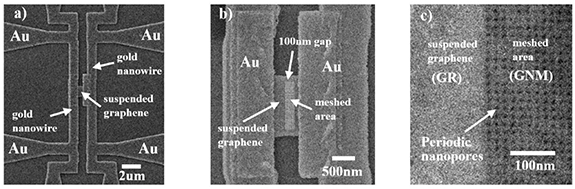
Figure 2. (a) The device structure under a helium ion microscope. (b) The suspended graphene from the helium ion microscope image before HIBM; the dotted matrix is the meshed area. (c) Periodic nanopores on the suspended graphene after HIBM.
Download figure:
Standard image High-resolution image3. DTL method
The performance of a thermal rectifier is usually evaluated from the thermal rectification ratio (ηTR), which is defined as

where  is the environmental temperature,
  is the larger heat flux in one direction and
  is the smaller heat flux in the opposite direction. In these particular devices, the two gold nanowires located at two sides of the suspended graphene bridge (figure 2(a)) can act as heater and heat sink separately. They can form the temperature gradient and create a heat flux through the suspended graphene bridge. In order to check for breakdown of the bridge during the measurement, the gold nanowires and the graphene bridge were designed to be electrically connected. In this case, the general 'H-type' method [59], in which the two gold nanowires work as heater and sensor simultaneously, does not work perfectly. This is because in this experiment the bridge is not an insulating material; also it cannot form a perfect Huygens bridge due to variation in the the microfabrication. Therefore, there would be an electrical current flowing through the graphene bridge to affect the resistance measurement of the sensor part in the general 'H-type' method. This electrical current would also induce an additional electron thermal flux and influence the characterization of phonon transport.
In this paper, the DTL method is developed to avoid the above issue. As shown in figures 3a(2) and b(2), one gold nanowire works as a heater and another works as a heat sink. The electrical current is only applied to the heater, and the heat sink is floating. The suspended graphene bridge works as a thermal bridge to connect the heater to the heat sink. Using figure 3a(2) as an example, a certain amount of heat flux ( ) transports from the heater to the heat sink, and the heater temperature (TR_G) is held at a certain value. By removing the graphene bridge in the same device as shown in figure 3a(1), the heater temperature (TR_NG) will be increased due to the loss of one heat dissipation channel while the same power supply is maintained to the heater. This can be mathematically expressed as

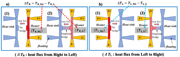
Figure 3. Schematic illustration of the DTL method to show how to measure ΔTR and ΔTL. (a) ΔTR is used to evaluate the heat flux from right to left. (b) ΔTL is used to evaluate the heat flux from left to right. ΔTR and ΔTL are obtained from the temperature differences of the heater between the 'with a bridge' condition and the 'no bridge' condition.
Download figure:
Standard image High-resolution imageAs the device structure is bilaterally symmetrical, the heater and heat sink can swap their roles, and ΔTL can be obtained as shown in figure 3(b)

The relationships between  /
/ and ΔTR/ΔTL are


where  is the specific heat capacity of the heater and
  is the mass of the heater. The heat flux
  from right to left can be evaluated from ΔTR and the heat flux
  from left to right can be evaluated from ΔTL. Then the heat flux from two directions can be compared by measuring ΔTR and ΔTL. Subsequently, ηTR is estimated even without the data for
  and
and  (suppose ΔTR is larger, and ignore the heater mass difference due to the fabrication variation), as

Briefly, the DTL method utilizes the single variable difference method to measure the heat flux through the graphene bridge quantitively by comparing the 'with a bridge' and 'no bridge' conditions. As the heat sink is always floating, there is no electrical current through the graphene bridge. Heat dissipation from the heater (hot gold nanowire) occurs in two main ways (figure 4(b)): one is to the SiO2 substrate and the other is to the graphene bridge (ignoring heat radiation). Based on the fabrication process, the contact area between the heater/heat sink and the graphene channel is sufficiently large that the thermal contact resistance will not limit the thermal transport through the graphene channel. More details are given in the supplementary information.
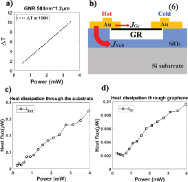
Figure 4. Results of COMSOL simulation with a conventional Joule heating model. (a) Temperature difference ΔT between the 'no bridge' and 'with a bridge' conditions at an environmental temperature of 150 K. (b) Schematic illustration of the main terminals for heat dissipation JSub and JGr. Parts (c) and (d) show the simulation results for JSub and JGr.
Download figure:
Standard image High-resolution imageTo confirm the validity of the DTL method, COMSOL simulation [60] was used to build the same device structure with a suspended GR bridge. The conventional Joule heating model was utilized and there were no nanopores on the suspended GR. In this condition, the heat transport from two directions is the same, so that ΔTR = ΔTL = ΔT. ΔT was calculated to be about 10 K with a 3.5 mW heating power by comparing the 'with a bridge' and 'no bridge' conditions at 150 K (figure 4(a)). These simulation results give the relative expected values for the later measurement results. At the same time, the heat flux through the substrate (JSub) and the graphene bridge (JGr) is shown in figures 4(c) and (d); these are the two main terminals for heat dissipation shown in figure 4(b). The ratio (JSub:JGr) is approximately 33:1 at 150 K with 3.5 mW heating power. Although this is a large ratio, the change in heater temperature (ΔT) caused by JGr is already large enough to be measured by the nanovoltmeter (Keithley 2182A). The COMSOL simulation results confirm that the DTL method is a simple and reliable way to investigate thermal transport in two directions without knowing the thermal conductivities of the materials.
Meanwhile, the simulation results also show the limitations of the DTL method. The JSub:JGr ratio is still too large at 33:1. Although it can survive a qualitative comparison of heat transport between two directions at low temperatures, it will be degraded and lose efficiency at higher temperatures. The thermal conductivity of SiO2 will increase at higher temperatures [61] and the thermal conductivity of graphene will generally decrease at higher temperatures due to the Umklapp process. Therefore, the ratio will be even larger and ΔT will be too small for precise measurement. In this case, decreasing the contact area between the gold nanowire and the SiO2 substrate can help to increase the measurement accuracy. The ideal condition is that the gold nanowires are also fully suspended, but this will greatly increase the difficulty of device fabrication. A partly suspended heater might be a compromise choice in the future. Additionally, decreasing the length of the gold nanowire is a direct way to improve the JSub:JGr ratio. Moreover, replacing gold with platinum may also be a feasible way to increase the sensitivity to temperature change in the future work.
4. Results and discussion
4.1. Electrical current measurement
The measurements were carried out in a cryogenic probe station under high-vacuum conditions (<1 × 10⁻⁶ mbar). Before the thermal measurement, the electrical conductances of the suspended GR-GNM devices from two directions crossing the suspended bridge were checked. A drain voltage (VD = 5 mV) was applied on one gold nanowire while the other one was grounded (figures 5(a) and (b)). The silicon substrate was attached to a grounding chunk. The range of TE was set from 20 K to 300 K. The results in figure 5(c) show that there is no difference in electron transport between the two directions at different TE. In this case, if thermal rectification were to be observed later it would be mainly triggered by different phonon transports.

Figure 5. Schematic illustration of the electrical current measurements. (a) Electrical current from right to left. (b) Electrical current from left to right. (c) Dependence on environmental temperature of the electrical conductance in the two directions for a 20 nm pitch GR-GNM device.
Download figure:
Standard image High-resolution image4.2. Thermal measurement
For the thermal measurements, the TE range was set from 100 K to 300 K, and the resistance–temperature relationship for each gold nanowire was calibrated separately. Two TE points, 150 K and 250 K, were selected to perform the DTL method. The heating power was set from 0.5 mW to 3.5 mW by controlling an electrical current source (Keithley 6220). TL_Gr and TR_Gr in figure 3 were measured first for two GR-GNM devices with 20 nm pitch and 30 nm pitch. Then the graphene bridges were removed by RIE. After reproducing the same measurement, TL_NG and TR_NG in figure 3 were obtained. The computed results for ΔTL and ΔTR with different heating powers at different TE for the two GR-GNM devices are shown in figures 6(a) and (b), respectively. These figures show that the thermal rectification phenomenon can be identified on both the GR-GNM devices, with the heat flux from the GNM side (corresponding to ΔTR) being much larger than that from the opposite side (corresponding to ΔTL). Compared with the simulation result for ΔT in figure 4(a), these measurement results are in a reliable and acceptable range, and the introduction of nanopores definitely decreases the thermal conductivity of the suspended GR.
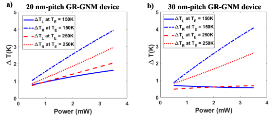
Figure 6. Thermal measurement results using the DTL method at environmental temperatures of 150 K and 250 K for (a) a 20 nm pitch GR-GNM device and (b) a 30 nm pitch GR-GNM device.
Download figure:
Standard image High-resolution image4.3. Factors affecting the thermal rectification ratio
To explore the phenomenon of thermal rectification on GR-GNM devices, the power dependence of ηTR for the two devices in figure 6 is shown in figures 7(a) and (b), respectively. These figures show that ηTR is significantly increased with a larger power supply for both devices at a fixed TE. The larger power supply to the gold nanowire represents a higher temperature difference between the heater and heat sink. This indicates that thermal rectification is sensitive to the temperature difference between the heater and heat sink, which is consistent with previous reports [13, 62]. It is also observed that thermal rectification can be improved by decreasing the environmental temperature. By increasing the power of the heater from 0.5 mW to 3.5 mW at TE = 250 K, the values of ηTR are enhanced by 17.5% for the 20 nm pitch device and 32.7% for the 30 nm pitch device. By decreasing TE from 250 K to 150 K at 3.5 mW, the values of ηTR are improved by 27.9% for the 20 nm pitch device and 12.6% for the 30 nm pitch device. This indicates that TE has an equivalent impact on ηTR as the temperature difference between the heater and heat sink. This kind of TE-induced ηTR degradation is also similar to that found in the previous literature [63, 64]. It is generally considered as being due the larger effect of the Umklapp process at higher temperatures which degrades the asymmetry in the two different parts. To explore the structural dependence of thermal rectification, the power was fixed at 3.5 mW and the pitch dependence of ηTR was extracted at 250 K and 150 K (figure 7(c)). It was found that ηTR is increased with a larger pitch in a certain region. However, it should be noted that ηTR is supposed to be close to 0% with a long enough pitch. The reason for this is that if the pitch is long enough the nanopores can be treated as very low-concentration point defects which have a very limited influence on total phonon transport. Under this condition, the GNM part has almost the same properties as the GR part, and thermal rectification will disappear with an almost symmetric structure. Therefore, more data points are needed in future experiments to clarify the pitch dependence in a larger range. Nevertheless, this implies that ηTR might be not monotonically decreasing or increasing with increasing pitch. In this case, it shows the possibility of improving the thermal rectification ratio as well as increasing the thermal conductivity in the forward direction, because increasing the pitch of the GNM generally will enhance the thermal conductivity. This is good news for the development of high-performance thermal rectifiers. Despite this, by comparing the variation of thermal rectification caused by TE between the two devices in figure 7(c), the ηTR of the 20 nm pitch device is more sensitive to change in TE. To extend application towards a higher TE (room temperature), we propose that a larger pitch in a limited region would help to keep a high thermal rectification performance.
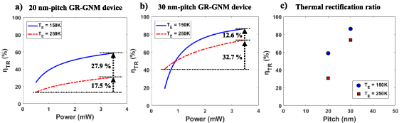
Figure 7. The power dependence of the thermal rectification ratio for (a) 20 nm pitch GR-GNM device and (b) 30 nm pitch GR-GNM device at 150 K and 250 K. (c) The pitch dependence of the thermal rectification ratio at 150 K and 250 K.
Download figure:
Standard image High-resolution image4.4. Potential mechanism
The measurement results are consistent with the phonon results from the Monte Carlo simulation [52] under the frame of the conventional opposite κ–T model. Both sets of results demonstrate that heat flux from the nanopore region to the non-nanopore region is larger than in the opposite direction. However, it is also found that the conventional opposite κ–T model has certain limitations in explaining high-performance thermal rectification in this new kind of device. The details are described in the following.
As a simple explanation, shown in figure 8, the evaluation of the overall thermal conductivities in the two heat flow directions (J+ and J−) is illustrated. The thermal conductivity of the GR part ( ), which is treated as pristine graphene, shows a T−α
decrement in the range 100 K to 300 K due to the Umklapp process in a periodic material [65–67]. For GNM, the edge and defect scattering are thought to dominate the phonon transport, which is almost temperature independent [21, 48]. As a result, the thermal conductivity of the GNM part (
), which is treated as pristine graphene, shows a T−α
decrement in the range 100 K to 300 K due to the Umklapp process in a periodic material [65–67]. For GNM, the edge and defect scattering are thought to dominate the phonon transport, which is almost temperature independent [21, 48]. As a result, the thermal conductivity of the GNM part ( ) is considered to be at a low level and has almost lost temperature dependence.
  and
and  are the base lines (black broken lines) to show the
  –T relationship in figures 8(a) and (c). When the heat flow (J–) is from GR to GNM, the temperature distribution along the suspended channel is shown as the thick purple dotted line in figure 8(b). Based on the 'in series' thermal resistance model [68], as the thermal resistance of the GNM part is larger than that of the GR part, the temperature at the midpoint of the channel (
 ) is higher than (
 −
−  )/2. With the temperature distribution in figure 8(b), the thermal conductivity of the overall suspended channel can be described by the thick green dotted lines in figure 8(a), which includes the thermal conductivity of the GR part (
 ) and that of the GNM part (
 ). Similarly, when the heat flow (J+) is from GNM to GR, (
 ) and (
 ) can also be described, and are shown in figure 8(c) by the green solid lines. As
  is temperature independent,
  is considered to be equal to
  .
.  has a significantly larger value than
  due to the strong temperature dependence of
  . According to Fourier's law and the 'in series' thermal resistance model


Figure 8. Schematic drawing of the conventional opposite κ–T model. (a) Heat flux from GR to GNM called J−. The left thin black broken line is  and the right thin black broken line is
  . The thick green dotted lines overlapping the thin black broken lines represent the temperature dependence of
  , which corresponds to the temperature distribution of the channel (thick purple dotted line) in (b). Similarly, the thick green solid lines in (c) represent the temperature dependence of
  , which corresponds to the temperature distribution of the channel (thick purple solid line) in (b) under the condition of heat flux from GNM to GR, so-called J+.
Download figure:
Standard image High-resolution imagewhere J is the heat current,  is the thermal conductivity, A is the area of the channel cross-section and L is the channel length. As the GNM occupies half the area of the whole channel, the overall thermal conductivity from two directions (
 ) can be written as


Therefore, this indicates that  is larger than
  due to the temperature dependence of
  , and thermal rectification can be identified. ηTR can be obtained as

Subsequently, if the pitch of GNM is increased, the density of nanopores will be decreased and  will be increased. Here we needs to split this into two cases. The first one is that the edge and defect scattering still dominate the phonon transport and
  remains temperature independent. The second one is that the density of nanopores is quite low and
  recovers temperature dependence as
  . The latter loses the asymmetric feature, so it is not the focused point. For the former case, equation (10) can be simplified as

This shows that if  is increased, ηTR will be larger. This numerical trend can be examined quantitatively in COMSOL simulation [60] with the conventional heat transfer model based on Fourier's law.
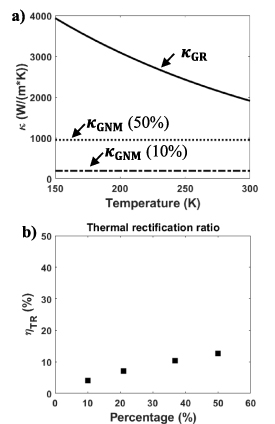
  is estimated according to the CVD graphene data from [21, 66, 69] and the initial value of
  is considered to be 10% of
  at room temperature [70], as shown in figure 9(a). Although figure 9(b) shows a similar trend to that in figure 7(c), by increasing the pitch of GNM, ηTR is found to be limited to below 15% by manipulating
  (10%–50% of
  at room temperature) in this kind of simple and classical heat transfer calculation. It should be emphasized that the
  data in figure 9(a) represent the upper estimated value for a larger area of CVD graphene sheet. When considering the edge effect in a small area of the GR part,
  will be degraded and ηTR will become smaller. Therefore, the ratio in figure 9(b) gives the uppermost value of ηTR. When sticking to the κ–T model there is no way to reach a high value of ηTR. This may be the reason why is quite difficult to achieve high performance with a thermal rectifier based on the conventional opposite κ–T model. Therefore, only using the conventional opposite κ–T model cannot make explicit the mechanism of high-performance thermal rectification in this kind of new device.
Figure 9. (a) The temperature-dependent  and temperature-independent
  data used in the COMSOL simulation. The lower broken line is when
  is equal to 10% of
  at room temperature and the upper dotted line is when it is equal to 50% of κGR. (b) ηTR calculated from COMSOL simulation results. The x-axis shows that
  varies from 10% of
  at room temperature to 50%.
Download figure:
Standard image High-resolution image
It is worth noting that the length of the suspended graphene (500 nm) in this work is shorter than the phonon mean free path (MFP) in suspended graphene (775 nm) [71]. This is a significant difference compared with an early similar experiment [21] in which the devices were a few micrometres long. On a much longer scale, the phase of the phonons will be more randomized due to scattering. Phonon transport is mainly diffusive and incoherent, showing a particle-like behaviour. In this regime, the conventional opposite κ–T model for bulk materials is valid to explain the thermal rectification phenomenon [11]. However, once the length scale is smaller than the phonon MFP, transport will be more ballistic and phonons can travel a certain distance by reserving their phase information. In this case, coherent phonon transport should be considered and the phonons show their wave nature. Once coherent phonon transport is considered in the system, the interface thermal resistance should be emphasized due to coherent phonon scattering at the interface. As coherent phonons have a certain wavelength and MFP length, the scattering would have a strong dependence on the structural dimensions of the incident material and emergence material [67]. This might relate to the observation of high-performance thermal rectification experimentally in this kind of new device for the first time. Therefore, a further coherent phonon transport mechanism needs to be investigated to identify the mechanism of thermal rectification in this kind of device.
5. Conclusion
The phenomenon of thermal rectification has been successfully observed with a high ratio on suspended graphene devices at both 150 K and 250 K by patterning artificial phononic crystal structures on half the area of the channel. Two asymmetric GR-GNM devices were successfully fabricated by combining graphene NEMS technology and HIBM technology to pattern periodic nanopores on large-area suspended graphene. The nanopore diameter was fixed at 6 nm and the pitch of the nanopores was 20 nm and 30 nm, respectively. A DTL method was developed for thermal measurement to evaluate the heat transport properties. The results from the experiment and simulation show that this is a reliable way to investigate thermal rectification in a nanostructure without knowing the thermal conductivities for each part. With the help of this kind of simple method, the heat flux from the GNM part to the GR part was found to be much larger than in the opposite direction in both devices. The measurements also indicate that the thermal rectification ratio can be enhanced by increasing the temperature difference between the heater and heat sink, or by decreasing the environmental temperature. The pitch dependence of the thermal rectification ratio was observed in a limited range. This preliminary experiment indicates a limitation of the conventional opposite κ–T model to explain the mechanism of high-performance thermal rectification in this kind of nanoscale device. The experiment also suggests that nanoscale heat transport might be related to the coherent phonon dominated transport.
Acknowledgments
The authors acknowledge T Iijima and H Ota for use of the HIM at the AIST SCR station for the helium ion irradiation. This work was supported by Grants-in-Aid for Scientific Research Nos. 18H03861 and 19H05520 from the Japan Society for the Promotion of Science (JSPS).
Data availability statement
The data that support the findings of this study are available upon reasonable request from the authors.