
Abstract
In this review, we begin by discussing the need for harnessing renewable energy resources in the context of global energy demands. A summary of first- and second-generation solar cells, their efficiency and grid parity is provided, followed by the need to reduce material and installation costs, and achieve higher efficiencies beyond the Shockley–Queisser limit imposed on single junction cells. We also discuss the specific advantages offered by nanomaterials in enhanced energy harvesting, what design platforms comprise nanostructured photovoltaics, and list the prominent categories of nanomaterials used in the design of third generation solar cells. We review the significant nanostructured photovoltaic platforms that have encouraging power conversion efficiencies, have the potential for long term stability (both structural and functional) and have received attention in the field. In addition to their operational principle, we highlight both their advantages and shortcomings, along with insights into possible improvements. We include alternate routes to improving power conversion efficiency, not by tuning material properties to match the solar spectrum but using additives and/or structural modifications to allow more efficient harvesting of sunlight, either by reducing losses or by altering the spectral properties. The properties of nanomaterials that make them well-suited as active materials in photovoltaic devices (broadband absorption, high quantum yield, etc.) also make them ideal candidates for luminescent solar concentrators (LSCs). These devices also harvest solar energy, but instead of directly allowing charge generation, they act as downconverters for other photovoltaic cells. We review dye, thin film, and quantum dot based LSCs that have garnered a lot of attention in recent years as these devices face a resurgence given the advances in materials science and engineering which have led to novel quantum dots and hybrid semiconductors. The review ends with where the future of nanostructured photovoltaics is headed, what device designs and materials development are needed to achieve efficiencies beyond the Shockley–Queisser limits and fulfil the goal of the 3rd and 4th generation photovoltaics.
Export citation and abstract BibTeX RIS
1. Introduction
Global energy consumption has steadily risen since the 1960s, and the last two decades have seen an increase by roughly 53% [1]. A conservative estimate predicts an additional 35% increase in the next two decades, putting our power needs at an overwhelming ∼30 TW by 2050. While there is a strong possibility that fossil fuels will continue to be a mainstay, an optimistic perspective would be to assume that renewable sources will be tapped more substantively in the coming decades, both for resource conservation and climate preservation purposes. Among the various options available on that front, biomass, hydroelectricity, wind and geothermal resources together can account for almost 14 TWy, but solar energy incident at the Earth's surface is a phenomenal 105 TWy [2]. Needless to say, efficient harnessing of solar energy could not only more than satisfy global energy needs, but do so in a clean, carbon-neutral manner. These obvious advantages have spurred extensive research efforts worldwide, and the influence in the commercial sphere has been notable. The sale of photovoltaic (PV) modules has grown from 1 GW to 100 GW between 2004 and the present [3], reflective of market demand and manufacturing growth. Simultaneously, module prices have dropped by a factor of 5 [4], bringing solar energy closer to achieving grid parity. It is estimated that globally, almost 2% of electrical needs are currently provided by PVs [5], and nearly 90% of the PV market consists of crystalline silicon (Si) solar cells [6].
Si PV belongs to the 1st generation of solar cells and is still the most economically viable PV in use. It has some drawbacks, which have contributed to PVs not having more widespread applications. In the simplest terms, these boil down to the net cost of installing and using solar panels to generate electricity rather than conventional sources. This is measured in terms of grid parity, which currently stands at about 0.1$/kWh [7]. Si PVs are close, but the additional inconvenience of switching over to solar energy would be more attractive to the general populace if this price was closer to $0.03/kWh. There are two routes to achieving this: lowering the manufacturing and installation costs of solar panels or producing panels with higher power conversion efficiency (PCE), or both. And this is where the 1st generation Si panels are problematic. Module and installation prices are unlikely to reduce much more than the present value, and PCE has remained unchanged at a peak value of 25% for the last 15 years [8]. And this limitation is rooted in the inherent material properties. Si has an indirect band gap, which results in low absorptivity, which in turn requires the solar cells be thick to have adequate solar absorption. The cell thickness adds to material costs, to panel weight, and to low PCE as this extra path length gives the photogenerated carriers increasing opportunities to recombine, rather than be extracted as photocurrent. Some of these issues were addressed in the 2nd generation solar cells, which are direct band gap semiconductors and can be fabricated as thin films. Gallium arsenide (GaAs), cadmium telluride (CdTe) and copper indium germanium selenide (CIGS) are representative of this generation, and the most successful is GaAs, with a reported record PCE of 29% [9]. These are commercially even less viable though, given their very high price point. But, these can be fashioned into multijunction cells that are not restrained by the Shockley–Queisser limit and have demonstrated PCEs >40% [10]. The theoretical efficiency of a single junction solar cell is limited to ∼33% by the Shockley–Quiesser [11] formulation, and in practice, single junction cells have not achieved this full potential due to spectral limitations. The inherent inability of a semiconductor to absorb photons with energy lower than its band gap, added to the thermalization of photons with energy higher than it, are both unavoidable loss mechanisms and the only way to overcome them is to fabricate multijunction cells. These make them ideally suited for applications where expense is not a limiting factor, but poundage is, such as space exploration. Returning to terrestrial use, research in the newest generation (3rd) of emergent PVs is motivated by the desire to develop solar cells that allow lost cost synthesis while exhibiting high enough efficiency that would allow them to compete with conventional power generation infrastructure. And a large proportion of these emerging solar cells focus on nanostructured components, both organic and inorganic, which is what this review will emphasize. Before we delve into the wide range of nanostructured PV and their successes and limitations, we take a brief look into the broad context as to why nanostructured materials are considered to have such potential as photovoltaics.
'Small is different' is an oft-repeated but very apt phrase to succinctly describe the unique aspect of nanoscale materials. The reduced spatial dimensions lead to quantization of energy and momentum, and this phenomenon, known as quantum confinement [12], is at the origin of their unique optical, electronic, and magnetic properties that are so different from their bulk counterparts. Additionally, these properties are easily tunable by varying the size of the nanomaterials, or by surface modification [13]. In the specific context of photovoltaic devices, the large absorption coefficient of nanoscale materials is particularly advantageous. less material is needed to harness sunlight, which not only makes the device lightweight and less expensive from the raw materials perspective but allows easier extraction of photogenerated carriers by virtue of a shorter effective path length. And while these will key issues of reducing price while improving efficiency, there are additional advantages offered by nanostructured photovoltaic. The nanomaterials are typically chemically synthesized via low temperature, solution-based methods and therefore, suited for deposition on flexible substrates. The devices thus designed can be applied far more broadly than current rigid solar panels, especially for mobile deployment. This also allows the use of organic materials and others like these that have low mobility. Nanostructured surfaces have lower reflectivity, negating the need for AR coatings and subsequently, the added weight and expense. The definition of what constitutes a nanostructured photovoltaic is quite broad, comprising not only devices that use nanoscale semiconductors as the active material, but also those that incorporate nanoscale optoelectronic components to enhance absorption, induce reflective losses and increase light trapping. In our review, we have exhaustively covered both various, focusing on those platforms that have demonstrated encouraging power conversion efficiencies accompanied by the potential for long term structural and functional stability. While discussing the advantages of each type, we will touch upon the shortcomings, along with any insights into arresting the latter and improving the performance. We include a third category of devices as well, luminescent solar concentrators (LSCs), where the active material is not utilized to directly generate photocarriers. Instead, they act as down converters by absorbing solar radiation and re-emitting it in a spectral region more suited for solar cells attached at the edges. LSCs were initially marketed as a less expensive alternative to silicon solar panels, but with the change in pricing all around, this is no longer a valid motivation. However, LSCs do indeed have unique properties, as they can harvest diffuse radiation in addition to direct sunlight. This is a major advantage over solar cells that require tracking to optimize performance. Further, they are better suited for building-integrated photovoltaic installations than solar panels and will round off our review of nanostructured devices for solar energy harvesting.
We segregate the nanostructured devices in to two broad categories for the purposes of this review. In the first section we will describe and discuss the significant nanostructured PV platforms where the nanomaterials are the active material. These will include dye-sensitized solar cells, quantum dot-sensitized solar cells, quantum dot solar cells, and solar cells that utilize nanowire arrays. In the next section we focus on an alternate route to improving PCE, not by tuning material properties to match the solar spectrum but using nanoscale additives and/or structural modifications to allow more efficient harvesting of sunlight, either by reducing losses or by altering the spectral properties. We will cover plasmonic inclusions that enhance scattering, and absorption, or offer resonant energy transfer and hot carrier injection into the semiconducting photovoltaic, as well as rare earth ions and compounds that act as up or down converters of the solar spectrum to match the absorption band of the active medium to improve performance. We finish off with a description of alternative nanostructured platforms, devices that also harvest solar energy, but instead of directly allowing charge generation, they act as down converters for other PV cells. We will review dye, thin film, and quantum dot based LSCs that have garnered a lot of attention in recent years as these devices face a resurgence given the advances in materials science and engineering which have led to novel QDs and hybrid semiconductors.
2. Nanostructured PV platforms
Nanostructured PVs offer the possibility of increased surface area due to their nanostructured components without increasing the physical size of the device, whereas tailoring of their individual components is significantly easier than conventional Si-based PV as different processes occurring under illumination are decoupled. In this section we highlight the nanostructured PV platforms that have significant and encouraging power conversion efficiencies, and the potential for long term stability. The various technologies that currently satisfy these criteria, and those we will describe and discuss here include dye-sensitized solar cells, quantum dot-sensitized solar cells (QDSSCs) , colloidal quantum dot solar cells, and nanowire-based solar cells. In addition to their operational principle, we will discuss both their advantages and shortcomings, along with insights into possible improvements.
2.1. Dye sensitized solar cells (DSSCs)
DSSCs were first introduced by O'Regan and Grätzel in 1991 [14]. Their work challenged the conventional solid-state photovoltaic cells, by introducing a device that incorporated nanomaterials and separated the processes of light absorption and charge carrier transport. This new device offered the possibility of low-cost photovoltaic devices, which would provide an alternative to power generation from conventional sources.
The first example of DSSC was prepared using a ruthenium complex as sensitizer, deposited on a TiO2 (titanium dioxide) film, and employed a liquid re-dox electrolyte of tetrapropylammonium iodine mixed with iodine. This device achieved a fill factor of 0.76, and in addition to a PCE of 7.9% [14], it also demonstrated an efficiency of 12% under diffuse sunlight, revealing unexpected benefits of these devices compared to conventional silicon based solar cells. Furthermore, under conditions of low light intensity (<5 W m−2), the fill factor remained above 0.7, which is not observed for conventional devices. This was an initial indication of the absence of recombination processes that normally limit device performance in semiconductor devices. The promise shown by this first DSSC encouraged further research into the processes occurring within the device and potential enhancements of the device design to achieve higher PCE .
A typical DSSC is shown in figure 1. The device consists of a glass or plastic substrate, which is coated with a transparent conductive oxide (TCO)—common examples include indium tin oxide (ITO) or fluorine-doped tin oxide (FTO). The substrate is coated with a mesoporous oxide layer, which typically serves as the electron transport layer (ETL) that guides electrons to the anode, and TiO2 has been a particularly popular material for this purpose. Dye is deposited onto the ETL and is employed for light absorption followed by electron injection into the conduction band of the ETL. The dye is then regenerated via electron transfer from the redox electrolyte, typically an iodide/triiodide system. Finally, the triiodide formed is reduced to iodide by capture of electron from the cathode, which usually consists of platinum on TCO glass. These processes are shown in figure 1(b). Therefore, at the end of the process the device has returned to its original state [15]. While extensive research has been done on the materials incorporated in these devices, certain dyes have shown great promise. The most impressive PCE from a single sensitizer so far has been achieved by implementing porphyrin sensitizer (SM315) that has been engineered to improve its light harvesting properties, resulting in a PCE of 13.0% [16].
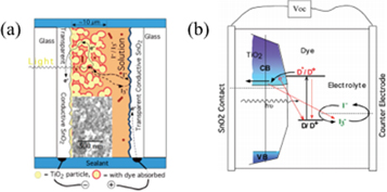
Figure 1. (a) Schematic of a DSSC, and (b) electron transfer processes in a DSSC. Reprinted with permission from [15]. Copyright (2009) American Chemical Society.
Download figure:
Standard image High-resolution image2.1.1. Charge separation, transport, and transfer at dye/ETL interface
Figure 1(b) also shows loss mechanisms that DSSCs are susceptible to. These include direct recombination of the electron and hole pairs in the dye, and recombination of the electrons in the ETL with the oxidized dye or the electrolyte [17, 18]. Hence, optimizing charge injection from the dye to the ETL is crucial for efficient device operation. The dye molecule is responsible for harvesting the incident light energy, resulting in a long-lived excited state, followed by electron injection into the conduction band of the ETL. Two different charge transfer pathways have been identified via femtosecond transient absorption spectroscopy: electron injection from non-relaxed higher-lying excited state, which has been associated with the singlet excited state of the dye, and injection from the fully relaxed excited state, which is associated to the triplet excited state of the dye [18, 19]. These processes compete with back electron transfer from the ETL to the dye, implying that for efficient power conversion, fast electron transfer and slow back electron transfer are needed.
The electron kinetics have been studied extensively in the Ru(dcbpy)2(NCS)2 (RuN3)–TiO2 system, as it is one of the most efficient dye/ETL combinations. Since the lowest excited state of RuN3 is 0.3 eV higher than the conduction band minimum of TiO2, electron injection can occur from the singlet and triplet states of RuN3 [19–22]. By comparing transient absorption signals of the dye deposited on TiO2 and the dye in solution, a shorter time constant was observed for the former case, indicating that a depopulation channel is available. Furthermore, by probing the triplet state absorption, it was concluded that excited state evolution from the singlet to the triplet state is also occurring, with a time constant of approximately 70 fs [19]. The fast component of electron injection from the singlet states has been estimated to occur on a time scale of <100 fs [19, 23–26]. On the other hand, the slow component of electron injection, associated with the transfer from the triplet states of the dye, has been associated with time constants ranging from 1.7 to 100 ps [19, 24–27]. These processes are depicted in figure 2.

Figure 2. Energy level diagram of the RuN3–TiO2 system. Processes: (A) electron injection from the singlet excited state, (B) intersystem crossing, (C) thermalization of triplet state, (D) electron injection from triplet state. Reprinted with permission from [19]. Copyright (2002) American Chemical Society.
Download figure:
Standard image High-resolution imageFigure 2 also shows the energy dependence of the states in the conduction band of TiO2, which has been associated with the variation of the electron injection rate, as it was observed to increase with higher density of states. This has been used to rationalize the presence of a slow component of electron transfer, as the triplet states are close to the energy of the conduction band minimum of TiO2, meaning that there is a reduced density of states available [19, 22, 28]. In addition, while the fast component of electron transfer could occur adiabatically, the slow component could be associated with non-adiabatic processes resulting from the formation of the triplet state [19]. The slow component could also be a consequence of the binding of the dye on the ETL and surface defects [19]. On the other hand, back electron transfer has been observed to happen non-exponentially and is associated with timescales of microseconds to milliseconds, and a negligible picosecond/nanosecond component, therefore reducing competition for the aforementioned electron transfer processes [18, 19]. This difference in timescales justifies the high efficiency of the RuN3–TiO2 system in DSSCs. The slow back electron transfer has been attributed to weak electronic coupling between the oxidized dye and the electron in the ETL, trapping of the electron in the ETL, as well as the inverted Marcus region that slows outer sphere electron transfer [19, 29].
Electron injection studies have been extended to other dyes as well. Work on the Ruthenium bipyridyl sensitizer dye N719 has demonstrated that unlike the RuN3 dye, in which electron injection from the singlet and triplet states is occurring in parallel, electron injection from the triplet state of the N719 dye is the more efficient injection pathway [30]. It was estimated that singlet injection occurs within 1–10 ps, triplet injection occurs within ∼100 ps, whereas intersystem crossing from the singlet to the triplet state occurs within ∼100 fs [19] and decay of the triplet state to ground state requires ∼10 ns. Therefore, Koops et al [30] concluded that electron injection from singlet states occurs only for systems with very favorable interfacial energetics, as is the case in the RuN3–TiO2 system, but for typical devices, due to the presence of the electrolyte which influences the potential, it is unlikely that singlet injection can compete with intersystem crossing. Consequently, electron injection will most likely originate from the triplet state, which results in a ten-fold retardation of injection. This work [30] also investigated the various factors that could influence the electron injection kinetics in a DSSC. While the application of electrical bias or the mere presence of the electrolyte in the device did not affect the injection kinetics, it was found that the composition of the electrolyte had a larger effect. The concentration of tert-butylpyridine (tBP) and lithium cations (Li+) significantly modified kinetics. Incorporation of tBP in the electrolyte is observed to shift the density of states of TiO2 to more negative potentials, whereas Li+ results in less negative potentials. The former changes the conduction band of TiO2 by coordination to the TiO2 surface, or by diminishing the cation concentration on the surface [30–32]. On the other hand, Li+ adsorb or intercalate into the TiO2 layer, eventually modifying the charge and energy levels [28, 30, 33]. However, it was demonstrated that despite the retardation of injection kinetics because of these electrolyte additives, resulting in reduction of the device photocurrent, their presence increases the Fermi level of TiO2 and, consequently, enhances the open circuit voltage of the device, therefore resulting in higher device efficiency. This further establishes the fact that it is not necessary to have the faster injection kinetics for best device performance, but rather a good compromise between driving force that allows competition with dye relaxation and raising the conduction band of TiO2 to reduce recombination losses [30]. Hence, the only requirement is that electron injection from the dye to the ETL happens faster than decay of the excited state.
Although Ruthenium bipyridyl dyes were originally believed to be the best choice for DSSCs, record devices have been prepared with porphyrin sensitizers [16, 34]. Therefore, it is imperative that we discuss the electron injection kinetics of these sensitizers and how they compare with Ruthenium bipyridyl dyes. Ruthenium bipyridyl dyes are characterized by long-lived excited state, good visible absorption, and good photochemical stability [21], as well as a high degree of charge transfer character and mixed singlet/triplet states as discussed previously. On the other hand, other common dyes, including porphyrins, do not show as much mixing of singlet/triplet states and charge transfer, but they also demonstrate long-lived singlet excited states [26, 35–37]. The photophysical characteristics of the two types of dyes are different when in solution; RuN3 exhibits very low emission yield and large red shift of emission, associated with the relaxation of the singlet state to the triplet states, whereas porphyrin dyes (zinc and free base tetracarboxyphenyl porphyrins: ZnTCPP and H2TCPP respectively) show a series of narrow visible absorption bands and small red shift with high emission intensity, characterized by relatively long excited state lifetime [26]. After deposition of all dyes on TiO2, almost indistinguishable, multi-exponential injection kinetics are observed for all, with essentially the same lifetimes and relative amplitudes. This result demonstrates that while for porphyrin dyes electron injection occurs from the singlet state, and for ruthenium bipyridyl dyes charge transfer and relaxation to the triplet state is involved, it does not dominate electron injection kinetics. Furthermore, the recombination kinetics for RuN3 and ZnTCPP are also indistinguishable, whereas H2TCPP demonstrates recombination kinetics that are eight times slower. This result further supports the model that recombination in dyes is mostly controlled by the electron transfer between trap sites in the mesoporous ETL, rather than the electronic structure of the dye [26]. Once the electron is injected into the ETL mesoporous layer, it is transported to the contact, so it can be extracted from the device. Materials such as ZnO and SnO2 have been used in DSSCs, but nanocrystalline porous TiO2 appears to be the best option so far, due to good energy level matching with dyes [38, 39]. The efficient electron transport through the nanocrystalline TiO2 layer is believed to occur by electron hopping from one particle to another [18, 20]. Mesoporous layers are unlike the bulk material as they are characterized by low conductivity, the particles making up the layer are too small to support an electrical field, whereas the mesoporous layer allows for formation of interpenetrating networks that result in a large contact area with the other components of the device [18].
The transport of electrons through the ETL is a complex procedure that has been investigated by multiple research groups. Since the electrons are transported through a trapping and de-trapping mechanism, the traps play a crucial role for both electron transfer and recombination in TiO2 [23, 40, 41]. Traps become important at low illumination intensity, resulting in slow transport and a small diffusion coefficient. At higher light intensity, deep traps are filled, meaning that electron transport is faster and the diffusion coefficient is larger [18, 42]. An additional mechanism regarding the charge transport of TiO2 films has been suggested, indicating that self-doping is occurring under illumination, which results in enhanced conductivity of the originally poorly conductive material [38]. Under illumination, a transient charging process is happening, and when carrier concentration of 1019 cm−3 is reached, the region of the film that is not illuminated undergoes the Mott (insulator-metal) transition, resulting in a significant increase in electrical conductivity [38, 43]. Modification of the TiO2 layer has been attempted by various groups to improve its characteristics, including doping of TiO2 with Zn, Al, Zr, Nb [39, 44, 45], or preparation of 1D nanostructures to enhance electron transport [46].
2.1.2. Liquid electrolytes
For efficient DSSCs, electrolytes must be chosen such that they can transport the charge carriers between anode and cathode successfully, considering the redox potential, regeneration of the dye and the electrolyte. Furthermore, it must ensure good contact with the mesoporous ETL, have minimal leakage and evaporation, as well as long-term stability. In addition, it should not result in dye degradation or desorption, and should not absorb a significant portion of visible light [47–50]. In a DSSC, the electrolyte is acting as a hole-transport medium, and is responsible for regenerating the oxidized dye, with the cycle completed after conversion of the triiodide to iodide at the counter electrode. Therefore, the counter electrode must be chosen to ensure low overpotential and rapid reaction [17, 47, 51]. Platinum (Pt) has been a good candidate for a counter electrode. In liquid electrolytes, ion diffusion occurs via ion hopping or liquid-like diffusion of ionic sub-lattice [47, 52]. However, when there is a high concentration of iodide, polyiodides are formed, resulting in an electron exchange mechanism to be responsible for carrier transportation [47, 53, 54]. In this case, electrons are transported via chemical bond exchanges [53, 55]. Overall, the diffusion process is controlled by the size of the redox species, the solvent viscosity, the redox medium concentration, and the separation between electrodes [47, 56].
In the first example of DSSC, a liquid electrolyte prepared with the iodide/triiodide couple in an organic solvent was used [14]. Liquid electrolytes offer several attractive characteristics: they can be prepared easily, they are highly conductive, they have low viscosity, and can achieve good interfacial contact with the counter electrode [47, 48, 56]. They remain the most common choice for hole transport, and were used in the most efficient DSSCs so far [16, 57]. The liquid electrolyte usually comprises of the solvent, the ionic conductor, and the additives. Good solvents must have melting points below −20 °C, and boiling points above 100 °C to prevent evaporation during cell operation, they must be chemically stable within the operating potential window of the device, have low viscosity to ensure that the redox species has high diffusion coefficient and high conductivity, it should not absorb incident light, it should not react with the sensitizer dye, not dissolve the sealant material, be non-toxic and cheap [47]. While polar organic solvents and ionic liquids are good candidates, a single solvent cannot satisfy all the conditions, therefore solvents are usually mixed. Water was initially used as a solvent in DSSCs, but the oxidation of iodide to iodate, which is not reduced by the counter electrode, prevented long-term operation of the device, whereas many dyes are sensitive to water [17, 47, 56, 58]. Acetonitrile is another good electrolyte as it has low viscosity, good chemical stability and solubility, and was used in the DSSC that achieved record efficiency of 13% [16, 47]. Nevertheless, it suffers from low boiling point and high toxicity, meaning it cannot be implemented in industrial devices. Methoxyacetonitrile and 3-methoxypropionitrile have been used in DSSCs, with the latter demonstrating particularly good stability, retaining 98% of the efficiency after 1000 h of accelerated heat tests under thermal stress [17, 47, 59]. Other common solvents include ethylene carbonate, propylene carbonate, γ-butyrolactone, and N-methyloxazolidinone, which are characterized by high boiling and melting points [47]. A DSSC prepared with γ-butyrolactone solvent has been shown to operate outdoors for almost 2.5 years [60]. It should be noted that basic solvents affect the TiO2 surface, raising its flatband potential, and subsequently not only reducing the driving force for electron injection from the dye to the TiO2, but additionally preventing electron recombination between the TiO2 and the redox species [15, 47, 61]. This results in lower device photocurrent, but higher open circuit voltage.
Ionic liquids have also been incorporated in the electrolytes in DSSCs, as they possess good chemical and thermal stability and high ionic conductivity, while their viscosity can be tailored and they do not evaporate or leak as much [47]. Methyl-hexyl-imidazolium iodide was used in a device that demonstrated impressive stability in 1996 [53]. Later, an electrolyte made with SeCN−/ and without any solvent was implemented, achieving high efficiency at the time (7.5%–8.3%) [62]. The good performance was attributed to the low viscosity, high conductivity, and low light absorption of the ionic liquid, but the stability of the device was not good. Though imidazolium-based ionic liquids are common, other materials that have been used in electrolytes include ionic liquids with sulfonium, guanidinium, ammonium, pyridinium, and phosphonium, but none of these has shown good efficiencies [63–68]. However, implementation of a tetrahydrothiophenium melt demonstrated that ionic liquids can also be used for high efficiency devices [69]. Pure ionic liquids are characterized by high viscosity and low ion mobility, which results in lower diffusion coefficient of the triiodide, in comparison to organic solvents [70]. Hence, in order to improve their performance, ionic liquids are often mixed with organic solvents, which produced devices of high efficiency [71]. Ionic liquids have also been mixed with solid components to improve their conductivity [72]. Mixing with multi-walled carbon nanotubes resulted in significant improvement of device efficiency [73].
The iodide/triiodide redox couple has traditionally been used in DSSCs for dye regeneration, as it has a redox potential that matches that of the dye, thereby ensuring rapid dye regeneration and slow recombination. Furthermore, this redox couple is soluble, conductive, does not absorb as much visible light, has good stability, and can form good interfaces with the mesoporous ETL [47]. One of the issues of DSSC operation is the recombination of charge carriers at the interface between the ETL and the electrolyte, which can be suppressed by incorporation of a metal oxide blocking layer [74]. It can also be suppressed by introducing additives such as 4-tert-butylpyridine and guanidium thiocynate in the electrolyte [21, 47, 75–77]. Similarly, dyes that have hydrophobic chains also appear to prevent recombination by blocking the contact of the two materials [78], whereas other dyes have the reverse effect of increasing the amount of triiodide near the dye [79, 80]. In order to increase the rate at which the dye is regenerated, the concentration of iodide must be tailored depending on whether organic solvent or ionic liquid is used; higher concentration is needed for the latter due to its lower viscosity [81]. Even though the iodide/triiodide redox species has been used for a large number of DSSCs, it suffers from issues of encapsulation due to the high vapor pressure of iodide and corrosion of the sealant by the iodide, while the polyiodides absorb part of the incident light, limiting the photocurrent [47]. In addition, the mismatch between the redox potential of the dye and that of the redox species causes a reduction of the possible open circuit voltage that can be achieved [47, 82]. As a result, alternative complexes were pursued. These include bromide/tribromide [51], interhalogen redox systems [83], disulfide/thiolate [84], and most notably, cobalt complexes [16, 34, 57]. Cobalt complexes have been used in both devices that currently hold the efficiency record [16, 57] and are considered to be the most efficient redox species for DSSCs, with further improvements expected after tuning the redox potentials of the redox couple [47]. Other metal complexes that have been studied include Ni(III)/Ni(IV), Cu(I)/Cu(II), and ferrocene/ferrocenium [85–89].
Electrical additives are often included in the electrolyte to optimize device performance. As mentioned in sections 2.1.1, 4-tert-butylpyridine (tBP) is a common additive, which improves the open circuit voltage, by shifting the conduction band edge of TiO2 to more negative values [47]. Additives with similar effects include various nitrogen-containing compounds, such as pyridine, alkylaminopyridine, alkylpyridine, benzimidazole, pyrzaole, quinolone, among others [47]. Another type of additive, also mentioned in the previous section, are lithium ions (Li+) or guanidinium ions, which adsorb to the surface of TiO2 and assist in electron injection from the dye and reduce electron recombination by attaching to the surface of the TiO2 layer, thereby improving the device photocurrent. Both types of additives are often combined in devices in order to acquire benefits from each one: raising the conduction band of TiO2 and minimizing recombination losses [90–92].
2.1.3. Solid-state hole transport materials (HTMs)
Liquid electrolytes suffer from instability and leakage issues under exposure to air and prolonged storage. Therefore, research focus shifted to developing solid-state HTMs to avoid such problems. The redox electrolytes discussed in section 2.1.2 can transport charge carriers via ion movement and can be essentially considered a hole-transport layer. Thus, they could be replaced by p-type semiconductors, which are also capable of hole-transport via hole hopping through neighboring molecules [47]. A good HTM must have its valence band maximum above the ground state energy level of the dye to allow for efficient hole transfer and should be characterized by good hole mobility [93–95]. Furthermore, it should not absorb visible light, or cause dye degradation. [96, 97] In addition, as sufficient pore filling of the mesoporous ETL is crucial, the HTM should allow for deposition in an amorphous state to ensure good contact between the various layers of the DSSC [98, 99]. Some of the first types of inorganic solid-state HTMs included copper compounds (CuI, CuBr, CuSCN) [100–103]. These materials allow for solution or vacuum deposition, and are characterized by good hole conductivity [97]. CuI was incorporated in a DSSC for the first time in 1995, with low efficiency, which was attributed to the rapid crystallization of CuI that prevented sufficient filling of the mesoporous ETL and hence, caused insufficient electrical contact [95, 100]. After addition of 1-methyl-3-ethylimidazolium thiocyanate (MEISCN), which acts as a growth inhibitor for CuI, improved pore filling was achieved, leading to increased device efficiency of 3.8% [104]. Nevertheless, devices based on CuI HTM decay rapidly, because of the formation of Cu2O and CuO caused by the iodine molecules on the surface of CuI acting as hole trapping sites [47, 105–107]. Introduction of a MgO blocking layer increased device efficiency by preventing hole transfer from TiO2 to CuI [108]. The low efficiency of these devices could also be attributed to the insufficient contact between the dye and the HTM. However, it was observed that dyes with thiocyanate ligands can be strongly bound to CuI films, improving contact and therefore, device efficiency [109]. Further modification of the Cul HTM and the counter electrode with guanidine thiocyanate enhanced device performance, reaching device efficiency of 7.4% [110, 111].
CuSCN was investigated as an alternative to CuI, as it could offer higher stability [47, 101]. However, CuSCN suffers from low hole conductivity which necessitates material engineering to improve its electrical characteristics. Doping with (SCN)2 led to the formation of acceptor levels below the CuSCN band gap, whereas inclusion of Cu(II) sites in CuSCN increased its hole conductivity, with both modifications resulting in improved device performance [112, 113]. Another promising solid-state HTM is cesium tiniodide (CsSnI3), which demonstrates high hole conductivity and hole mobility, and a band gap of 1.3 eV [47]. Since CsSnI3 can be prepared by solution processing, it allows for good pore filling of the mesoporous ETL, whereas its low band gap improves light absorption at longer wavelengths. Its incorporation in a DSSC resulted in device efficiency of 3.72% and doping of CsSnI3 with SnF2 raised the efficiency to 6.81% [47]. Through additional device engineering, CsSnI3-based DSSCs reached efficiency of 10.2% [114]. Further modifications include use of Cs2SnI6 instead of CsSnI3, which is stable in air and moisture, allowing for device fabrication in air [115].
Organic HTMs offer certain benefits over inorganic materials, such as abundancy, low cost, and facile preparation [47, 116]. and can be broadly classified into polymeric and molecular HTMs [116]. Polymeric HTM polypyrrole was first implemented in a DSSC in 1997, but it performed poorly due to absorption of visible light [117–119]. Polyaniline was also introduced as a potential HTM, but only reached device efficiency of 1.15% [120, 121]. Poly(3-hexylthiophene) (P3HT) and poly(3-octylthiophene) (P3OT) have dominated the polymeric HTM research landscape since then. While initial device efficiencies were low due to insufficient pore filling of the mesoporous TiO2, device engineering boosted efficiency to 1.3% and demonstrated good stability after 3-month storage in air [122–125]. Device efficiencies were further enhanced by addition of bis(trifluoromethanesulfonyl)imide (LiTFSI) and tBP to P3HT reaching 2.7% [126, 127], as well as successful infiltration of P3HT into TiO2 nanotubes [128]. Combination of P3HT with [6,6]-phenyl-C61-butyric acid methyl ester (PCBM) further increased device efficiency to 4.11% [129]. One of the most promising polymeric HTMs is poly(3,4-ethylenedioxythiophene) (PEDOT), which is characterized by minimal absorption in the visible part of the spectrum, good hole conductivity, and good stability at room temperature [47]. DSSCs incorporating PEDOT have reached efficiency of 6.8% [130]. Among molecular HTMs, 2,2',7,7'-tetrakis(N,N-di-p-methoxyphenylamine)-9,9'-spirobifluorene (spiro-OMeTAD) is one that has shown remarkable results [47]. It initially resulted in device efficiency of 0.74% due to charge recombination at the spiro-OMeTAD/ETL interface [93], but through doping of the material with FK102 cobalt(III) complex that increased its hole mobility, and combination with Y123 sensitizer, device efficiency of 7.2% was achieved [131]. Even though solid state HTMs show better long-term stability, they still lag in device efficiency in comparison to their liquid-based counterparts, due to electrical contact issues with the rest of the device layers [47].
2.1.4. Progress on the main limitations of DSSCs
While significant improvements have been made in the materials incorporated in DSSCs, there are still issues to be resolved before the efficiency can be enhanced further. Extensive work has been done on understand and addressing each of these.
2.1.4.1. Absorption in the near-infrared spectral region
The first record efficiencies in DSSC research were achieved by implementation of the ruthenium N3, N719, and black N749 dyes. These dyes performed well as sensitizers in the visible part of the spectrum, but failed to absorb well in the near-infrared part of the spectrum, which, as shown in figure 3, is a significant portion of the solar spectrum [17, 132]. Therefore, it is imperative to develop dyes with improved response in the region of the spectrum beyond 900 nm to achieve high power conversion efficiencies. To meet this requirement, various types of sensitizers for DSSCs have been developed. Metal complexes, including ruthenium, have been popular due to their broad absorption spectrum. These sensitizers consist of a metal ion and ancillary ligands with an anchoring group, with the absorption in the visible part of the spectrum associated with a metal to ligand charge transfer [17]. The ligands are tuned to modify the properties of the sensitizer to achieve higher device performance.
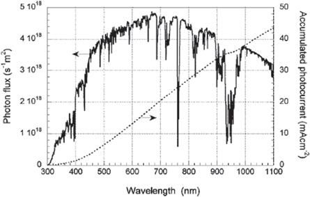
Figure 3. AM 1.5 G spectrum at 1000 W m−2 and accumulated photocurrent. Reprinted with permission from [17]. Copyright (2010) American Chemical Society.
Download figure:
Standard image High-resolution imageRuthenium N3 dye has been commonly used due to its broad absorption in the visible part of the spectrum, leading to efficiencies of 10% [15]. By modifying the ligands to extend the absorption spectrum to the near-infrared region, the N749 'black dye' was designed, which successfully extended IPCE to 920 nm, and resulted in PCE of 10.4% [133, 134]. Other efforts include preparation of a ruthenium dye with a tetradentate ligand, which extended the absorption spectrum to 900 nm, resulting in efficiency of 5.9% [135]. Due to a modification of the HOMO and LUMO levels of the dye, improved spectral response was achieved, resulting in device efficiency of 8.7% [136]. Introduction of thiophene ligands was observed to alter the energy levels of the dye, red-shifting the absorption spectrum [17]. Therefore, this lead to a 10 nm red shift of the absorption, and a device efficiency of 9.5%, when the modified N719 was implemented [137]. Other metal complexes were also investigated in the efforts to achieve improved near-infrared absorption. By replacing the ruthenium ion with osmium, the IPCE spectrum was extended to 1100 nm, while maintaining good device performance [138].
Porphyrins are also of significant interest in the effort to achieve good absorption in the near-infrared part of the spectrum. They demonstrate strong absorption in the Soret band (400–450 nm) and the Q-band (500–700 nm) [139], indicating that they can operate as panchromatic sensitizers, with efforts made to enhance the Q-band. Porphyrin dyes with a donor-π-acceptor structure, with porphyrin as the donor, and cyanoacrylic acid as the acceptor, can be tuned through various thiophene derivatives which act as the π bridge and can be used to enhance the absorption of the dye [17, 140]. Such a dye was used to achieve record device efficiency of 13% with a single sensitizer, as addition of the proquinoidal benzothiadiazole resulted in broadening of the Soret and Q-band absorption, reaching 800 nm [16]. Phthalocyanines are another type of dye that demonstrate high absorption around 700 nm, and are thus candidates for good absorption in the near-infrared part of the spectrum [17]. Nevertheless, these dyes suffer from poor solubility and aggregation on the ETL surface, necessitating the use of a co-adsorber [17]. A Zn-phthalocyanine dye has demonstrated maximal IPCE in the near-infrared region, but the device efficiency was only 0.57% [141].
Extensive work has also been done on this front on organic dyes, as they also possess a donor-π-acceptor structure, which makes tuning of their absorption spectra easy [17]. Vinylene units were introduced into coumarin sensitizers to extend their absorption spectrum, producing dyes characterized by broad red-shifted absorption, due to a shift of the HOMO level to higher energy, and resulting in device efficiency of 6% [17, 142]. Device performance based on coumarin dyes was enhanced by introduction of thiophene units, as vinylene units proved problematic for dye aggregation, achieving efficiency of up to 8.1% [17, 143]. Furthermore, addition of more cyanate groups to the π bridge of the dye resulted in additional extension of the absorption spectrum [144]. Indoline dyes showed a broader absorption spectrum after incorporation of a rhodamine framework, reaching efficiency of 9.5% after optimization of the dye structure and accompanying ETL [145–147]. One of the highest near-infrared IPCE values for organic dyes of donor-π-acceptor structure was achieved using a tetrahydroquinoline dye, through modification to separate the anchoring and acceptor group, resulting in device efficiency of 3.7% [148]. The broadest IPCE spectrum of organic dye-based DSSCs reached 920 nm and was achieved by incorporation of a phenoxazine dye with a thienyl π bridge and a corhodanine acceptor [149]. Other organic dyes that have been engineered for red-shifted absorption include N,N-dialkylaniline dyes which reached 6.8% efficiency [150, 151], squaraine dyes which show good absorption in the near-infrared region [17, 152], and boradiazaindacene dye, which has a near-infrared absorption spectrum (600–800 nm) and produced a device of 1.7% efficiency [153].
Despite the extensive work that has been done on this aspect of DSSCs, an optimum sensitizer that can cover the entire solar spectrum has not been fabricated yet, although mixing of different sensitizers has been implemented in devices with impressive results [18, 57]. It has been estimated that by extending the absorption spectrum to 920 nm, PCE of 19% can be achieved [154].
2.1.4.2. Leakage in DSSCs
While the most efficient devices yet have been fabricated with liquid electrolytes [16, 57], the use of liquid electrolytes faces issues associated with leakage of the solvent and subsequent instability of the photovoltaic performance of the device, inhibiting commercialization of DSSCs [47]. This encouraged research into alternative materials for hole transport and dye regeneration, which resulted in solid-state DSSCs, but despite demonstrating good stability, they suffer from reduced efficiency due to low conductivity and poor pore filling, and therefore poor electrical contact, of the mesoporous ETL [47]. Work was also done to develop quasi-solid electrolytes, such as polymers [155, 156], and gels [157], but, like solid-state HTMs, they are also plagued by reduced transfer rates of the redox species because of the increased material viscosity and poor contact with the electrodes, meaning that device efficiency of devices incorporating quasi-solid electrolytes remains below (8%–9%) that of DSSCs prepared with liquid electrolytes [47, 158]. This issue has not been resolved yet, but advances are constantly being made towards achieving more stable DSSCs.
2.1.4.3. Photo-bleaching in DSSCs
DSSC stability is not only due to leakage and evaporation of the liquid electrolyte, but also limited by degradation of the electrolyte under long-term irradiation by sunlight, and in particular, ultraviolet (UV) light [51]. The ETL, commonly TiO2, absorbs UV light to form excitons, and the photogenerated holes might react with any other component that is not the iodide, leading to a depletion of triiodide in the device, which hinders the proper operation of the device [159–161]. The lack of redox couples in the device has further implications on the dye stability. As the dye is not reduced, it could react with other elements in the device, producing new species are cannot be used for generation of charges [159]. This has been observed to lead to a significant drop in short-circuit current. Nevertheless, this effect is initially negligible in a full device until the concentration of redox species is significantly quenched, and only a reduction of open-circuit voltage is observed that is associated with reduction of redox species in the electrolyte [159]. Efforts to improve the stability of the electrolyte under UV irradiation include incorporation of UV filters [51, 162], as well as electrolyte additives which can enhance its stability, such as MgI2 and CaI2 [162]. MgI2 appears to perform best for this purpose, and the mechanism behind the improvement is still unclear, although it could be the formation of a MgO surface layer which prevents the reactions between the ETL and the electrolyte, or the reduction of the holes in the ETL by the iodide [162]. Nevertheless, this is another key issue that needs to be addressed before DSSCs can reach the stability level suitable for commercial devices.
2.2. Quantum dot-sensitized solar cells
QDSSCs operate much like DSSCs. In these devices, the sensitizer layer now consists of quantum dots (QDs) instead of a dye, on a mesoporous semiconductor which serves as the ETL, such as TiO2 or ZnO [163, 164]. The solar cell is completed by the electrolyte or HTM, and the counter electrode. As outlined in figure 4, when sunlight is incident on the QDSSC, the QDs will absorb light to generate electron–hole pairs. The electrons are then transferred from the conduction band of the QD to the conduction band of the ETL, and the holes are transferred to the electrolyte/HTM, which is typically made of polysulfides. The oxidized electrolyte is then reduced to its original state by electrons re-entering the cell from the external circuit [163, 165]. The open-circuit voltage is determined by the difference between the fermi level of the QD/ETL system and the redox potential of the electrolyte, whereas the produced current is controlled by the sensitizing ability of the QDs and the efficiency of electron separation and extraction [163, 166]. QDSSCs have become an attractive alternative to DSSCs due to ease of fabrication, tunable spectral properties allowing for tandem architectures, improved stability over DSSCs as they can form better junctions with solid state HTMs, and the potential of multiple exciton generation by impact ionization that could increase the theoretical limit in efficiency to 44% [163–165, 167–169]. The current best efficiency recorded for QDSSCs is 11.61% [170], and while significant enhancements have been achieved in the past few years, the record efficiency is still below the record efficiency of DSSCs [165].

Figure 4. (a) QDs on TiO2 nanoparticles, (b) operating principle of a QDSSC [165]. Common QD sensitizers include CdS, CdSe, CdTe, PbS. Reprinted with permission from [165]. Copyright (2009) American Chemical Society.
Download figure:
Standard image High-resolution image2.2.1. Size tunable properties
Implementation of QDs offers a variety of benefits over dyes as sensitizers in a solar cell. Perhaps their biggest benefit is the ability to tune their spectral properties easily by varying the diameter of the QD, due to quantization effects present. By modifying the energy levels of the QDs, light absorption and electron injection can be tailored to match the needs of the solar cell [171, 172], whereas generation of multiple excitons by a single photon and hot electrons offer new possibilities for enhancement of device performance [171, 173].
Good QDSSC operation requires that the conduction band of the QD sensitizer be higher than the conduction band of the ETL for efficient electron transfer between the two, as the offset provides the driving force for charge transfer [163, 171]. While the open circuit voltage of the device is independent of the size of the QDs used in the sensitizer, as demonstrated in figure 5(a), the device photocurrent is directly correlated to the properties of the QDs [171]. It has been observed that smaller QDs result in higher photocurrent due to the higher conduction band as shown in figure 5(b), implying that a larger driving force will be available for electron injection to the ETL [171, 174]. However, decreasing QD size is also associated with more limited response in the visible part of the spectrum as shown in figure 5(c) [171].
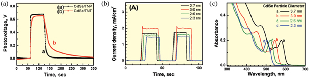
Figure 5. (a) Open-circuit voltage for TiO2 nanoparticles/3 nm CdSe QDs and TiO2 nanotubes/3 nm CdSe QDs, (b) photocurrent of TiO2 nanoparticles/CdSe QDs of various sizes, (c) absorption spectra of CdSe QDs of various sizes. Reprinted with permission from [171]. Copyright (2008) American Chemical Society.
Download figure:
Standard image High-resolution imageThe emission decay of CdSe/TiO2 electrodes was used to estimate electron transfer constants through measurement of the recombination rate constants [170, 171]. Exponential decay models were implemented to extract emission lifetimes, and it was observed that for smaller nanoparticles, shorter electron transfer constants are obtained [171]. Furthermore, there was no apparent difference between the QDs on TiO2 nanoparticles and TiO2 nanotubes, indicating that the morphology of the ETL does not influence the charge injection process. This further supports the evidence that photocurrent is dominated by QD properties. IPCE was also seen to improve with smaller QDs, establishing that since they possess a more energetic excited state, their electron injection rate is higher. The morphology of the ETL becomes important where open-circuit voltage is concerned. As seen in figure 5(a), the photo-voltage of the solar cell decays more slowly after illumination stops for the TiO2 nanotube substrate, which is direct indication that the electrons injected in the TiO2 have a longer lifetime before recombination, hence the tubular structure can be used to minimize losses at grain boundaries [163, 171]. Therefore, both smaller and larger QDs offer different benefits for the solar cell and its operation. Thus, a tandem structure ('rainbow' configuration) has been proposed for QDSSCs, which would leverage benefits from both small and large QDs [163, 171]. A gradient assembly of QDs of various sizes could be used, in which small QDs would absorb light of higher energy, allowing longer wavelengths to be transmitted and eventually be absorbed by larger QDs below them. This would utilize the fast electron injection of small QDs and high absorption of large QDs at the same time [171].
This concept has also encouraged research into alloyed QDs which would combine the beneficial properties of various materials to fabricate QDs that are most suitable for QDSSCs [163, 175]. This has led to the preparation of the champion device with 11.61% certified efficiency, which used 4 nm Zn-Cu-In-Se QDs as sensitizers and combined absorption onset of 1000 nm and fast electron injection rate of 9.1 × 10¹⁰ s−1 [170].
2.2.2. Stability improvement
Another major benefit of QD sensitizers is the potentially higher stability of QDs in oxygen and water, in comparison to molecular dyes [176]. While originally the iodide/triiodide couple was implemented in QDSSCs as well, it was observed to be detrimental to QDs which were unstable in this electrolyte [163, 165]. Instead, the sulfide/polysulfide system was implemented as redox couple, with good results [177]. Nevertheless, this has shown issues with low open-circuit voltage due to the high redox potential of the polysulfide electrode, and various techniques to address this issue have been used, including adjusting the concentration of the redox couple, changing the solvent composition, and incorporating additives [178–181]. However, the inability of the polysulfide electrolyte to scavenge holes from QDs efficiently has been a source of device instability, as the QDs oxidize and subsequently degrade [175]. This has encouraged research into alternative electrode materials, which resulted in improved device fill factor and enhanced stability [165, 175, 182]. Such materials include Cu2S or Au, instead of the typical Pt. Furthermore, QDs with enhanced stability have been engineered to address this issue. Alloyed QDs are observed to demonstrate increased stability in the polysulfide environment in comparison to QDs prepared with the constituent materials [175, 183].
Like DSSCs, QDSSCs also face instability issues due to leakage of the liquid electrolyte [170]. Research efforts to implement quasi-solid and solid-state electrolytes in QDSSCs, such as ionic liquids, gels, hydrogels, spiro-OMeTAD, and P3HT have met with great success [184–188]. QDSSC with a gel electrolyte combined with CdSexTe1−x QDs has demonstrated power efficiency of 9.21% [189], whereas a device with CuS QDs and P3HT has produced PCE of 8.07% [190]. QD-sensitized ETLs appear to form better junctions with solid-state electrolytes as compared to dye-sensitized ETLs, as the thinner layer of sensitizer alleviates the issue of insufficient penetration of the solid-state electrolyte into the sensitizer/ETL structure that is commonly seen in DSSCs [164, 191]. Consequently, more stable solid-state devices are feasible when QDs are used as the light harvesting medium, instead of dyes.
2.2.3. Loading on mesoporous ETLs
Another bottleneck QDSSCs must overcome before the PCE can be enhanced is the poor loading of QDs on the mesoporous or nanostructured ETL. This has been associated with enhanced recombination of photogenerated excitons in QDs at the interface, thereby limiting device efficiency [191, 192]. Different techniques to prepare and deposit QDs on the ETL have been developed, including techniques that QDs are grown in situ and ex situ [193–195]. The former encompasses techniques such as chemical bath deposition, which is a fast and easy process [163, 193], as well as successive ionic layer adsorption and reaction (SILAR), which allows easy tuning of QD sizes [163, 194]. QDs grown ex situ are deposited onto the ETL with the aid of molecular linkers to enable attachment of the QDs to the metal oxide ETL [163, 195]. Other methods include electrodeposition [196], spray pyrolysis deposition [197], and pulsed layer deposition [198].
Work has been done to optimize these techniques and find experimental conditions for optimum loading of QDs on the ETL. In the case of QDs grown ex situ, mercaptopropionic acid (MPA) and cysteine have been identified as good molecular linkers for attachment to metal oxides [199, 200]. It was observed that as coverage of the ETL increased, the IPCE was initially enhanced, before reaching some threshold value after which it started decreasing, which was attributed to enhanced recombination of photogenerated charge carriers brought on by aggregation of QDs as the electrons must now transfer across QD/QD interfaces before reaching the metal oxide [200]. However, the amount of QDs that cause the decline in IPCE is dependent on the molecular linker used, indicating that the choice of linker is influencing the electron transfer process [200, 201]. Similar trends have also been observed in samples with QDs deposited by SILAR or CBD [202–205]. These deposition methods also result in the growth of larger QDs as the quantity of QDs increases. Atomic layer deposition (ALD) has been suggested as an alternative method for in situ growth of QDs that does not suffer from the same problem [192]. This is another aspect in which smaller QDs appear to be superior. The QDSSC with record PCE was obtained with 4 nm QDs, and the authors have attributed the high efficiency partially to the improved coverage of the TiO2 ETL due to the small QD size [170]. The small diameter QDs reduce the blocking effect observed otherwise, allowing the QDs to penetrate through the ETL [175, 206, 207].
2.2.4. Quantum yield of charge injection
Another common issue observed in QDSSCs is poor quantum yield of electron and hole injection into the respective adjacent layers. This has been associated with trap state defects in QDs which result in charge recombination [170, 206, 208, 209]. It has been found that deposition of a 2–3 nm thin ZnS layer on the photoanode improved device performance as it passivated surface traps and prevented electron injection to the HTM [165, 204, 210], whereas alloyed QDs could be engineered to minimize the amount of surface traps [170, 211, 212]. The choice of passivating ligands on QD-sensitized metal oxides has enhanced internal quantum efficiency of photon-to-electron conversion to ∼100%, matching that of DSSCs [213]. Furthermore, use of small QDs increases the difference between excited state of QD and ETL conduction band, providing a larger driving force for electron injection, and leading to higher IPCE [171]. Deposition on nanostructured TiO2 (nanotubes) was also observed to enhance electron injection as it reduced recombination losses observed at grain boundaries of TiO2 nanoparticles [171]. QDSSCs additionally offer the potential of leveraging impact ionization occurring in QDs, which would result in two or more excitons forming with a single photon, as well as hot electron transfer [163, 214, 215]. Work done on this front has resulted in impressive outcomes, with absorbed photon-to-current efficiency of PbS QD-sensitized TiO2 exceeding 100% [214].
2.3. Colloidal QD solar cells
The first example of a solar cell employing colloidal QDs for both light harvesting and charge transport was made in 2005, using a mixture of PbS QDs and a conjugated polymer poly[2-methoxy-5-(2'-ethylhexyloxy-p-phenylenevinylene)] (MEH-PPV), which served as HTM [215]. However, the efficiency of these devices was limited by poor electron transport and after significant enhancements in the conductivity of QD films, the active layer was prepared by PbS QDs only, which was found to enhance charge carrier extraction from the active layer [216]. These devices were built as Schottky cells, as the semiconducting active layer (PbS) formed a rectifying junction with a low work function metal and the operating procedure is outlined in figure 6(a) [217]. Metals used for this purpose included aluminum, calcium, magnesium, silver, and gold. The best device efficiency achieved with such an architecture was 5.2% [218]. Nevertheless, the device performance is limited by the Fermi level at the interface which limits the open-circuit voltage, whereas illumination from the non-rectifying side of the device was required, which meant that internal quantum efficiency was low as this was far from the junction [217, 219].

Figure 6. Device operation of: (a) Schottky colloidal QD solar cell, and (b) depleted heterojunction colloidal QD solar cell. Reprinted with permission from [220]. Copyright (2010) American Chemical Society.
Download figure:
Standard image High-resolution imageThese limitations led to the development of depleted heterojunction colloidal QD solar cells, in which a p-type monolayer of colloidal QDs is deposited on a wide band gap semiconductor, typically n-type, with TiO2 and ZnO being common choices [217, 220]. The device was completed with deposition of a doped metal oxide HTM and a metal contact, and the device operation is shown in figure 6(b). This device architecture allowed illumination close to the interface, and charge carriers in the colloidal QD monolayer are driven by drift currents. This device structure yielded record device efficiency of 13.43% with use of CsPbI3 QDs in the device structure shown in figures 7(a) and (b) [217, 221]. The performance of these devices is limited by short charge carrier transport lengths in the QD film, as enough thickness is necessary for light absorption, with adverse effects on charge carrier transport.
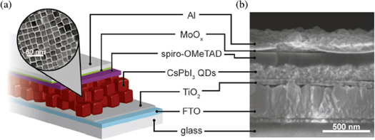
Figure 7. (a) Schematic of the solar cell structure, (b) scanning electron microscopy images of the device. Reprinted/adapted from [221]. © The Authors, some rights reserved; exclusive licensee American Association for the Advancement of Science. Distributed under a Creative Commons Attribution NonCommercial License 4.0. (CC BYNC).
Download figure:
Standard image High-resolution imageThis limitation encouraged the development of bulk heterojunction colloidal QD solar cells, in which the n-type semiconductor and the colloidal QD film are combined in an interpenetrating layer to ensure that photogenerated excitons are formed close to the interface [217]. Unfortunately, this suffered from increased recombination, reducing the photo-voltage. More work is being done to enhance the performance of colloidal QD solar cells, which ranges from material and ligand modifications, to band engineering and passivation, as will be discussed below.
2.3.1. Pb-based QD solar cells
Pb-based QDs, in particular PbS and PbSe, have been very popular choices as sensitizers in colloidal QD solar cells. PbS QDs were used both in the first case of colloidal QD solar cells, as well as high efficiency colloidal QD solar cells reaching 8.55%, because of their excellent absorption properties, which can be tuned from 800 to 2000 nm [222–224]. Furthermore, PbS QDs demonstrate good air stability, which has been a challenge for colloidal QD solar cells. PbSe QDs have also been implemented in solar cells with impressive results, and both PbS and PbSe have demonstrated multiple exciton generation resulting in internal quantum efficiency that exceeded 100%, proving that QD-based solar cells could reach high efficiencies, beyond that of DSSCs [214, 225]. Hot electron transfer from PbSe QD films to TiO2 has also been observed, which can be additionally leveraged for high efficiency devices [226].
Since one of the major limitations of colloidal QD solar cells is charge transport within the QD layer, the conduction characteristics of materials such as PbSe, PbS, and CdSe QD films were investigated to elucidate the processes occurring during device operation. It was found that after exciton dissociation, charge carrier transport occurs through phonon-assisted hopping between the energy levels in QDs, contrary to earlier claims of band-like conductivity [227, 228]. PbS and PbSe QD films have been shown to possess good electrical properties, with PbSe QD films reaching mobilities of 7 cm2 V−1 s−1 after treatment with passivation and infilling [229], which will be re-visited in the next sections.
2.3.2. Improving drift of carriers
The charge carriers inside the QD film are driven by drift currents generated by the electric field in the device [217]. Since carrier transport is below optimal, improvements are needed to enhance the drift of carriers. Efforts have been focused on band engineering and ligand modification to improve charge transport.
Ligand modification has proven key in controlling the electrical properties of QD films. Use of ethanedithiol (EDT) molecules to assist in film fabrication has demonstrated improvement in carrier mobility, associated with reduced inter-particle spacing [230, 231]. But owing to the vulnerability of organic ligands, inorganic ligands were developed to enhance electronic transport and passivate surface defects [232]. Metal chalcogenide complexes were found to result in electron mobilities of 16 cm2 V−1 s−1 in CdSe QDs [233], whereas atomic ligand passivation produced a PbS QD device with efficiency of 6% in the first attempt to fabricate a photovoltaic device with inorganic ligands [232]. In this device, the PbS QDs were capped with oleic acid ligands when synthesized, with thiol treatments removing the oleic acid and passivating the QDs through a Pb–-S bond [232, 234]. The PbS QDs were then treated in CdCl2, tetradecylphosphonic acid (TDPA), and oleylamine (OLA), which improved sized distribution, stability, and reduced defects. Finally, the film was treated with either cetyltrimethylammonium bromide (CTAB), hexadecyltrimethylammonium chloride (HTAC), or tetrabutylammonium iodide (TBAI) to generate halide-passivated PbS QD films.
Apart from ligand modification, band engineering has also been very useful in improving electrical transport in colloidal QD solar cells, involving tuning of the band alignment between the colloidal QD film and the ETL to favor electron injection into the ETL [217]. This has also led to the concept of quantum funnels, essentially the preparation of graded band gap using five QD layers and leveraging the fact that carriers will end up in the layer with the smallest band gap. This has resulted in improved fill factor, open-circuit voltage, and short-circuit current [217, 235, 236]. In addition, graded doping architectures have been used to improve device efficiency [237]. The dopant can be used to tune the conduction band edge and band bending at interfaces, with ligands such as 3-mercaptobutyric acid and EDT used to dope PbS QD films, showing impressive results and leading to record efficiencies [224, 235]. Other efforts have included doping of the metal oxide used as ETL, incorporating impurities in TiO2 and magnesium doping of ZnO, to achieve optimal band offset [238, 239].
2.3.3. Infilling
Another approach to address the limited mobility and conductivity demonstrated by colloidal QD films is infilling with metal oxides. Deposition of Al2O3 and ZnO via ALD to fill the pores of PbSe QD films was observed to reduce the inter-QD tunnel barriers, enhancing carrier mobility [240, 241]. Enhanced conductivity and carrier mobility was also observed after infilling of CdSe QD films with ZnO [242]. ALD appears to be the optimum technique for deposition of the infilling material as it can uniformly coat structures characterized by high aspect ratio, and in work done on infilling a PbSe QD film with amorphous Al2O3, high charge mobility was achieved (7 cm2 V−1 s−1), due to passivation of the QD surface trap states, as well as strong electronic coupling of the sodium sulfide ligands [229]. Furthermore, infilling of a PbSe QD film with Al2O3 or Al2O3/ZnO was observed to result in multiple exciton generation in the QDs, which was not observed in the non-filled films, providing additional motivation for infilling [243]. This is a consequence of the enhanced charge mobility in the infilled films which reduces the possibility of Auger recombination of charges.
2.3.4. Surface passivation
Since the presence of defects hinders charge carrier transport through the QD film and enhances the possibility of charge recombination before they reach their respective contacts, surface passivation to eliminate these trap states can be a useful tool in improving device performance [227]. This can be achieved through different techniques, with ligand passivation being a common method. It was observed that PbS QD films that were treated with 3-mercaptopropionic acid (MPA) demonstrated improved device performance as compared to oleic acid or EDT, associated with superior passivation of defects, leading to higher mobility and minority carrier transport [244]. Infilling is also used to yield improved device stability which is achieved through surface passivation, as it prevents oxidation and photothermal degradation of QDs exposed to ambient conditions [229, 240, 243].
Surface passivation is achieved by exposure of PbSe QDs to chlorine gas, as it results in a thin PbCl2 layer which passivates the QDs and prevents oxidation [245]. PbCl2 can also be used as a precursor for PbSe QDs to create a passivating thin PbCl2 layer [246, 247], or alternatively, treatment of PbSe QDs with NH4Cl can produce a thin PbCl2 layer [248]. In addition, cation exchange techniques have been used to introduce metal cations post-synthesis and enable implementation of techniques used for Cd structures to be used in Pb structures that can ultimately be used to improve carrier transport and reduction of trap states [249, 250] which has been used to passivate PbSe QD films and eventually produce air-stable devices [250].
While many improvements are needed in terms of device stability, conductivity, and performance, colloidal QD solar cells have demonstrated impressive improvements in efficiency since their inception in 2005, reaching efficiencies close to those of DSSCs [221], showing that they are a very promising photovoltaic technology.
2.4. Nanowires
Among nanostructures being actively researched for solar cells, nanowires (NWs) with high aspect ratios and length of 100 nm or more have shown remarkable improvement in PCE compared to their bulk counterparts. Solar cells based on NWs have seen rapid increase in efficiency with PCE values as high as 17% [251, 252], while keeping production costs low. NWs are passive towards impurities present in the bulk, and hence can be fabricated from bulk materials with lower purity, reducing the cost [253]. They help in efficient light management in solar cells through two main methods: (a) by providing spectrally selective improved scattering of light and increased absorption through resonant modes [254–261] and (b) by enhancing charge carrier dynamics through increased efficiency of charge carrier generation and collection [253, 262]. Further, theoretical limit for NW solar cells can reach up to 42% [263], though some have argued that such high performance cannot be attained due to contact and surface recombination [264]. Silicon [258, 265–267] and III–V materials [251, 268–271] are the most commonly studied solar cells possessing NW morphology, although other materials have been studied as well [272]. However, they still have PCE significantly lower than their bulk counterparts and are far from reaching large scale production capabilities. Here, we discuss some key concepts of NW solar cells.
2.4.1. Efficient light management
Scattering of light in NWs is described in terms of wave optics and depends on NW diameter, length, pitch and slant angle [270, 273, 274]. By warrying these parameters it is possible to improve scattering and absorption within a material compared to its bulk counterpart. It is also important to remember that the dependence of these parameters vary with different materials due to differences in their electronic band structure and dielectric properties. Li et al used simulations based on full wave finite element method to show that the hexagonally arranged Si nanopillars with pitch and diameter lying close to 600 nm and 500 nm respectively has increased absorption compared to thin films with the same amount of material [275].
Apart from light scattering, the presence of guided leaky resonant modes are also responsible for increased absorption in nanowires [274, 276]. Multiple studies using analytical waveguide theory have shown that the resonance position of these modes are minimally perturbed from a single NW to sparsely spaced III–V NW array [274, 277], while near field coupling between neighboring NWs is significant in Si NWs [278, 279]. Calculation from Anttu et al showed that these modes had strong diameter dependence and weak dependence on pitch and length in InP NWs with minimal absorption below 100 nm diameter and maximum at 170 and 410 nm respectively [274]. The increase in absorption at these diameters is due to the strong excitation of HE11 (170 nm) and HE22 (410 nm) modes by incident light followed by strong absorption by the NWs. The design of the simulation along with results of which are shown in figure 8. In addition, Dhindsa et al reported that smaller NWs have low absorption at longer wavelengths irrespective of packing density [280], further confirming the dependence of nanowire diameter on performance.

Figure 8. Schematic of the simulation setup used by Anttu et al for InP nanowires. The substrate is of infinite thickness and the space between the wire is filled with air (a) Absorbance spectra for nanowires of pitch 680 nm and length 2000 nm and diameter—100 nm (i), 177 nm (ii), 221 nm (iii), and 441 nm (iv). The light is incident normal to the surface. Reproduced with permission from [274], OSA.
Download figure:
Standard image High-resolution image2.4.2. Charge carrier dynamics
Another important property of NWs is the ability to separate charge carriers near the p–n junction. NWs have significant advantages over bulk materials as the charge carries have to transverse much smaller distances compared to their diffusion lengths, minimizing losses due to scattering and radiative recombination [281, 282]. Some of the important parameters that determine electrical properties of NW solar cells are doping concentration, geometry and surface passivation. In III–V NWs, crystal structure also seem to play an important role in charge separation [264]. Since III–V's can exist in zinc blend and wurzite crystal structure or predominantly as a mixture of the two, such two phase systems can act as scatterers and trap states for radiative recombination [283, 284].
Incorporation of dopants during the growth step on nanowires to create p and n type semiconductor is another important parameter determining the electrical properties of nanowires [285]. In vapor–liquid–solid (VLS), which is the most common growth method for Si NWs, the dopants are introduced as vapor precursors [285]. While the effective incorporation of dopants during growth is still being investigated, the present understanding is that the dopants enter via the seed particle-nanowire interface [285]. In 2009, Nduwimana et al used first principle density functional theory to show charge carrier densities in p and n type doped Si nanowires [286]. Further, Murthy et al used time resolved measurements to show efficient charge carrier separation in Si NWs by having a radial doping gradient [287]. Similar ultrafast charge carrier dynamics studies were also done on GaAs [288] and InP [288, 289] NWs to understand the effect of doping. Some of the recent research on the properties of NWs include charge separation in VLS grown axial nanowires [290], effect of Nb doping and oxygen vacancy centers in TiO2 [291] and ZnO [291–294] respectively.
2.4.3. Device measurements
Due to limitations in fabrication, even with extensive theoretical and experimental study on nanowire optical enhancements and electric properties, it was tough to achieve similar results with device performance [295]. But towards the second half of the last decade, multiple experimental groups have made progress in fabricating structures with results in agreement with theoretical predictions. An image of a working device along with its J–V characteristics are shown in figure 9.

Figure 9. (a) SEM image of the solar cell device. Scale bar 500 nm (b) Schematic representation of the nanowire solar cell device showing different parts of the device (c) Optical microscope image of the solar cell. Scale bar 0.5 mm. The red and the green boxes represent the full device and active area respectively. (d) J–V characteristics of the device at 1 Sun (AM 1.5G) showing PCE, Voc, fill factor and Jsc. The external quantum efficiency spectra of the device from 2250 to 1000 nm [251]. Reprinted with permission from [251]. Copyright (2016) American Chemical Society.
Download figure:
Standard image High-resolution imageSome of the nanowire fabricating techniques will be discussed in brief in the following section, prior to which we need to look the two designs in which we can fabricate a nanowire p–n junction. p–n junction nanowires can be fabricated in both radial and axial direction as shown in figure 10.

Figure 10. Schematic representation of axial (a) and radial (b) p–n junction geometries in nanowire solar cells.
Download figure:
Standard image High-resolution imageIn 2012, it was shown experimentally that radial designs are much less prone to surface defect compared to axial designs though both are capable of maintaining a Voc greater than 0.7 V [296]. It was further confirmed that axial designing of GaAs exhibits large leakage current under backward bias [297]. A radial p–n junction is also ideal for orthogonalization of light absorption and charge carrier collection [281]. However, fabricating a radial NW heterostructure requires precise lattice matching steps and brings up the production costs, while axial designs are passive to any such lattice mismatch strains. Some of the earlier work on coaxial nanowires in 2007 achieved a quantum efficiency of 12% at 690 nm incident light [265] and a PCE of 3.4% in a coaxial p–i–n coaxial silicon solar cell [258]. However, one of the first radial p–n junction solar cells reported a PCE of 12.2% [298] followed by a current density of 40 mA cm−2 in radial Si p–i–n nanowire solar cell [299]. More recently, a hybrid solar cell of Si nanowires and PEDOT:PSS showed a PCE of 13.2% [300]. Apart from Si, there have been various experimental realizations of III–V nanowire solar cells. In 2013, radial GaAs nanopillar solar cells with 70% quantum efficiencies and 63% fill factors were reported [301]. Even though axial design has a disadvantage over radial design, some of the highest recorded efficiencies have been reported for axial nanowires. Axial GaAs nanowire solar cells in 2015 demonstrated a record efficiency of 15.3% [269] in well over the previous highest value of 13.8% in InP nanowire solar cells [302]. This value was exceeded in coaxial InP NWs with the help of self-aligned nanoparticles which helped in improved absorption, with a reported a PCE value of 17.8% [251]. Similar high performance solar cells have also been reported for CdS [303–305], ZnO [306, 307], Cu2O [306] and more recently, for perovskite nanowires [271]. Research has also begun into tapered NW structures like nanocones [308] and dual-diameter tandem NW solar cells [309]. Such structures help reduce reflectance while maximizing effective absorption.
2.4.4. Fabrication techniques
For the realization of efficient light management and enhanced PCE in nanowire solar cells, it is of paramount importance to develop low cost, precise and reproducible fabrication routes. In the section we will look at different growth methods employed for nanowires (mostly Si and III–V's). Since several detailed reviews on nanowire growths are available [310–313], the discussion is intended as a brief overview with some recent advances made.
VLS method is a growth mechanism in 1D materials known for than more than 50 years [314] and is the most common technique used for the growth of Si and other semiconductor nanowires. They are cheap and can grow single crystal nanowires with high crystallinity [281, 282]. The process involves passing a vapor of the precursors on a substrate with a solid seed nanoparticle, generally gold, at very high temperatures (500 °C–1000 °C) [315, 316] in the presence of a liquid catalyst. The liquid catalyst is formed during the initial phase, when the precursors dissociate to form a metal-nanoparticle droplet, that on further addition of dissociated precursor, leads to nucleation sites at its surface. SiH4, disilane, SiH2 and SiCl4 are the most commonly used source gasses for Si [317]. In 2009, growth of GaAs nanowires was demonstrated via VLS in a gas source molecular beam epitaxial system [295]. Another advantage of VLS is the ease of growing p–n heterostructures by passing different doping gases along with the source gases. One of the earlier uses of VLS growth mechanism was to grow Si nanowires using chemical vapor deposition (CVD) technique [316]. They further demonstrated patterned growth of nanowires using Au colloidal seed particles. CVD [315, 316] and molecular beam epitaxy techniques [318, 319] are two of the common fabrication routes that uses VLS mechanism for aligned single crystalline growth of nanowires. The 17.8% efficiency reported in nanowires were grown using VLS [251]. However, it must be noted that multiple other factors like plasmonic enhancement played an important role in the high efficiency reported.
Metal organic chemical vapor epitaxy (MOVPE ) is predominantly used for III–V nanowire growth as initial results of GaAs nanowire solar cell grown using VLS showed very low efficiencies, less than 1% [295]. Though multiple reports on InP nanowire growth using MOVPE existed [320–323], the first InP nanowire solar cell, based on the method was reported in 2009, and showed an impressive PCE of 3.37% [324]. In the case of GaAs, it was not until 2012, that an impressive PCE of 2.54% was reported in densely packed uniform GaAs nanowires [301]. Further, the same group improved on the efficiency to 6.63% in 2013 [325] by making use of surface passivation techniques. Since then, multiple reports showing high efficiencies in GaAs [252, 268] InP [251, 302] have been reported. The MOCVE technique involves a combination of electron beam lithography and vapor epitaxy to grow nanowires of uniform thickness and shape [301]. The first step involves deposition of lithographically patterned SiO2 mask with an array of holes onto a p-type substrate of the nanowire material. This is followed by chemical vapor epitaxial growth of the nanowire though the etched out holes, followed by growing the n-type shell on the p-type nanowires, by varying the growth conditions. The process involves elevated temperatures in the range of 600 °C–800 °C. Figure 11 shows InAs nanowires gown using MOVPE.
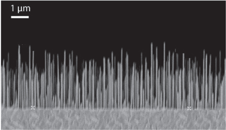
Figure 11. SEM image of MOVPE grown lnAs nanowires. Reprinted with permission from [323]. Copyright (2013) American Chemical Society.
Download figure:
Standard image High-resolution imageMost of the growth techniques mentioned above are based on bottom-up methods. Many top down synthesis routes also exist for the fabrication of nanowires, although, challenges exist due to the need for high precision and throughput production. In 2005 a growth technique was developed for single Si nanowire using aqueous electroless etching method, involving etching a Si wafer using HF acid followed by deposition of a-Si using disilane gas at 450 °C [326, 327]. This synthesis technique was made use of to test a Si nanowire solar cell which reported a low efficiency of 0.5% [328]. The most common type of wet etching—metal assisted chemical (MAC) etching involves a noble metal nanoparticle covering the Si wafer followed by reaction with an etchant [329–331]. The etchant facilitates oxidation of the Si wafer beneath the metal and as the process progresses, the Si beneath the metal nanoparticle is etched away forming Si nanowires [282]. This method is cheap, and can be used for mass production of isotropic nanowires. The etching technique was further improved upon with the addition of template assisted MAC etching [327, 332] as shown in figure 12. This technique offers better control over density, shape and length of the nanowires. MAC technique is still popular for the growth of nanowires and results have shown comparable solar cell efficiencies [333, 334]. Apart from wet etching, a number of dry etching techniques such as laser ablation [335], reactive iron etching [336], plasma etching [337] and chemical assisted ion beam etching [338] also exist for nanowire growth.

Figure 12. Schematic and corresponding SEM images of ordered nanowires arrays formed through metal assisted chemical etching. (a) A mono layer of silica colloidal crystal is deposited on the silicon substrate. (b) Silica crystal template is then sintered at 1273 K for 80 min followed by etching using 50:1 HF to form 2D array of non-close packed silica colloidal crystal. (c) Silver is deposited on the silica through conventional vacuum vapor deposition. (d) silver coated silica is then lifted through ultra-sonication for 2–3 min to form a 2D metal arrays of silver. (e) The ordered array of SI nanowires is formed from etching using HF. The corresponding SEM mage of each step is shown on the right side of the figure. Reprinted from [332], with the permission of AIP Publishing.
Download figure:
Standard image High-resolution imageThe above discussed methods are the common techniques for growth of nanowires, but there have also been reports of various improvements on existing techniques to show high efficiencies. MOCVD was used to report a PCE of 8.8% in graphene/single nanowire Schottky junction solar cell [339, 340]. Nanowire solar cells with efficient light management has the capability to outperform their bulk counterparts both in efficiency and cost. Due to fabrications limitations, material quality and poor design they are yet to achieve efficiencies close to their theoretical predictions. But the last few years have seen substantial improvement in nanowire solar cells and shows great promise to improve further in the next few years.
3. Photon management
In the previous section we discussed how different types of active materials can help to enhance efficiencies in solar cell technologies. Improvements of even a few percentages are considered respectful when it comes to photovoltaics. Hence, scientists over the past few decades have started to look beyond materials improvements and focused a substantial effort on improvements through incorporation of plasmonic nanostructures [341–343], and up- and down-conversion materials with the PV medium. Enhancement in solar cell performance can occur either through improved light management such as absorption due to localized electric fields, or by efficient use of the solar spectrum via hot electron injection and up/down conversion (UC/DC). In this section, we will briefly review the role of plasmonics and UC/DC materials in photovoltaic enhancement.
Plasmons are quasiparticle excitations of electrons in metals due to interaction with electromagnetic waves. Such excitations are not observed within the bulk of the material where the plasmon and photon dispersion curve do not intersect, however propagating plasmons are possible near the surface of the metal and are aptly called surface plasmon resonances. Metal nanoparticles having a size much smaller than the wavelength of visible light, allowing electric fields to propagate within the volume and resulting in plasmon excitations that are localized on the nanoparticle, producing waves of collective electron oscillations called Localized surface plasmon resonances (LSPR). LSPR have finite lifetimes and decay either radiatively or non-radiatively. The radiative decay leads to near and far filed scattering effects, while non-radiative decay leads to hot carrier generation and plasmon resonance energy transfer (PRET). A number of reviews detailing theoretical and experimental reviews on plasmon resonance on metal nanoparticles such as Au and Ag are available [344–348], hence in this section we will not be dwelling on the details of LSPR theory, but rather focus on its use in enhancing PV performance.
Though surface plasmons have been studied since the 1950s [349], it was only towards the end of the 20th century that it got a major boost in materials science due to improved fabrication techniques. In 2000, the term 'plasmonics' was coined, predicting a new class of devices based on surface plasmons [350]. Around 2004, multiple groups in parallel demonstrated charge transfer from metal nanoparticles to semiconductors using LSPR [351–353]. This led to a major boom in the field of plasmonics with extensive research being carried out on the use of this aspect in photo catalysis [354–356], drug delivery [357, 358], nanoscale wave guides [358, 359], circuits [360–362], optical emitters and antennas [363–365]. Almost immediately, plasmonic nanostructures (PNs) were tested for improving existing high efficiency photovoltaic technologies including silicon [366–370], DSSC [369–373], GaAs [374, 375], and recently, even perovskite solar cells [376, 377].
3.1. Plasmonic nanoparticles based solar cells
There has been a steady increase in published work on PN-based solar cells since 2006 [378]. Improvements in performance of DSSC, Si and perovskite solar cells on incorporation of PNs have been reported. Au and Ag are the most commonly used nanostructures in plasmonic solar cells, as their plasmon resonance wavelength lies within the solar spectrum. Their high stability and relative ease in synthesizing anisotropic structures also aid in incorporating them into different sensitizer materials. Materials like Ti [379], Al [380], and Cu [381, 382] have also been tested with reasonable success. In photovoltaics, PNs are mainly used in different configurations alongside the active material of a solar cell as shown in figure 13 [341]. They improve the performance of the solar cell through (a) enhanced absorption due to multiple scattering mechanisms (b) enhancement charge carrier separation from localized high electric fields (c) Plasmon assisted hot electron injection and (d) PRET between the active material using plasmonic nanostructures. The schematics of these mechanisms can be seen in figure 14 [342]. We will discuss these mechanisms in detail in the following subsections.

Figure 13. Schematic representation of different designs of plasmonic solar cells. (a) nanoparticle on the front of the solar cell using far field scattering to enhance absorption (b) PNs are incorporated into the active material for near field scattering effects and non-radiative plasmonic processes like HEI and PRET. For PRET, the PNs will have a dielectric coating to prevent interfacial recombination. (c) Patterned back metal contacts for propagating surface plasmons at the metal semiconductor interface for efficient light absorption. [341] (2010) Copyright © 2010, Springer Nature. With permission of Springer.
Download figure:
Standard image High-resolution image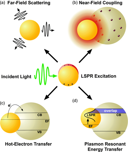
Figure 14. Schematic representation of different plasmon enhancement mechanisms used in solar cells. (a) and (b) are near and far field scattering respectively. (c) and (d) represent non-radiative coupling using hot electron transfer and PRET. Reproduced from [342]. CC BY 3.0.
Download figure:
Standard image High-resolution image
Figure 15. Schematic representation of hot electron transfer mechanism. (a) Excited plasmons decaying via radiative emission of photons or non-radiatively by exiting hot electrons in the metal. Localized surface plasmons can decay radiatively via re-emitted photons or non-radiatively via excitation of hot electrons in the conduction band. (b)Hot electron having energy above the Fermi level (c) Hot electrons can be transferred to the semiconductor if the electrons have energy greater than the Schottky barrier of the metal-semiconductor junction. φM is the work function of the metal and χS is the electron affinity of the semiconductor. [343] (2014) Copyright © 2014, Springer Nature. With permission of Springer.
Download figure:
Standard image High-resolution image3.1.1. Enhanced scattering in plasmonic solar cells
3.1.1.1. Far field scattering
For enhanced far-field scattering, the metal nanoparticle is generally placed in the front side of the device, at the interface between air/dielectric and the active material. Mertz et al had shown that although light scattering is symmetrical in a uniform medium, when placed at an interface, there is preferential scattering towards the material with higher permittivity [383]. This in turn increases the optical path length of solar radiation due to angular dispersion and total internal reflection resulting in enhanced absorption. Additionally, the scattered light can encounter nearby nanostructures, additionally increasing the percentage of trapped light. It is also important to note that the scattering cross section of the nanoparticle can be much bigger than its physical cross section, thus reducing the amount of nanoparticle required [341].
Shape, size and dielectric medium are key factors that lets you tune scattering cross section and LSPR frequency of the metal nanoparticle [373, 384–386]. Since scattering cross section scale as the square of the volume, and ohmic losses is proportion to the volume, larger Ag and Au nanoparticles are preferred for large field scattering. The most common morphology utilized for achieving far field scattering in solar cells is by distributing the nanoparticle on top of the thin film. In 2006, 100 nm Au nanoparticles were used on top of amorphous Silicon solar cells, and an 8.1% increase in short circuit current was observed [387]. A similar increase in short circuit current was observed in GaAs solar using 110 nm Ag nanoparticles [369]. Catchpole and Polman numerically calculated the amount of light scattered for different nanoparticles and reported higher scattering for a cylinder or a hemisphere over spherical particles [388]. They further saw that the scattering cross section can be tuned effectively by adding a spacer above the substrate. A 45% enhancement in short circuit current was achieved by using metallic arrays on top of thin films [389]. Fabricating a plasmonic layer in front of the device for far field scattering is relatively straightforward, as a result encouraging such a design for plasmonic solar cells. However, the improvements observed are relatively below par. Consequently, for plasmonic solar cells to demonstrate significant improvement, multiple plasmonic enhancement mechanisms must occur in parallel.
3.1.1.2. Localized field scattering
Absorption is also enhanced within the local vicinity of the plasmonic nanoparticle due to near field enhancement of electric fields resulting from localized surface plasmons. In such plasmonic solar cell designs, metal nanoparticles are embedded into the active material as shown in figure 14(b). At resonance, the electric field around the nanoparticle can be orders of magnitude higher than the incident electromagnetic spectrum, thereby creating a small region of concentrated photon flux than can be absorbed by the semiconductor, creating an additional fraction of electron hole pairs [341, 342, 390, 391]. These effects become prominent near the LSPR frequency, which can be tuned by adding a dielectric spacer between the nanoparticle and the active material. For example, in 2009 an increased absorption in Si solar cells was observed with the use of Ag nanoparticles whose resonance could be tuned up to 200 nm with the use of dielectrics SiO2, TiO2 and Si3N4 [392]. Further, FDTD simulations have showed that structures with sharp edges enhance electric fields much more than smooth surfaces [393–396], hence anisotropic structures such as rods [397], cones [398], bowties [390], etc have been tested extensively for enhanced near field effects.
Several groups have reported enhancement in PV performance based on incorporation of plasmonic nanoparticles into the active material of the device. It must be noted that these enhancements also have significant contributions from non-radiative effects. In 2008, electrodeposited Ag nanoparticles were used which resulted in an improvement in PCE of organic solar cells [399]. A similar improvement in polymer heterojunction solar cells was observed using Au nanoparticles [400]. Both these results primarily originated from the concentration of electric fields near the nanoparticles. Multiple reports of enhancements in DSSC by integrating metal nanoparticles with the mesoporous TiO2 layer have been reported [401–405] as well. A systematic study of the effect of size of Au nanoparticle on DSSC performance found a maximum efficiency using 36 nm Au [406]. Similar enhancements were reported for perovskite solar cells in which a core shell Au nanoparticle was incorporated with the perovskite thin film [407]. They argued that a reduction in exciton binding energy as a result of coupling with the LSPR was responsible for the improved efficiency. Another technique to improve absorption is using the back metal surface that facilitates the propagation of surface plasmons at the metal-semiconductor interface. Since these do not closely lie within the scope of this article, we will not be discussing it in detail.
3.1.2. Non-radiative effects
3.1.2.1. Hot electron injection (HEI)
In addition to enhancement through efficient absorption, recent investigations proved that it is possible for plasmonic nanostructures to transfer hot electrons from the metal directly into the conduction band of the semiconductor [164]. Hot electrons refer to electrons that have gained kinetic energy from an external electric field and are no longer in thermal equilibrium with the atom, hence are described by Fermi statistics with an elevated temperature. Schematic and band diagram of hot electron transfer is shown in figure 15 [343]. Many existing PV technologies such as DSSC, quantum dot solar cells and quantum dot-sensitized solar cells have previously utilized HEI to further improve their power conversion efficiencies [164, 408, 409]. Around 2004–2005, several groups reported on the ability of plasmonic nanostructures to generate 'hot electrons' under illumination, and these led to major progress in photo-catalysis and photovoltaics [346–348]. Hot electrons in metal nanoparticles are generated as a result of non-radiative decay of localized surface plasmons. LSPR excitation decay occurs on a time scale of femtoseconds with the emission of radiation or non-radiatively by transferring the energy to hot electrons, which can undergo photoemission, if its energy exceeds the work function of the material. A fraction of the energy is also lost as heat, but as mentioned above, ohmic losses are lower in Au and Ag. Probabilistically, majority of excited electrons originate from intraband excitations within the conduction band compared to interband excitations, as the d band energy levels lie 2.4 and 4 eV below Fermi level in Au and Ag, respectively [343].
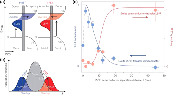
Figure 16. (a) Band diagram comparing FRET and PRET mechanisms along with the direction of energy transfer in both (b) spectral overlap between donor and acceptor in FRET and PRET. (c) Distance dependent dipole–dipole interaction in FRET and PRET. 1 in FRET means no energy transfer from semiconductor to metal and 0 means the semiconductor is fully quenched. 1 in PRET refers to full energy transfer between the plasmon and the semiconductor while 0 means no energy is transferred. [410] (2015) Copyright © 2015, Springer Nature. With permission of Springer.
Download figure:
Standard image High-resolution imageThe excited hot electrons can thus escape the nanoparticle and can be injected into the conduction band of the semiconductor by forming a Schottky junction. Note that this mechanism becomes efficient only if the energy needed for such injection is lower than the band gap of the active material. Even with a perfectly absorbing plasmonic nanostructure, the PCE enhancement through HEI is limited to <8% [411]. However, modifying the electronic density of states of the donor and acceptor could help improve upon this value.
One of the first comprehensive studies of HEI came from observation of photo-induced electron transfer between Au and thin film and nonporous TiO2 [346]. Shortly afterward, multiple results observing electron diffusion between metal nanoparticles and TiO2 were published [412–415]. Some of the recent results of HEI in PV include using HEI in sandwiched TiOx–Au–TiOxto improve efficiency in perovskite solar cells [416], improving NIR absorption in Si solar cells using Ag nano arrays [417], independent plasmonic solar cell with 0.2% PCE [418] and solid state ITO∣Au-NPs∣TiO2 solar cell with 5.84% photon to electron conversion rate at 700 nm incidence [419]. HEI using plasmonics have shown the ability to increase population of electron hole pairs in solar cells, but their performance have been limited by the fraction of the hot carriers having energy to cross the Schottky barrier and various hot electron relaxation pathways [420].
3.1.2.2. Plasmon resonance energy transfer
PRET or plasmon induced energy transfer, is the non-radiative energy transfer between a plasmonic nanoparticle and a semiconducting material via dipole–dipole coupling. Upon illumination of resonant light, the excited plasmon decays by transferring energy to the semiconducting material, thus creating extra electron hole pairs near its conduction band edge [410]. The metal and the semiconductor is separated by an insulating layer such as SiO2 to prevent interfacial recombination or losses due to hot electron transfer. The large dipole moment in plasmons arise from coherent oscillation of the conducting electrons. An efficient PRET system can improve the performance of solar cells by utilizing light below the band gap. A major drawback of PRET is that it competes with Forster resonance energy transfer (FRET), i.e. an efficient FRET system implies an inefficient PRET system. The two competing energy transfer mechanisms are shown in figure 16 [410]. The efficiency of either system is determined by the dephasing time of the plasmons, versus that of excitons, in the semiconductor. When the excitons have a lower dephasing time, energy is transferred to the semiconductor from the plasmonic particle (PRET), while the reverse energy transfer (FRET) is favored when the plasmon has a low dephasing time. It was experimentally demonstrated in the same study that in Au@SiO2@Cu2O, a separation of greater than 10 nm between the Au and Cu2O results in no PRET [410].
Most studies on PRET are fairly recent, and have been focused on understanding plasmon dephasing times using optical spectroscopic techniques such as interferometric frequency resolved optical gating [421]. Over the last 3 years, PRET has found application in sensing, photo catalysis and photovoltaics [351, 422–424]. High photocurrent density was reported in Ag@Ag2S sensitized thin film solar cells, attributed to both PRET and HEI mechanisms [425]. It is quite possible that while PRET has been delved into only recently, earlier enhancements reported had contributions from PRET, particularly in the near field scattering designs. Over the last decade, rapid development in plasmonics have shown promising results in photovoltaics. Though, initially plasmonic nanostructures made their foray into solar cells for their improved scattering capability, recent findings have presented their ability to non-radiatively couple to semiconducting materials, presenting a case for additional enhancements. Nevertheless, further improvements in plasmonic solar cells demands parallel designing of novel nanostructures as well as their integration of them into the solar cells.
3.2. UC and DC materials
In order to exceed the Shockley–Queisser limit for single junction solar cells, two other possible methods commonly employed are UC and DC processes. This is achieved by reducing losses due to transparency and lattice thermalization, two major loss mechanisms in single junction solar cells. Transparency is where any photon of lower energy than the band gap is not absorbed by the material, whereas lattice thermalization is when a photon of higher energy than the band gap is absorbed to create and electron–hole pair with the excess energy is released as lattice vibrations to the material. Both UC and DC are non-linear optical process that convert two photons to a single photon and a single photon to two photons respectively.
The multiple forms of energy losses in a single junction PV include '(1) Non absorption of light with energy lower than the band gap (2) Energy loss due to lattice thermalization (3) Junction loss (4) Contact loss and (5) loss due to recombination' [426]. Other major mechanisms leading to losses in solar cells are radiative losses from recombination of electrons and holes and from voltage drop across junctions and contacts [427–429]. One of the major advantages of the UC and DC methods of improving PV efficiency is that it can be implemented to existing single junction PV, without adding any additional fabrication techniques to avoid current mismatch losses as in the case of tandem device [430, 431]. These UC and DC layers are optically passive, while current collection architecture remains the same as in a single junction PV device. In the case of UP the layer is added to the rear end of the device to convert two low energy photons to a higher energy such that the emitted photon has an energy greater than the band gap of the material [432, 433], while in DC, the optical layer is at the front of the device as they convert a higher energy photon to lower energy. The effectiveness of UC and DC depends on the band gap of the material used in the solar cell. For example, crystalline silicon (c-Si) has a short band gap of 1.12 eV and can utilize a large portion of the long wavelength region of the solar spectrum, while hydrogenated amorphous silicon (a-Si:H) has a larger band gap of 1.7 eV and makes use of the shorter wavelength in the spectrum, while being transparent to most near infra-red light [427]. It is easy to see that UC will be more beneficial for a-Si:H compared to c-Si. The schematic of an upconverter and a downconverter solar cell is shown in figure 17.

Figure 17. Schematic representation of the solar cell with up and down conversion layers added on them.
Download figure:
Standard image High-resolution image3.2.1. Up conversion materials
UC is an anti-Stokes process, can be done at low power, does not require highly coherent light and can be achieved even using Xenon or Halogen lamps [434–436]. The underlying principle of up conversion can be understood from figure 18. Energy is absorbed from the ground state and electrons are carried to their first exited state. The first exited state is a metastable state and require a relatively long lifetime for the UC process to work. Consequently, another photon is absorbed and now the highly populated metastable state is exited to the higher energy state, followed by radiative recombination to the lowest energy state [429, 437]. During the whole process two photons of lower energy were absorbed and a photon of higher energy was emitted.
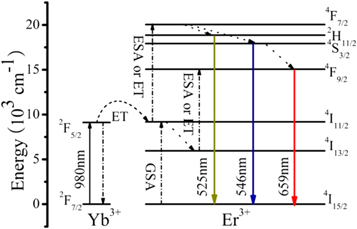
Figure 18. Schematic representation of energy level diagram in NaYF4:Yb3+,Er3+ nanoparticles. The arrows indicate the up conversion process. Reprinted with permission from [438]. Copyright (2014) American Chemical Society.
Download figure:
Standard image High-resolution imageThe most common materials used for up conversion processes are lanthanide nanoparticle based luminescence [427–430] and triplet triple annihilation based on organic molecules [427, 439]. In this article, we will focus on the lanthanide nanomaterials for up conversion. Although the basic energy scheme remains the same, there are multiple ways to achieve up conversions and the most effective way is to use an energy transfer up converison, in which a host material is responsible for transferring energy to the activator nanophore. The first energy transfer excites the activator to the metastable state, this can either be followed by another energy transfer or the activator absorbs the next photon to reach the excited state [440, 441]. Similarly, there are other pathways to achieve such energy transfers [442, 443]. The advantage of using energy transfer up conversion is that we do not require a high concentration of activator ions [440].
The host is generally an inorganic molecule with minimum non-radiative losses. Researchers have studied various host matrices including fluorides [444–446], other halides [447], oxides [448, 449], and phosphates [450, 451] etc. For lanthanide nanoparticles, NaYbF4 is the most common used host. However, using Gd2O2S [452–454], BaY2F8 [455, 456] and fluorozirconate glass [457, 458] as host material is also common. Er3+ [431, 434, 445, 452, 454–456, 459], Tm3+ [447, 450, 460], and Ho3+ [460, 461] ions, with their appropriate f electron configurations, nearly evenly spaced energy levels and long excitation lifetime, are commonly used as the activator material. The three step UC in Er3+ energy levels are shown in figure 18 [438]. The larger absorption cross sectional area in Yb3+ ions compared to activator along with their convenient relaxation energy, which resonates with the excitation energies of activator ions are major factors in improving the efficiency of the energy transfer UC [436].
The first proposed use of UC was in 1982 using terbium-doped lanthanum fluoride and thulium-doped calcium tungstate [437], followed by the first demonstration in 1996 of an improvement in GaAs solar cell performance using co-doped Er3+ and Yb3+ [462]. Over the years, different solar calls have been tested using various lanthanides as dopants. In 2002, a theoretical prediction was made of a PCE of 47.6% in c-Si solar cells using sub-band gap light, considerably higher than the Shockley–Quessier limit [463]. Erbium-doped sodium yttrium fluoride (NaYF4:Er3+) as the host-activator matrix achieved an internal quantum efficiency of 3.8% in c-Si solar cells at laser excitation of 1523 nm [459]. In 2009, Gd2(Mo04)3:Er3+ was proposed as an up conversion phosphor for Si solar cells [464], but it was only in 2010, that UC was finally tested in organic and DSSCs, with the use of Er3+,Yb3+ co‐doped LaF3‐TiO2 nanocomposites as a middle layer in DSSC to produce an improved PCE of 2.69% [465]. Yttrium fluoride host doped with erbium in P3HT:PCBM solar cell showed a four-fold increase in photocurrent at 975 nm illumination [466]. With silicon solar cells, some of the recent works involve improved external quantum efficiencies at long wavelength irradiance and approaches into NIR broadband UCs [467, 468].
Some of the recent works on up conversion in PV are summarized in table 1.
Table 1. Recent studies on up converison materials for improved solar cell performance.
| Material | Comments | Year |
|---|---|---|
| NaYF4:Yb/Er up conversion nanoparticles | PCE in Perovskite solar cells increased from 17.8% to 18.1% upon NIR irradiation | 2016 [469] |
| Er3+-doped β-NaYF4 | Si solar cells—internal and external PL quantum yield of 10.7% and 6.6% at 980 nm | 2014 [470] |
| BaY2F8:30% Er3+ | Si solar cells—external quantum yield 8% at 1520 nm and 0.55% relative efficiency increase | 2015 [471] |
| NaYF4:Yb,Er/Li-Ag@SiO2 | Co-enhancing effect between up converison and LSPR. | 2017 [472] |
| NaYF4:Yb3+, Er3+@SiO2,@Au,@TiO2 | Enhanced up converison efficiencies in NaYF4:Yb3+, Er3+ prisms due to LSPR in Au nanoparticles | 2016 [364] |
| Er3+-Yb3+-Li+ tri-doped TiO2 | PCE in Perovskite solar cell increased from 14% to 16.5% | 2018 [473] |
| Cylamine sensitized NaYF4:Yb,Er nanoparticles | Broadband NIR up conversion. | 2012 [474] |
| Up conversion efficiency enhanced by a factor of ∼3300 |
3.2.2. DC materials
Losses due to thermalization can be reduced with the use of DC materials that help in generation of multiple electron–hole pairs for incident photons of energy greater than twice the band gap of the material. Hence, DC is more beneficial for solar cells with smaller band gaps as it converts a photon of higher energy to two photons of lower energy, implying an external quantum efficiency of 200%. Although a DC layer is typically applied to the front surface of a solar cell, it is possible to add a rear layer in the case of bifacial solar cells [427, 428]. It was theoretically predicted that a conversion efficiency of 38.6% can be achieved in c-Si solar cells attached to an ideal DC convertor under un-concentrated light, by increasing the available spectral irradiance by 32% [475].
DC works in materials with an intermediate state between their bands. It was shown that in such materials, under low light intensity such as concentrate light, absorption occurs via band to band transition, while radiative recombination occurs with the help of an intermediate level [475]. However, another way to achieve such DC is through cooperative energy transfer between ions, achieved through co-doping two different ionic systems in a material [476, 477].
In 2005, a cooperative energy transfer efficiency of 88% was reported in (YbxY1−x)PO4 doped with 1% Tb3+ upon excitation using a Xe lamp [478]. As expected, the energy transfer in DC occurs opposite to that of UC, that is, from two Tb3+ to one Yb3+ ion. Around the same time, multiple groups also reported improved PCE and short current density in c-Si solar cells with the use DC materials [478]. Broadband DC of UV light resulting in emission of NIR photons upon excitation using was reported in 2008 with a high energy transfer efficiency of 74% between Ce3+ and Yb3+ ions co-doped in borated glasses [479]. Further, they reported a DC of visible light at 475 nm in a co-doped system of Yb 3+ doped oxyfluoride glass ceramics with precipitated TbF3 nanocrystals [480]. Other commonly used materials for down conversion are CdO nanotips [481], ZnO:Er3+/Yb3+ [482], GdAl3(BO3)4(Pr,Tb)3+,Yb3+ [483], YF3 doped with Pr3+ Yb3+ [484], Gd2O2S:Tm3+ [485], and lanthanide ion doped glasses [486]. Many groups have reported improved performance in solar cells with DC materials, and some of the recent results are shown in table 2.
Table 2. Recent studies on down conversion materials for improved solar cell performance.
| Material | Comments | Year |
|---|---|---|
| ZnO: Eu3+, Dy3+ | <200% improvement in current density and PCE in DSSC compared to using TiO2 alone | 2014 [406] |
| Eu and Tb coordination complexes | On spin coating DC coordination complexes onto Si solar cell, a maximum relative increase in PCE by 8% | 2016 [407] |
| Lanthanide ions doped into Metal organic frameworks | PL, absorption and NIR emission enhancement | 2018 [408] |
| Graphene quantum dots | Improved fill factors and short circuit current, achieving a PCE of 16.55% in Si heterojunction solar cells | 2016 [409] |
| Ce and Yb doped Perovskite quantum dots—CsPbCl1.5Br1.5:Yb3+, Ce3+ | PCE improved from 18.1 to 21.5% in Si solar cells | 2017 [164] |
| CuInS2/ZnS core shell quantum dots | 10.5% relative PCE improvement in Si solar cells | 2014 [411] |
Over the last decade active research on UC and DC materials have helped in improving the efficiencies of solar cells. However, the reported values are still low and demands testing new materials and better fabrication techniques. Researchers have also tested plasmonic and photonic materials as efficient UC/DC materials [487, 488]. These materials have additional benefits of enhanced scattering and other plasmonic effects described earlier. Another approach is the use of concentrated light source [427, 489]. UC/DC are yet to achieve substantial improvements that can be implemented into existing commercial devices. However, over the last decade, encouraging results with an increasing trend in efficiencies is visible.
4. Nanomaterials beyond PV
The properties of nanomaterials that make them well-suited as active materials in photovoltaic devices (broadband absorption, high quantum yield, etc) also make them ideal candidates for LSCs. These devices also harvest solar energy, but instead of directly allowing charge generation, they act as down converters for other PV cells. LSCs are economically more viable than PVs and have the additional advantage in that they may be incorporated in to existing PV modules to improve performance. Further, they are far better candidates as building incorporated photovoltaic (BIPV) platforms, given they function under both direct and diffuse light. We will review dye, thin film, and quantum dot based LSCs that have garnered a lot of attention in recent years as these devices face a resurgence given the advances in materials science and engineering which have led to novel QDs and hybrid semiconductors.
LSCs are usually made from some transparent layer, typically a polymer thin film, which is doped with a fluorescent species, such as dye molecules or quantum dots, among others, that are responsible for absorbing sunlight and re-emitting at a longer wavelength [490, 491]. The emitted light is then trapped in the LSC due to the high refractive index of the transparent layer and via total internal reflection it is waveguided to the edges of the LSC, where an attach solar cell converts the light to electricity, as shown in figure 19. Therefore, a good LSC material should demonstrate a broad absorption spectrum, minimal overlap in its absorption and emission spectra (i.e. minimal Stokes' shift) to prevent re-absorption of the emitted light, high quantum yield, and emission should match the absorption of the attached solar cell [490]. In the effort to optimize all aspects of the LSC, various materials were investigated as possible fluorophores.

Figure 19. Operating principle of LSCs.
Download figure:
Standard image High-resolution image4.1. Organic dye-based LSCs
Organic dyes were considered in the original design and used as the fluorophore in the first LSCs, as they offer good solubility in solvents, high quantum yield, and good absorption spectra [490, 492–494]. Since then, extensive work on various types of dyes has yielded a large amount of potential dyes. These include dicyano methylenes, lactones, bipyridines, coumarins, rhodamines, porphyrins, phtalocyanines, and perylenes, as well as many others, among which coumarines, rhodamines, and perylenes have been particularly popular [490]. Rhodamines were used since early work on LSCs due to their high quantum yield, but suffer from small Stokes' shift, which results in significant losses due to high re-absorption [492, 495]. Furthermore, the Rhodamine 6G fluorescence was reduced after incorporation in a polymer [496], whereas various rhodamine dyes demonstrate poor photostability [497, 498]. This encouraged investigation of alternative dyes. Coumarins show a larger Stokes' shift and quantum yields of up to 98% have been observed [498–500]. Furthermore, they exhibit superior stability, although they are still lagging in comparison to other dyes. Perylene dyes are characterized by bright fluorescence and good stability after modification with cyano side groups, reaching quantum yield of 91% [501]. Perylene derivatives, such as perylene bismides, show very bright fluorescence and good stability, but suffer from low solubility, which is improved by addition of ortho-alkylated aromatic bulky groups [490, 502]. Moreover, perylene dyes have been engineered to demonstrate Stokes' shift of up to 300 meV [503]. As perylene dyes show such good properties, multiple dyes can be combined in LSCs to achieve good absorption and quantum yield simultaneous [504]. Dicyano methylene dyes have also shown good properties for implementation in LSCs. DCM (4-(dicyanomethylene)-2-methyl-6-(p-dimethylaminostyryl)-4H-pyran) possesses a broad absorption spectrum and large Stokes' shift, while its quantum yield can reach 80%, but it suffers from poor photostability [490, 496, 499]. DCJTB (4-(dicyanomethylene)-2-t-butyl-6-(1,1,7,7-tetramethyljulolidyl-9-enyl)-4H-pyran) combined with a platinum-porphyrin dye yielded a device with efficiency 6.8% when attached to a GaAs solar cell [505].
Other well performing dyes include CRS 040 yellow (coumarine dye) and Lumogen red (perylene dye) [506, 507]. Combination of these two dyes in a LSC attached to a GaAs solar cell has generated the highest PCE using an LSC to date, reaching 7.1% [508]. Due to the limited absorption of organic dyes, combination of dyes, either in a single device, or in a stack of devices, can be used to leverage the absorption spectra of multiple dyes [490]. In addition, multiple efforts to improve stability of organic dyes have encompassed introduction of UV absorbers to prevent degradation under UV light, and use of copolymers to improve photostability [490, 509].
4.2. Quantum dot based LSCs
Due to the issues faced by dyes, such as rapid degradation and limited absorption by a single dye, QDs have risen as a potential alternative to dyes as fluorophores in LSCs, since the absorption spectrum of QDs can be easily manipulated to match that of the solar spectrum [510], whereas their composition of mostly inorganic semiconductors prevents rapid degradation [511]. Moreover, by appropriate combination of QDs of different sizes, LSCs with significant Stokes' shift can be fabricated [512, 513].
Common colloidal QDs that have been used in LSCs include CdS, CdSe/CdS, CdSe/ZnS, and PbS/CdS, among others [490, 491]. Work has been done to understand how each of these behaves in a LSC and how they can be optimized. Comparison between the properties of PbS QDs and CdSe/ZnS QDs in solution has shown that PbS QDs demonstrate a much larger Stokes' shift of 122 nm, as compared to 23 nm for the CdSe/ZnS system, as shown in figure 20(a) [514]. Nevertheless, PbS QDs are found to possess a much lower extinction coefficient than CdSe/ZnS. On the other hand, a study on Cd-based QDs has indicated that despite the decreased absorption coefficient for NIR-absorbing QDs, they still have a better absorption efficiency compared to QDs that only absorb in the visible part of the spectrum [515]. Similarly, PbS QDs exhibit better absorption efficiency than CdSe/ZnS QDs, while their quantum yield is lower, leading to better devices as demonstrated in figure 20(b) [514]. A comparative study of CdSe/ZnS QD-based LSC and a Lumogen Red F 300 LSC has demonstrated that QD-based LSC shows device performance 42% lower than that of the dye-based LSC [516]. Furthermore, a study comparing CdSe/ZnS QD-LSCs with LSCs fabricated with Rhodamine B, Lumogen Red F, and laser dyes LDS698 and LDS821, has concluded that the optical efficiency of the QD-based LSC is only 10% of that of the LSCs prepared with Rhodamine B and Lumogen Red F, and was comparable to that of the LSCs prepared with the LDS laser dyes [517]. In all cases, the lower device performance of the QD-based LSCs was attributed to the lower quantum yield of the QDs, indicating that QDs with high quantum yields must be fabricated for QD-based LSCs to be competitive with dye-based LSCs. While core/shell QD structures were originally implemented to achieve high extinction ratios, higher ratios have been achieved with doped systems, such as ZnSe and CsPbCl3 perovskite QDs doped with manganese, which have shown high extinction ratios and very low re-absorption, opening a route for high efficiency LSCs [518, 519]. In addition, manganese and copper doped CdSe QDs have exhibited increased photoluminescence quantum yield, with copper doped CdSe QD-LSCs outperforming the traditional CdSe/CdS structure [520].
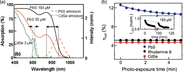
Figure 20. (a) Absorption and emission curves for CdSe/ZnS and PbS QDs with Stoke's shift indicated by double headed arrows, (b) optical efficiency of LSCs as a function of exposure time for PbS, CdSe, and Rhodamine B fluorophores, (inset) Reversal of photodarkening of PbS based LSC. Reprinted from [514], with the permission of AIP Publishing.
Download figure:
Standard image High-resolution imageConcerns over the toxicity of the materials used in LSCs have led to the search for QDs that do not require any heavy metals [490, 491]. Therefore, devices with CuInS2, AgInS2, and CuInSeS were developed with promising results [521–524]. In particular, CuInSexS2−x QDs in poly(lauryl methacrylate) have produced a colorless LSC, and the low reabsorption and high emission of the QDs allowed for optical power efficiency of 3.2% in a 12 × 12 × 0.3 cm3 large area LSC, making the possibility of LSC windows more realistic [524]. Moreover, Si QDs embedded in a polymerized acrylic matrix of area 144 cm2 have achieved PCE of 2.85%, while maintaining a transmittance of 70% [525]. Simulations showed that efficiency could exceed 5%, whereas flexible LSCs were fabricated, and along with simulation results, it was observed that the curvature of the device does not affect the performance. These results strongly encourage the potential implementation of LSCs in BIPV platforms.
4.3. Thin film based LSCs
While dyes and QDs are often implemented along with transparent polymer thin films in devices, work on opaque thin film based LSCs has not been as extensive due to the likelihood of increased self-absorption of the emitted light by the thin film itself, as well as the motivation for transparent LSCs as windows. Nevertheless, although opaque thin films might not be suitable for use as windows, they offer the potential of use in structures that require shading, such as bus stops [490].
QD-based LSCs suffer from limited quantum yield of the fluorophore, whereas dye-based LSCs suffer from photostability issues, hence alternative materials with more suitable properties are sought after. Hybrid organic–inorganic perovskites (PVSK) are in the forefront of photovoltaic research due to their excellent properties and have been used to fabricate high efficiency solar cells [526]. PVSKs can be prepared easily, using solution processing [527], and are characterized by broad absorption spectra, high quantum yield reaching 80% for thin films [527, 528], and refractive index of 2.5 that surpasses that of glass and polymer films [529, 530], both of which are necessary characteristics for a good LSC material. Recent work on PVSK-based LSCs, as shown in figure 21(a), has shown that despite the increased self-absorption shown by thin film LSCs, the use of materials with very high photoluminescence quantum yields and high absorption could make up for the self-absorption losses exhibited [531]. The devices reached optical efficiency of 29%, and were operational after seven weeks of storage in ambient conditions, as demonstrated in figure 21(b), demonstrating that while electrical properties of PVSK degrade quickly, the optical properties of PVSK are far more stable and can be leveraged for optical devices. This reveals that development of possible thin film materials with favorable optical properties can yield high efficiency thin film-based LSCs, a device architecture that has not been thoroughly explored in the past.

Figure 21. (a) Schematic of PVSK thin film LSC with Silicon PV attached at the end, (b) Optical efficiency of PVSK thin film LSCs: black dots represent initial optical efficiency, red crosses show the optical efficiency after 4 weeks of storage in ambient conditions. [531] John Wiley & Sons. Copyright © 2016, John Wiley and Sons.
Download figure:
Standard image High-resolution image
5. Conclusions and future outlook
The foray into nanostructured photovoltaics has been driven by the dual need for less expensive and more efficient PV devices. The encouraging trends and substantial progress summarized in the previous sections, combined with the wide variety of nanomaterials that are suited to serve as the active media, in combination with the many different designs and additives possible, has enlarged the scope of this field, making it all the more probable that a solution may be found. A summary of this field will, however, remain inadequate without some discussion of the shortcomings and concerns that are common to these materials.
The first and most obvious drawback is the fact that the device efficiencies remain, on average, lower than the traditional first and second-generation PVs. This is the reason that nanostructured PVs remain an 'emergent' technology, not yet ready to be integrated in to the grid in the form of modules. One of the causes that contribute to this is the inherent high surface-to-volume ratio of nanomaterials. This exacerbates the contribution of surface defects and trap states, which increase recombination losses and hinder the transport of photogenerated charge carriers. Mitigation of this particular issue requires increased focus on suitable architecture of nanostructures, such as one-dimensional materials, and surface ligands that allow improved charge conduction. Another fundamental problem that may also be addressed through suitable surface functionalization and modification of nanostructures is the matter of stability. Again, owing to the susceptibility of surface states, ambient environmental factors such as exposure to light and humidity can cause degradation of optical and electronic properties of nanomaterials. Dyes tend to photo bleach while semiconducting nanostructures are prone to photo-oxidation and darkening. The option of encapsulating and hermetically sealing the entire device is not an attractive one, as that adds to material costs.
On the topic of expenses, it is worth mentioning that to be truly cost-effective and achieve grid parity, the fabrication processes currently used for nano-synthesis will need to be scaled up for large scale production, allowing for roll-to-roll processing on industrial levels. Additionally, most of the nanomaterials used in PVs currently use heavy metals and other components that would not stand up to safe long-term use. Incorporating non-toxic elements, especially in the semiconducting nanomaterials will be imperative for future use.